Full-medium flat field scanning super-resolution planar lens
Technical Field
The invention belongs to the fields of micro-nano optics, optical focusing, diffractive optics and the like, and particularly relates to an all-dielectric flat-field scanning super-resolution planar lens.
Background
Conventional optical systems have a theoretical limit of 0.5 λ/NA (where λ is the wavelength and NA is the numerical aperture of the optical system). The super-resolution focusing has wide application prospect in the optical application fields of super-resolution imaging, particle control and the like. The super-surface structure can regulate and control the amplitude, phase and polarization of light, can be applied to the fields of optical focusing, beam shaping, holography and the like, and the lens based on the optical super-surface structure has the advantages of high transmittance, multiple functions (polarization conversion and beam focusing), light weight, easiness in integration and the like.
The current realization of far-field super-resolution focusing mainly comprises the following technical means.
For example, to generate a super-resolution solid focal spot, there are mainly: the documents related to the binary amplitude super-oscillation lens, the binary phase super-oscillation lens and the continuous amplitude phase super-oscillation lens, wherein the focusing light spots of the lenses are all smaller than the diffraction limit (0.5 lambda/NA), include:
·E.T.Rogers,S.Savo,J.Lindberg,T.Roy,M.R.Dennis,N.I.Zheludev,“Superoscillatory optical needle”.Appl.Phys.Lett.,Vol.102,031108(2013).
·K.Huang,H.Ye,J.Teng,S.P.Yeo,B.Lukyanchuk,C.Qiu,“Optimization-free superoscillatory lens using phase and amplitude masks”.Laser Photonics Rev.Vol.8,pp152-157(2014).
·G.Yuan,E.T.F.Rogers,T.Roy,G.Adamo,Z.Shen,N.I.Zheludev,“Planar superoscillatory lens for sub-diffraction optical needles at violet wavelengths”.Sci.Rep.Vol.4,pp6333-6333(2015).
·Yu Anping,Chen Gang,Zhang Zhihai,Wen Zhongquan,Dai Luru,Zhang Kun,Jiang Senlin,Wu Zhixiang,Yuyan Li,Changtao Wang and Xiangang Luo,“Creation of Sub-diffraction Longitudinally Polarized Spot by Focusing Radially Polarized Light with Binary Phase Lens”,Scientific Reports,Vol.6,pp38859(2016)
·R.Zuo,W.Liu,H.Cheng,S.Chen,J.Tian,“Breaking the Diffraction Limit with Radially Polarized Light Based on Dielectric Metalenses”.Adv.Opt.Mater.Vol.6,pp1800795(2018).
·G.Yuan,K.Rogers,E.T.F.Rogers,N.I.Zheludev,“Far-Field Superoscillatory Metamaterial Superlens”,Phys.Rev.Appl.,Vol.11,pp064016(2019).
for example, to generate super-resolution hollow focal spots, there are mainly: focusing the angular polarized light by adopting a traditional objective lens and a cone lens to obtain a hollow focal spot focusing light spot; double-ring angular polarized light is used as incident light, and a traditional objective lens is combined to form a hollow focal spot; aiming at incident light with different polarization states and topological charges, focusing by adopting a high numerical aperture lens optimized by a pupil function (amplitude and phase), and generating super-resolution focusing through numerical calculation; the conversion from linearly polarized light to linearly symmetric vector polarized light is realized by adopting a polarization converter (S glass sheet), and the linearly polarized light is used as incident light and is focused by a binary phase type plane super-oscillation lens to form super-resolution focusing. The relevant documents are:
·Tian Bo and Pu Jixiong.“Tight focusing ofa double-ring-shaped,azimuthally polarized beam”.Opt.Let.Vol.36,pp 2014-2016(2011).
·Lalithambigai K,Suresh P,Ravi V,Prabakaran K,Jaroszewicz Z,Rajesh K.B.,Anbarasan P.M.and Pillai T.V.S.“Generation of sub wavelength super-long dark channel using highNA lens axicon”.Opt.Let.Vol.37,pp 999-1001(2012).
·Chen Gang,Wu Zhixiang,Yu Anping,Zhihai Zhang,Zhongquan Wen,Kun Zhang,Luru Dai,Senlin Jiang,Yuyan Li,Li Chen,Changtao Wang and Xiangang Luo.“Generation ofa sub-diffraction hollow ring by shaping an azimuthally polarized wave”.Scientific Reports,Vol.6,pp37776-37785(2016).
·Zhixiang Wu,Qijian Jin,Shuo Zhang,Kun Zhang,Lingfang Wang,Luru Dai,Zhongquan Wen,Zhihai Zhang,Gaofeng Liang,Yufei Liu,Gang Chen,Generating a three-dimensional hollow spot with sub-diffraction transverse size by a focused cylindrical vector wave,Optics Express,Vol.26,pp.7866-7875(2018)
·Zhixiang Wu,Fengliang Dong,Shuo Zhang,Saokui Yan,Gaofeng Liang,Zhihai Zhang,Zhongquan Wen,Gang Chen,Luru Dai,Weiguo Chu,Broadband dielectric metalens for polarization manipulating and superoscillation focusing of visible light,ACS Photonics,Vol.7,pp180-189(2019).
however, the above method can only achieve super-resolution focusing on a vertical incident beam, and cannot achieve super-resolution focusing on an oblique incident beam.
Because the existing super-resolution lens can only realize super-resolution focusing on a vertical incident beam and cannot realize super-resolution focusing on an oblique incident beam, the existing non-labeled far-field super-resolution microscope system based on the super-resolution lens can only adopt sample moving scanning, the scanning speed is low, and the application of the existing non-labeled far-field super-resolution microscope system based on the super-resolution lens is greatly restricted. The relevant documents are:
·E.T.F.Rogers,et al.A super-oscillatory lens optical microscope for subwavelength imaging.Nat.Mater.,Vol.11,pp432–435(2012).
·F.Qin,et al.A supercritical lens optical label-free microscopy:sub-diffraction resolution andultra-long working distance.Adv.Mater.29,1602721(2017).
disclosure of Invention
Aiming at the defects of the prior art, the invention provides an all-dielectric flat-field scanning super-resolution planar lens, which is a flat-field scanning super-resolution planar lens based on an all-dielectric geometric phase super-surface unit, realizes the super-resolution focusing function and the flat-field scanning function simultaneously, and has the functions of broadband super-resolution focusing and flat-field scanning.
The invention provides a full-medium flat-field scanning super-resolution planar lens, which adopts circularly polarized collimated light beams as incident light beams, wherein the incident light beams are incident to a cuboid medium structure from one side of a substrate and are in a wavelength range [ lambda ]1,λ2]Within, for any given operating wavelength λ (λ)1≤λ≤λ2) The circularly polarized collimated incident light can be made to have a range of incident angles [ -theta [ - ]Max,+θMax]The focal length f (lambda) of the solid focal spot is related to the working wavelength lambda; the transverse focal spot size (full width at half maximum) is less than the diffraction limit 0.5 λ/NA, where NA is sin (β) and tan (β) is Rlens/f(λ),RlensF (lambda) is the effective use radius of the full-medium flat field scanning super-resolution plane lens and the focal length corresponding to the working wavelength lambda; for collimated circularly polarized incident light with an incident angle of theta (-theta)Max≤θ≤+θMax) The offset d of the center of the corresponding orthogonal circularly polarized focusing spot in the focal plane is linear with the incident angle theta, that is, d (theta) is C × theta × f (lambda), where C is a real constant.
The invention is realized by the following technical scheme:
the lens consists of all-dielectric geometric phase super-surface units distributed in a periodic array, the period of all-dielectric geometric phase super-surface units is T, the lens comprises a cuboid dielectric structure and a substrate of a corresponding part below the cuboid dielectric structure, and the centers of each cuboid dielectric structure and the all-dielectric geometric phase super-surface units of the cuboid dielectric structure are superposed in an XY plane.
The substrate is of thickness tsubRefractive index of nsubIn the operating wavelength range [ lambda ]1,λ2]A transparent dielectric material S with low absorptivity (absorption coefficient less than 0.01) and parallel upper and lower surfaces.
The side lengths of the cuboid medium structure are L and W respectively, and the height is H. The refractive index of the cuboid dielectric structure is ndIn the operating wavelength range [ lambda ]1,λ2]Has low absorptivity (absorption coefficient less than 0.01).
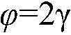
The phase of the orthogonal circularly polarized light (orthogonal to the polarization direction of the incident circularly polarized light) emitted by the all-dielectric geometric phase super-surface unit under the incident condition of circularly polarized light
Can be changed by setting the direction angle gamma of the cuboid dielectric structure (namely the included angle between the side length L of the cuboid dielectric structure and the positive direction of the X axis), and the corresponding phase is
The value range of gamma is more than or equal to 0 and less than or equal to gamma<Pi, the phase range of the emitted orthogonal circularly polarized light is
Therefore, continuous phase regulation and control of emergent orthogonal circularly polarized light can be realized by setting the direction angle of the cuboid medium structure.
Effective use radius R of the lenslensN × T, where N is the maximum number of all-dielectric geometric phase super-surface units along the radius direction, and T is the period of all-dielectric geometric phase super-surface units. The lens is divided into N in a periodic array of cells2(N columns and N rows) of all-dielectric geometric phase super-surface elements, the phase distribution of the lens in the radial direction satisfying psi (r), wherein 0 ≦ psi (r)<2 pi. In the ith row,The phase in the all-dielectric geometric phase super-surface cell of the j-th column is psi (r)ij) The direction angle of the corresponding cuboid dielectric structure satisfies gammaij=ψ(rij) A first reaction system of a first reaction system and a second reaction system of a second reaction systemijAnd the distances from the central positions of the all-dielectric geometric phase super-surface units in the ith row and the jth column to the central position of the all-dielectric flat-field scanning super-resolution plane lens are represented.
The full-medium flat-field scanning super-resolution planar lens provided by the invention has a central working wavelength lambdac=λ1+λ2The circularly polarized collimated incident light can be made to have a range of incident angles [ -theta [ - ]Max,+θMax]Converging the solid focal spots into orthogonal circular polarization (orthogonal to the polarization direction of incident circular polarized light) on the same focal plane; transverse focal spot size (full width at half maximum) less than diffraction limit 0.5 lambdaca/NA, where NA is sin (β) and tan (β) Rlens/fc,RlensAnd fcRespectively, effective use radius of the lens and central operating wavelength lambdacThe corresponding focal length.
The full-medium flat-field scanning super-resolution planar lens can be used in a wavelength range [ lambda ]1,λ2]Within, for any given operating wavelength λ (λ)1≤λ≤λ2) The circularly polarized collimated incident light can be made to have a range of incident angles [ -theta [ - ]Max,+θMax]The focal length f (lambda) of the solid focal spot is related to the working wavelength lambda; the transverse focal spot size (full width at half maximum) is less than the diffraction limit 0.5 λ/NA, where NA is sin (β) and tan (β) is Rlens/f(λ),RlensAnd f (λ) are the effective use radius of the face lens and the focal length corresponding to the operating wavelength λ, respectively.
The full-medium flat-field scanning super-resolution planar lens provided by the invention can collimate circularly polarized incident light (-theta) with an incident angle thetaMax≤θ≤+θMax) The offset d of the center of the corresponding orthogonal circularly polarized focusing spot in the focal plane is linear with the incident angle theta, that is, d (theta) is C × theta × f (lambda), where C is a real constant.
For the present hairThe full-medium flat-field scanning super-resolution planar lens has a circular effective area and a central wavelength of lambdac=λ1+λ2Effective use radius of RlensFocal length of fc(ii) a For a central wavelength λcAccording to given target parameters (such as maximum full width at half maximum, peak intensity, side lobe ratio, scanning angle, focal spot offset and the like) of the focal spot on the focal plane, an optimization algorithm is adopted: namely a design scheme combining a light field diffraction calculation method (such as a vector angular spectrum diffraction method, Rayleigh-Sophia vector diffraction integral, Debye-Volvov vector diffraction integral and the like) and a multi-target-multi-parameter optimization algorithm (such as a particle swarm optimization algorithm, a simulated annealing algorithm, a particle swarm optimization algorithm, a genetic algorithm, an ant colony optimization algorithm, a black hole number algorithm and the like), and the phase distribution psi (r) of the full-medium flat field scanning super-resolution planar lensij)(0≤ψ(rij)<Pi) are optimally designed (wherein r isijDistance from the center position of the all-dielectric geometric phase super-surface unit in the ith row and the jth column to the center position of the all-dielectric flat-field scanning super-resolution plane lens) to make the center position of the all-dielectric geometric phase super-surface unit have the central working wavelength lambdac=λ1+λ2The circularly polarized collimated incident light can be made to have a range of incident angles [ -theta [ - ]Max,+θMax]Converging the solid focal spots into orthogonal circular polarization (orthogonal to the polarization direction of incident circular polarized light) on the same focal plane; transverse focal spot size (full width at half maximum) less than diffraction limit 0.5 lambdaca/NA, where NA is sin (β) and tan (β) Rlens/fc,RlensAnd fcEffective use radius and central working wavelength lambda of all-dielectric flat field scanning super-resolution planar lenscThe corresponding focal length.
For the all-dielectric flat-field scanning super-resolution planar lens, the all-dielectric geometric phase super-surface unit can be in the wavelength range [ lambda ] due to the broadband characteristic and the dispersion characteristic of the all-dielectric geometric phase super-surface unit1,λ2]Within, for any given operating wavelength λ (λ)1≤λ≤λ2) The circularly polarized collimated incident light can be made to have a range of incident angles [ -theta [ - ]Max,+θMax]In the same focal planeConverging into an orthogonal circularly polarized (orthogonal to the polarization direction of the incident circularly polarized light) solid focal spot, the focal length f (λ) of which is related to the operating wavelength λ; the transverse focal spot size (full width at half maximum) is less than the diffraction limit 0.5 λ/NA, where NA is sin (β) and tan (β) is Rlens/f(λ),RlensF (lambda) is the effective use radius of the full-medium flat field scanning super-resolution plane lens and the focal length corresponding to the working wavelength lambda; for collimated circularly polarized incident light with an incident angle of theta (-theta)Max≤θ≤+θMax) The offset d of the center of the corresponding orthogonal circularly polarized focusing spot in the focal plane is linear with the incident angle theta, that is, d (theta) is C × theta × f (lambda), where C is a real constant.
In summary, the all-dielectric flat-field scanning super-resolution planar lens provided by the invention realizes the phase of emergent orthogonal circularly polarized light by setting the direction angle gamma of the cuboid dielectric structure of the all-dielectric geometric phase super-surface unit for circularly polarized incident light
Continuous regulation in the [0, 2 π) range; the phase space distribution psi (r) required by the full-medium flat-field scanning super-resolution planar lens is optimally designed, the required direction angle of the full-medium geometric phase super-surface unit cuboid medium structure at the corresponding position is calculated according to the relation between the phase and the direction angle gamma of the full-medium geometric phase super-surface unit cuboid medium structure, the full-medium geometric phase super-surface unit arrangement of the whole full-medium flat-field scanning super-resolution planar lens is completed, and the phase space distribution required by the whole lens is realized; circularly polarized light with the wavelength of lambda is used as incident light beam to enter the cuboid medium structure from the substrate side, and the incident light beam is within the range of-theta
Max,+θ
Max]And a focused spot smaller than the optical diffraction limit (0.5 lambda/NA) is generated at a position distant from the exit surface of the lens by a focal length f (lambda). For collimated circularly polarized incident light with an incident angle of theta (-theta)
Max≤θ≤+θ
Max) The offset d of the center of the corresponding orthogonal circularly polarized focusing spot in the focal plane is linear with the incident angle theta, that is, d (theta) is C × theta × f (lambda), where C is a real constant.
The full-medium flat-field scanning super-resolution planar lens provided by the invention has the advantages of high transmittance, integration of super-resolution focusing and ordinary scanning functions, light weight, easiness in integration and the like, and can be applied to the fields of optical focusing, optical imaging, super-resolution optical microscopy and the like.
Drawings
FIG. 1a, FIG. 1b, FIG. 1c, FIG. 1d are schematic structural and functional diagrams of all-dielectric geometric phase super-surface unit composing an all-dielectric flat-field scanning super-resolution planar lens;
FIG. 2 shows the direction angle γ of the cuboid dielectric structure of the all-dielectric geometric phase super-surface unit and the phase of the corresponding orthogonal circularly polarized emergent light under the condition of circularly polarized incident light
A relationship diagram of (1);
FIG. 3a is a schematic structural diagram of an all-dielectric flat-field scanning super-resolution planar lens; FIG. 3b is an enlarged view of the central portion of FIG. 3 a;
FIG. 4 is a phase space distribution diagram of an all-dielectric flat-field scanning super-resolution planar lens;
FIG. 5 is a schematic focusing diagram of a flat-field scanning super-resolution planar lens;
FIG. 6 is a diagram showing the intensity distribution of the light field in the X-axis direction and the Y-axis direction through the center of the focal spot in the focal plane of the full-dielectric flat-field scanning super-resolution planar lens for different incident angles under the condition of circularly polarized incident light with a wavelength of 632.8 nm;
FIG. 7 is a diagram showing the relationship between focal spot parameters and incident angle in the focal plane of an all-dielectric flat-field scanning super-resolution planar lens under a circularly polarized incident light with a wavelength of 632.8 nm;
FIG. 8 is a diagram showing the relationship between the focal spot center position and the incident angle in the focal plane of the full-dielectric flat-field scanning super-resolution planar lens under the condition of circularly polarized incident light with a wavelength of 632.8 nm;
FIG. 9 is a diagram showing the intensity distribution of the light field in the X-axis direction and the Y-axis direction through the center of the focal spot in the focal plane of the full-dielectric flat-field scanning super-resolution planar lens for different incident angles under the condition of circularly polarized incident light with a wavelength of 620.0 nm;
FIG. 10 is a graph showing the relationship between the focal spot parameters and the incident angle in the focal plane of the full-dielectric flat-field scanning super-resolution planar lens under the condition of circularly polarized incident light with a wavelength of 620.0 nm;
FIG. 11 is a diagram showing the intensity distribution of the light field in the X-axis direction and the Y-axis direction through the center of the focal spot in the focal plane of the full-dielectric flat-field scanning super-resolution planar lens for different incident angles under the condition of circularly polarized incident light with a wavelength of 630.0 nm;
FIG. 12 is a diagram showing the relationship between the focal spot parameters and the incident angle in the focal plane of the full-dielectric flat-field scanning super-resolution planar lens under the condition of circularly polarized incident light with the wavelength of 630.0 nm;
FIG. 13 is a diagram showing the intensity distribution of the light field in the X-axis direction and the Y-axis direction through the center of the focal spot in the focal plane of the full-dielectric flat-field scanning super-resolution planar lens for different incident angles under the condition of circularly polarized incident light with a wavelength of 640.0 nm;
FIG. 14 is a diagram of the relationship between the focal spot parameters and the incident angle in the focal plane of the full-medium flat-field scanning super-resolution planar lens under the condition of circularly polarized incident light with the wavelength of 640.0 nm;
FIG. 15 is a diagram showing the distribution of the intensity of the light field in the X-axis direction and the Y-axis direction through the center of the focal spot in the focal plane of the full-dielectric flat-field scanning super-resolution planar lens for different incident angles under the condition of circularly polarized incident light with a wavelength of 650.0 nm;
FIG. 16 is a graph showing the relationship between the focal spot parameters and the incident angle in the focal plane of the full-dielectric flat-field scanning super-resolution planar lens under the condition of circularly polarized incident light with a wavelength of 650.0 nm;
FIG. 17 is a diagram showing the intensity distribution of the light field in the X-axis direction and the Y-axis direction through the center of the focal spot in the focal plane of the full-dielectric flat-field scanning super-resolution planar lens for different incident angles under the condition of circularly polarized incident light with a wavelength of 660.0 nm;
FIG. 18 is a diagram of the relationship between the focal spot parameters and the incident angle in the focal plane of the full-medium flat-field scanning super-resolution planar lens under the condition of circularly polarized incident light with the wavelength of 660.0 nm;
FIG. 19 shows focal plane positions at wavelengths λ of 620.0nm, 630.0nm, 640.0nm, 650.0nm, 660.0nm, respectively
Detailed Description
The technical solution of the present invention is further described below with reference to the accompanying drawings.
Fig. 1a, fig. 1b and fig. 1c show the structure schematic diagram of an all-dielectric geometric phase super-surface unit composed of a
substrate 1 and a cuboid
dielectric block 2, which forms an all-dielectric flat-field scanning super-resolution planar lens. In the structure, the center of a cuboid dielectric block coincides with the center of a unit structure, the period of a full-dielectric geometric phase super-surface unit is T, the height of the full-dielectric geometric phase super-surface unit is H, the length of the full-dielectric geometric phase super-surface unit is L, and the width of the full-dielectric geometric phase super-surface unit is W. FIG. 1d shows the phase of the emergent light corresponding to orthogonal circular polarization when the direction angle of the cuboid dielectric structure of the all-dielectric geometric phase super-surface unit is γ (the angle between the length direction and the X-axis positive direction) under the condition of circularly polarized incident light
The situation (2).
The substrate 1 is of thickness tsubRefractive index of nsubIn the operating wavelength range [ lambda ]1,λ2]A transparent dielectric material S with low absorptivity (absorption coefficient less than 0.01) and parallel upper and lower surfaces.
The material and structure parameters of the full-medium flat field scanning super-resolution planar lens are designed as follows:
1. selection of substrate materials
For a range of operating wavelengths lambda1,λ2]A medium material of a transparent material with low absorptivity (absorption coefficient less than 0.01) is selected as a focusing lens substrate. For example: for the operating wavelength range [520nm-690nm]Sapphire glass, quartz glass, etc. can be selected.
2. Selection of cuboid dielectric structure material
For a range of operating wavelengths lambda1,λ2]The dielectric material with low absorptivity (absorption coefficient less than 0.01) and high refractive index (refractive index greater than 1.5) is selected as the cuboid dielectric structure material of the all-dielectric geometric phase super-surface unit, and the dielectric material with higher refractive index can meet the phase requirement and ensure smaller all-dielectric materialThe geometric phase exceeds the surface element thickness. For example: for the operating wavelength range [450nm-690nm]Optionally Amorphous silicon (Amorphous silicon), titanium dioxide (TiO)2) And gallium phosphide (GaP) as the material of the all-dielectric geometric phase super-surface unit.
3. Structural dimensioning of cuboid dielectric structures
According to the central operating wavelength lambda
c=λ
1+λ
2And a medium material D, wherein in order to realize the phase regulation function of the all-medium geometric phase super-surface unit, finite element simulation software FDTD is adopted to scan and optimize the period T, the height H, the length L and the width W of the unit structure, and under the condition that incident light is circularly polarized light, the phase of the emergent light of orthogonal circular polarization is continuously adjustable on the premise that the all-medium geometric phase super-surface unit has higher amplitude transmittance. For example, for a center wavelength λ of 632.8nm, the structure size of all-dielectric geometric phase super-surface units using Amorphous silicon (Amorphous silicon) is optimized to be T300 nm, H320 nm, L200 nm, and W116 nm. FIG. 2 shows the direction angle gamma of the cuboid dielectric structure of the all-dielectric geometric phase super-surface unit and the phase of the corresponding orthogonal circularly polarized emergent light under the condition of circularly polarized incident light

A graph of the relationship (c). Phase of emergent light
The direction angle gamma with the cuboid dielectric structure satisfies
And the amplitude transmittances were all greater than 0.72 (the amplitude transmittance could be further improved by increasing the height H of the rectangular parallelepiped structure).
4. Unit array arrangement of all-dielectric geometric phase super-surface unit in all-dielectric flat field scanning super-resolution planar lens
Effective use radius R of all-dielectric flat-field scanning super-resolution planar lenslensN x T, where N is the full-dielectric geometric phase super-surface along the radius directionThe maximum number of the units, and T is the period of the all-dielectric geometric phase super-surface unit. As shown in FIGS. 3a and 3b, the all-dielectric flat-field scanning super-resolution planar lens is divided into N in a periodic array of cells2(N columns and N rows) of all-dielectric geometric phase super-surface units, rijAnd the distances from the central positions of the all-dielectric geometric phase super-surface units in the ith row and the jth column to the central position of the all-dielectric flat-field scanning super-resolution plane lens are represented. The phase distribution of the all-dielectric flat-field scanning super-resolution planar lens along the radial direction meets psi (r), wherein psi (r) is more than or equal to 0<2 pi. The phase in the all-dielectric geometric phase super-surface unit in the ith row and the jth column is psi (r)ij) The direction angle of the corresponding cuboid dielectric structure satisfies gammaij=ψ(rij)/2。
5. Phase distribution optimization of full-medium flat field scanning super-resolution planar lens
For a central operating wavelength lambdacSetting the structural parameters and focusing spot parameters of the full-medium flat-field scanning super-resolution planar lens, including the effective use radius R of the full-medium flat-field scanning super-resolution planar lenslensFocal length fcAll-dielectric geometric phase super-surface unit period T and incidence angle range [ -theta [ ]Max,+θMax]And the transverse full width at half maximum (FWHM) of the focused spot at the focal plane<0.5λc/NA), side lobe ratio (SR, ratio of maximum side lobe intensity to peak intensity), and peak intensity, etc. For a central wavelength of λcThe method adopts a vector angle spectrum theory diffraction calculation formula combined with a particle swarm optimization algorithm (the calculation method is shown in E.T.F. Rogers, J.Lindberg, T.Roy, S.Savo, J.E.Chad, M.R.Dennis, and N.I.ZHELudev, A super-optics lens optical microscope sub-wavelength imaging, Nat.Mater.Vol.11, pp.432-435(2012)), and scans the phase distribution psi of the super-resolution planar lens (r.F.Rogers, J.Lindberg, T.Roy, S.Savo, J.E.Chad.M.R.Dennis) on the whole medium flat fieldij) Optimized design is carried out, the circularly polarized collimated light beam is used as an incident light beam, the incident light beam enters the cuboid medium structure from one side of the substrate, and the incident light beam is within a given incident angle range of-theta on a set focal planeMax≤θ≤+θMaxIn practice, for M angles θ i (i ═ 1, …, M, considerTaking the symmetry into consideration, take theta0=0,…,θM=θMax. And ensures that the relative offset of the corresponding focus of two adjacent angles in the focal plane is less than 0.1 lambdac) So that the focused spot has a full width at half maximum (FWHM)<0.5λcThe power amplifier meets the set requirements of/NA), side lobe ratio (SR, the ratio of the maximum side lobe intensity to the peak intensity) and peak intensity, and the offset d of the focal spot on the focal plane is in a linear relation with the incident angle theta, namely d (theta) is equal to C multiplied by theta multiplied by fcWhere C is a real constant (typically C ═ 1). Transverse focal spot size (full width at half maximum) less than diffraction limit 0.5 lambdaca/NA, where NA is sin (β) and tan (β) Rlens/fc,RlensAnd fcEffective use radius and working wavelength lambda of all-dielectric flat field scanning super-resolution planar lenscThe corresponding focal length.
FIG. 4 shows λc=632.8nm,Rlens=240λcFocal length fc=60λcAnd optimizing the design result by the phase.
FIG. 5 shows a focusing diagram of an all-dielectric flat-field scanning super-resolution planar lens at a given incident angle range-thetaMax≤θ≤+θMaxFor a wavelength λ (λ)1≤λ≤λ2) Can be focused on a focal plane at a distance f from the emission end, and the full width at half maximum of the focal spot is less than the diffraction limit of 0.5 lambda/NA, wherein NA is sin (atan (R)lens/f)); meanwhile, the offset d of the focal spot on the focal plane is proportional to the incident angle θ, i.e., d (θ) ═ C × θ × f, where C is a real constant (usually, C ═ 1).
FIG. 6 shows the wavelength λ ═ λcUnder the condition of circularly polarized incident light of (632.8nm), the light field intensity distribution diagram is formed in the focal plane of the full-medium flat-field scanning super-resolution planar lens along the X-axis direction and the Y-axis direction through the center of the focal spot for different incident angles (namely 0 degrees, 0.25 degrees, 0.5 degrees, 0.75 degrees, 1.0 degrees, 1.25 degrees, 1.5 degrees, 1.75 degrees and 2.0 degrees).
Fig. 7 shows the wavelength λ ═ λcUnder the condition of circularly polarized incident light of (632.8nm), focal spots in focal planes of all-dielectric flat-field scanning super-resolution planar lensesA plot of parameters versus angle of incidence, including the transverse full width at half maximum (FWHM) of the focused spot at the focal planexAnd FWHMyFull width at half maximum of the focal spot in the X-direction and Y-direction, respectively), side lobe ratio (SR, ratio of maximum side lobe intensity to peak intensity, SRxAnd SRySide lobe ratios in the X and Y directions, respectively) and peak intensity as a function of angle of incidence, with the dashed line giving the corresponding optical diffraction limit (0.5 λ/NA). The maximum transverse full width at half maximum (FWHM) of the focused spot is less than the diffraction limit over all ranges of incident angles.
Fig. 8 shows the relationship between the offset d of the focal spot center position in the focal plane and the incident angle theta.
5. Broadband working characteristic of full-medium flat field scanning super-resolution planar lens
In a given wavelength range [ lambda ]1,λ2]For a wavelength λ (λ)1≤λ≤λ2) The circularly polarized collimated light beam is used as an incident light beam, the incident light beam is incident to the cuboid medium structure from one side of the substrate, and is in a given incident angle range of-theta on a set focal planeMax≤θ≤+θMaxAnd (3) calculating by using a vector angle spectrum diffraction theory to obtain: the optical field intensity distribution of the focal spot center along the X-axis direction and the Y-axis direction on the focal plane, the transverse full width at half maximum (FWHM) of the focal spot, the side lobe ratio (SR, the ratio of the maximum side lobe intensity to the peak intensity), the peak intensity, and the like, and the relationship between the offset d of the focal spot center position in the focal plane and the incident angle θ.
Fig. 9 is a diagram showing a distribution of optical field intensity along the X-axis direction and the Y-axis direction through the focal spot center in the focal plane of the all-dielectric flat-field scanning super-resolution planar lens for different incident angles (i.e., 0 °, 0.25 °, 0.5 °, 0.75 °, 1.0 °, 1.25 °, 1.5 °, 1.75 °, and 2.0 °) in the case of circularly polarized incident light with a wavelength λ of 620.0 nm.
FIG. 10 is a graph of focal spot parameters in the focal plane of an all-dielectric flat-field scanning super-resolution planar lens as a function of incident angle for circularly polarized incident light with a wavelength λ of 620.0nm, including the transverse full width at half maximum (FWHM ) of the focused spot on the focal planexAnd FWHMyFull width at half maximum of the focal spot in the X-direction and Y-direction, respectively), side lobe ratio (SR, ratio of maximum side lobe intensity to peak intensity, SRxAnd SRySide lobe ratios in the X and Y directions, respectively) and peak intensity as a function of angle of incidence, with the dashed line giving the corresponding optical diffraction limit (0.5 λ/NA). The maximum transverse full width at half maximum (FWHM) of the focused spot is less than the diffraction limit over all ranges of incident angles.
Fig. 11 is a graph showing the intensity distribution of the optical field along the X-axis direction and the Y-axis direction through the center of the focal spot in the focal plane of the all-dielectric flat-field scanning super-resolution planar lens for different incident angles (i.e., 0 °, 0.25 °, 0.5 °, 0.75 °, 1.0 °, 1.25 °, 1.5 °, 1.75 °, and 2.0 °) in the case of circularly polarized incident light with a wavelength λ of 630.0 nm.
FIG. 12 is a diagram of focal spot parameters in the focal plane of an all-dielectric flat-field scanning super-resolution planar lens as a function of incident angle under circularly polarized incident light with a wavelength λ of 630.0nm, including the transverse full width at half maximum (FWHM ) of the focused spot on the focal planexAnd FWHMyFull width at half maximum of the focal spot in the X-direction and Y-direction, respectively), side lobe ratio (SR, ratio of maximum side lobe intensity to peak intensity, SRxAnd SRySide lobe ratios in the X and Y directions, respectively) and peak intensity as a function of angle of incidence, with the dashed line giving the corresponding optical diffraction limit (0.5 λ/NA). The maximum transverse full width at half maximum (FWHM) of the focused spot is less than the diffraction limit over all ranges of incident angles.
Fig. 13 is a graph showing the intensity distribution of the optical field along the X-axis direction and the Y-axis direction through the center of the focal spot in the focal plane of the all-dielectric flat-field scanning super-resolution planar lens for different incident angles (i.e., 0 °, 0.25 °, 0.5 °, 0.75 °, 1.0 °, 1.25 °, 1.5 °, 1.75 °, and 2.0 °) in the case of circularly polarized incident light with a wavelength λ of 640.0 nm.
FIG. 14 is a graph of focal spot parameters in the focal plane of an all-dielectric flat-field scanning super-resolution planar lens versus incident angle for circularly polarized incident light with wavelength λ of 640.0nm, including the transverse full width at half maximum (FWHM ) of the focused spot at the focal planexAnd FWHMyFull width at half maximum of the focal spot in the X-direction and Y-direction, respectively), side lobe ratio (SR, ratio of maximum side lobe intensity to peak intensity, SRxAnd SRySide lobe ratios in the X and Y directions, respectively) and peak intensity as a function of angle of incidence, with the dashed line giving the corresponding optical diffraction limit (0.5 λ/NA). The maximum transverse full width at half maximum (FWHM) of the focused spot is less than the diffraction limit over all ranges of incident angles.
Fig. 15 is a diagram showing a distribution of optical field intensity along the X-axis direction and the Y-axis direction through the focal spot center in the focal plane of the all-dielectric flat-field scanning super-resolution planar lens for different incident angles (i.e., 0 °, 0.25 °, 0.5 °, 0.75 °, 1.0 °, 1.25 °, 1.5 °, 1.75 °, and 2.0 °) in the case of circularly polarized incident light having a wavelength λ of 650.0 nm.
FIG. 16 is a graph of focal spot parameters in the focal plane of an all-dielectric flat-field scanning super-resolution planar lens as a function of incident angle for circularly polarized incident light with a wavelength λ of 650.0nm, including the transverse full width at half maximum (FWHM ) of the focused spot on the focal planexAnd FWHMyFull width at half maximum of the focal spot in the X-direction and Y-direction, respectively), side lobe ratio (SR, ratio of maximum side lobe intensity to peak intensity, SRxAnd SRySide lobe ratios in the X and Y directions, respectively) and peak intensity as a function of angle of incidence, with the dashed line giving the corresponding optical diffraction limit (0.5 λ/NA). The maximum transverse full width at half maximum (FWHM) of the focused spot is less than the diffraction limit over all ranges of incident angles.
Fig. 17 is a graph showing the intensity distribution of the light field along the X-axis direction and the Y-axis direction through the center of the focal spot in the focal plane of the all-dielectric flat-field scanning super-resolution planar lens for different incident angles (i.e., 0 °, 0.25 °, 0.5 °, 0.75 °, 1.0 °, 1.25 °, 1.5 °, 1.75 °, and 2.0 °) in the case of circularly polarized incident light with a wavelength λ of 660.0 nm.
FIG. 18 is a graph of focal spot parameters in the focal plane of an all-dielectric flat-field scanning super-resolution planar lens versus incident angle for circularly polarized incident light with wavelength λ of 660.0nm, including the transverse full width at half maximum (FWHM ) of the focused spot at the focal planexAnd FWHMyAre respectively asFull width at half maximum of the focal spot in the X-direction and the Y-direction), side lobe ratio (SR, ratio of maximum side lobe intensity to peak intensity, SRxAnd SRySide lobe ratios in the X and Y directions, respectively) and peak intensity as a function of angle of incidence, with the dashed line giving the corresponding optical diffraction limit (0.5 λ/NA). The maximum transverse full width at half maximum (FWHM) of the focused spot is less than the diffraction limit over all ranges of incident angles.
FIG. 19 shows focal plane positions at wavelengths λ of 620.0nm, 630.0nm, 640.0nm, 650.0nm, 660.0nm, respectively.
The full-medium, broadband polarization and phase control super-surface and far-field super-resolution focusing full-medium flat-field scanning super-resolution planar lens provided by the invention is not only suitable for optical wave bands, but also can be expanded to other electromagnetic wave bands.
The applicant has described and illustrated embodiments of the present invention in detail with reference to the drawings attached hereto, but it should be understood by those skilled in the art that the above embodiments are only preferred embodiments of the present invention, and the detailed description is only for the purpose of helping the reader to better understand the spirit of the present invention, and is not meant to limit the scope of the present invention, but rather, any modifications based on the spirit of the present invention are made.


