CN110914992A - Infrared multispectral imaging device and method - Google Patents
Infrared multispectral imaging device and method Download PDFInfo
- Publication number
- CN110914992A CN110914992A CN201880037340.8A CN201880037340A CN110914992A CN 110914992 A CN110914992 A CN 110914992A CN 201880037340 A CN201880037340 A CN 201880037340A CN 110914992 A CN110914992 A CN 110914992A
- Authority
- CN
- China
- Prior art keywords
- elementary
- filter
- matrix array
- filters
- detection
- Prior art date
- Legal status (The legal status is an assumption and is not a legal conclusion. Google has not performed a legal analysis and makes no representation as to the accuracy of the status listed.)
- Granted
Links
Images


Classifications
-
- H—ELECTRICITY
- H10—SEMICONDUCTOR DEVICES; ELECTRIC SOLID-STATE DEVICES NOT OTHERWISE PROVIDED FOR
- H10F—INORGANIC SEMICONDUCTOR DEVICES SENSITIVE TO INFRARED RADIATION, LIGHT, ELECTROMAGNETIC RADIATION OF SHORTER WAVELENGTH OR CORPUSCULAR RADIATION
- H10F39/00—Integrated devices, or assemblies of multiple devices, comprising at least one element covered by group H10F30/00, e.g. radiation detectors comprising photodiode arrays
- H10F39/10—Integrated devices
- H10F39/12—Image sensors
- H10F39/18—Complementary metal-oxide-semiconductor [CMOS] image sensors; Photodiode array image sensors
- H10F39/184—Infrared image sensors
-
- G—PHYSICS
- G01—MEASURING; TESTING
- G01J—MEASUREMENT OF INTENSITY, VELOCITY, SPECTRAL CONTENT, POLARISATION, PHASE OR PULSE CHARACTERISTICS OF INFRARED, VISIBLE OR ULTRAVIOLET LIGHT; COLORIMETRY; RADIATION PYROMETRY
- G01J3/00—Spectrometry; Spectrophotometry; Monochromators; Measuring colours
- G01J3/12—Generating the spectrum; Monochromators
-
- G—PHYSICS
- G01—MEASURING; TESTING
- G01J—MEASUREMENT OF INTENSITY, VELOCITY, SPECTRAL CONTENT, POLARISATION, PHASE OR PULSE CHARACTERISTICS OF INFRARED, VISIBLE OR ULTRAVIOLET LIGHT; COLORIMETRY; RADIATION PYROMETRY
- G01J3/00—Spectrometry; Spectrophotometry; Monochromators; Measuring colours
- G01J3/28—Investigating the spectrum
- G01J3/2803—Investigating the spectrum using photoelectric array detector
-
- G—PHYSICS
- G01—MEASURING; TESTING
- G01J—MEASUREMENT OF INTENSITY, VELOCITY, SPECTRAL CONTENT, POLARISATION, PHASE OR PULSE CHARACTERISTICS OF INFRARED, VISIBLE OR ULTRAVIOLET LIGHT; COLORIMETRY; RADIATION PYROMETRY
- G01J3/00—Spectrometry; Spectrophotometry; Monochromators; Measuring colours
- G01J3/28—Investigating the spectrum
- G01J3/2823—Imaging spectrometer
-
- G—PHYSICS
- G01—MEASURING; TESTING
- G01J—MEASUREMENT OF INTENSITY, VELOCITY, SPECTRAL CONTENT, POLARISATION, PHASE OR PULSE CHARACTERISTICS OF INFRARED, VISIBLE OR ULTRAVIOLET LIGHT; COLORIMETRY; RADIATION PYROMETRY
- G01J3/00—Spectrometry; Spectrophotometry; Monochromators; Measuring colours
- G01J3/28—Investigating the spectrum
- G01J3/30—Measuring the intensity of spectral lines directly on the spectrum itself
- G01J3/36—Investigating two or more bands of a spectrum by separate detectors
-
- H—ELECTRICITY
- H10—SEMICONDUCTOR DEVICES; ELECTRIC SOLID-STATE DEVICES NOT OTHERWISE PROVIDED FOR
- H10F—INORGANIC SEMICONDUCTOR DEVICES SENSITIVE TO INFRARED RADIATION, LIGHT, ELECTROMAGNETIC RADIATION OF SHORTER WAVELENGTH OR CORPUSCULAR RADIATION
- H10F39/00—Integrated devices, or assemblies of multiple devices, comprising at least one element covered by group H10F30/00, e.g. radiation detectors comprising photodiode arrays
- H10F39/10—Integrated devices
- H10F39/12—Image sensors
- H10F39/18—Complementary metal-oxide-semiconductor [CMOS] image sensors; Photodiode array image sensors
- H10F39/184—Infrared image sensors
- H10F39/1847—Multispectral infrared image sensors having a stacked structure, e.g. NPN, NPNPN or multiple quantum well [MQW] structures
-
- H—ELECTRICITY
- H10—SEMICONDUCTOR DEVICES; ELECTRIC SOLID-STATE DEVICES NOT OTHERWISE PROVIDED FOR
- H10F—INORGANIC SEMICONDUCTOR DEVICES SENSITIVE TO INFRARED RADIATION, LIGHT, ELECTROMAGNETIC RADIATION OF SHORTER WAVELENGTH OR CORPUSCULAR RADIATION
- H10F39/00—Integrated devices, or assemblies of multiple devices, comprising at least one element covered by group H10F30/00, e.g. radiation detectors comprising photodiode arrays
- H10F39/80—Constructional details of image sensors
- H10F39/805—Coatings
- H10F39/8053—Colour filters
-
- H—ELECTRICITY
- H10—SEMICONDUCTOR DEVICES; ELECTRIC SOLID-STATE DEVICES NOT OTHERWISE PROVIDED FOR
- H10F—INORGANIC SEMICONDUCTOR DEVICES SENSITIVE TO INFRARED RADIATION, LIGHT, ELECTROMAGNETIC RADIATION OF SHORTER WAVELENGTH OR CORPUSCULAR RADIATION
- H10F39/00—Integrated devices, or assemblies of multiple devices, comprising at least one element covered by group H10F30/00, e.g. radiation detectors comprising photodiode arrays
- H10F39/80—Constructional details of image sensors
- H10F39/806—Optical elements or arrangements associated with the image sensors
-
- G—PHYSICS
- G01—MEASURING; TESTING
- G01J—MEASUREMENT OF INTENSITY, VELOCITY, SPECTRAL CONTENT, POLARISATION, PHASE OR PULSE CHARACTERISTICS OF INFRARED, VISIBLE OR ULTRAVIOLET LIGHT; COLORIMETRY; RADIATION PYROMETRY
- G01J3/00—Spectrometry; Spectrophotometry; Monochromators; Measuring colours
- G01J3/12—Generating the spectrum; Monochromators
- G01J2003/1213—Filters in general, e.g. dichroic, band
-
- G—PHYSICS
- G01—MEASURING; TESTING
- G01J—MEASUREMENT OF INTENSITY, VELOCITY, SPECTRAL CONTENT, POLARISATION, PHASE OR PULSE CHARACTERISTICS OF INFRARED, VISIBLE OR ULTRAVIOLET LIGHT; COLORIMETRY; RADIATION PYROMETRY
- G01J3/00—Spectrometry; Spectrophotometry; Monochromators; Measuring colours
- G01J3/28—Investigating the spectrum
- G01J3/2803—Investigating the spectrum using photoelectric array detector
- G01J2003/2806—Array and filter array
-
- G—PHYSICS
- G01—MEASURING; TESTING
- G01J—MEASUREMENT OF INTENSITY, VELOCITY, SPECTRAL CONTENT, POLARISATION, PHASE OR PULSE CHARACTERISTICS OF INFRARED, VISIBLE OR ULTRAVIOLET LIGHT; COLORIMETRY; RADIATION PYROMETRY
- G01J3/00—Spectrometry; Spectrophotometry; Monochromators; Measuring colours
- G01J3/28—Investigating the spectrum
- G01J3/2823—Imaging spectrometer
- G01J2003/2826—Multispectral imaging, e.g. filter imaging
-
- G—PHYSICS
- G02—OPTICS
- G02B—OPTICAL ELEMENTS, SYSTEMS OR APPARATUS
- G02B3/00—Simple or compound lenses
- G02B3/0006—Arrays
-
- G—PHYSICS
- G02—OPTICS
- G02B—OPTICAL ELEMENTS, SYSTEMS OR APPARATUS
- G02B5/00—Optical elements other than lenses
- G02B5/20—Filters
- G02B5/201—Filters in the form of arrays
Landscapes
- Physics & Mathematics (AREA)
- Spectroscopy & Molecular Physics (AREA)
- General Physics & Mathematics (AREA)
- Photometry And Measurement Of Optical Pulse Characteristics (AREA)
- Spectrometry And Color Measurement (AREA)
- Transforming Light Signals Into Electric Signals (AREA)
- Investigating Or Analysing Materials By Optical Means (AREA)
- Optical Filters (AREA)
- Solid State Image Pick-Up Elements (AREA)
- Diffracting Gratings Or Hologram Optical Elements (AREA)
Abstract
According to one aspect, the invention relates to an infrared multispectral imaging device (20) adapted to detect at least one first and one second detection wavelength. It comprises a detection matrix array (23) comprising a set of elementary detectors (23i) of preset size forming an image field of given size; and imaging optics (22) having a given number (N) of openings and a given focal length (F) adapted to form a focal spot covering a set of at least two elementary detectors juxtaposed at each point of the image field. The apparatus further comprises a matrix array (24) of metal-dielectric guided-mode resonant elementary filters, which is arranged in front of the detection matrix array (23) at a distance smaller than the depth of focus of the optics (22), the elementary filters being dimensioned such that each elementary focus formed at each point of the image field covers at least two elementary filters; and the basic filter is optimized for bandpass transmission in a spectral band centered at two different center wavelengths equal to two of said detection wavelengths.
Description
Technical Field
The invention relates to a device and a method for infrared multispectral imaging.
Background
In the visible or near infrared, different devices are known for forming color images by means of digital cameras of the CCD or CMOS type. For example, a spectral separation device may be used to form images in different spectral bands on multiple detectors, respectively. It is also known to place a filter wheel in front of the camera and to sequentially acquire a series of images in different spectral bands. In each of these cases, the color image is reconstructed from different images acquired in different spectral bands. However, the most common technique is the focal plane structuring to form a pixellated filter mosaic, for example in the form of a so-called "bayer-structure" structure (described in us patent No. 3971065), which allows images in different spectral bands to be acquired simultaneously using a single detector, in order to reproduce the visual effect of the human eye as closely as possible. To this end, red, green and blue filters are positioned at each elementary detector (or "pixel") of the camera in a mosaic of 4-pixellated filters (one red, two green, one blue), the pattern being replicated over the entire area of the detector. The "inverse mosaic" algorithm then allows the reconstruction of a color image. Pixellated filters are typically implemented in the near infrared in the form of a multilayer structure forming an Interference Filter (see, e.g., 2-Array-2 pixel Optical Interference Filter by m.lens et al, proc.spie, vol 9627, 96270V-1-96270V-7, 2015), and are well controlled in technology. In the visible, we can also use colorants.
In the infrared, that is to say for wavelengths typically between 3 and 20 μm, there is also a need for multispectral imaging, but instead of reproducing an image similar to that detected by the eye, various information is acquired, for example the identification of chemical species or objects by means of their spectral markings, the temperature analysis of emitters, the determination of the emission spectrum of objects, etc.
Multispectral ir imaging using multilayer structures in 3-5 μm bands has been described, but it has several limitations (see, for example, Multispectral that coating on not more than one detector, proc. spie, volume 9627, 96271W-96271W-10, (2015) to m.oessalah et al), particularly since they involve a large number of layers, these components exhibit brittleness once subjected to temperature changes if the material is not chosen with great care. Furthermore, in infrared light, the thickness of the layer is large (typically greater than 1 μm) and is variable from one filter to another. This not only causes technical difficulties but also leads to a deterioration in the performance in terms of spectral selectivity due to diffraction stray effects (edge effects) which in particular lead to differences in the thickness of the filters from one another.
Other techniques for infrared multispectral imaging have been developed, which are no longer based on the stacking of layers, but on a periodic subwavelength structure of the metal layers, which in particular allows the use of a limited number of layers.
Thus, Haidar et al describe a multi-spectral IR camera based on the use of suspended sub-wavelength metal gratings in Free-standing subwavelength metallic gratings for scanning multi-spectral imaging (applied. Phys. Lett.96, 221104, (2010)). These structures have significant transmission at wavelengths according to the period. By juxtaposing a plurality of filters of different periods, it is thus possible to implement a camera with a plurality of optical imaging channels, each of which also comprises a spectral filter which allows the formation of an image on a given area (typically a millimetre-sized area) for each channel in a given spectral band.
Fig. 1 thus shows a multi-channel infrared camera 10 according to the prior art. The camera comprises, for example, a set of lenses or micro-lenses arranged in the chamber 11. These lenses, designated 12a, 12b, 12c, 12d in fig. 1, are suitable for forming images on a detection matrix array 13 formed by elementary detectors (or "pixels") 13 i. Upstream of each of the lenses 12i, for example at the input window of the chamber 11, a matrix array of filters 14 is present, which matrix array of filters 14 is adapted for transmission filtering in a spectral band centered on a given detection wavelength. By selecting transmission bands centered around different detection wavelengths for each of the filters denoted 14a, 14b, 14c, 14d in fig. 1, 4 different "color" images are formed on the basic detector matrix array 13 over a detection area, typically of millimeter size. The reading circuit 15 is adapted to process the signal detected for each of the images and to send it towards a computing base (not shown). This is therefore referred to as a "multi-channel" camera.
Metal-dielectric Guided mode resonance (or "GMR" according to "Guided mode resonance") filters are described in Guided mode r nano in sub wave length, high metallic lower grating for band-Guided pass filtering published in Sakat et al 2011 (opt. lett.36, 3054(2011)) and in "Metal-dielectric bi-atomic structured for Guided-Guided wave filtering published in Sakat et al 2013 (opt. lett.38, 425, (2013)), which are based on Guided mode resonance in a thin dielectric layer whose coupling to free space is ensured by a Metal grating, in particular for the order ± 1 of diffraction in the dielectric. These filters can have better angular tolerances than the structures described by Haidar et al (see Sakat et al, 2013 publication) which, when implanted in a multi-channel camera configuration as shown in FIG. 1, allows operation with a larger field while maintaining the spectral performance of the filters.
However, in a filter based on a periodic subwavelength structure as described above, such as in the multichannel camera shown in fig. 1, it is possible to consider only the response of the GMR filter to a plane wave for a large area (typically millimeter-sized area) depending on the angle of incidence of the wave.
The feasibility of infrared multispectral imaging devices using a metallodielectric GMR filter with an area detecting the size of the pixels is demonstrated for the first time in this application, laying the way for new compact imagers for the instantaneous acquisition of "color" infrared images.
Disclosure of Invention
According to a first aspect, the present description relates to an infrared multispectral imaging device suitable for detecting at least a first and a second detection wavelength, comprising:
a detection matrix array comprising a set of elementary detectors of predetermined size forming an image field of given size,
-imaging optics having a given number of openings and a given focal length suitable for forming at each point of the image field an elementary focal spot covering a set of at least two juxtaposed elementary detectors;
-a matrix array of metal-dielectric guided-mode resonance elementary filters, said matrix array being arranged in front of the detection matrix array at a distance smaller than the depth of focus of the imaging optics, the dimensions of the elementary filters being chosen such that each elementary focus formed at each point of the image field covers at least two elementary filters optimized for bandpass transmission in a spectral band centered on two different central wavelengths equal to two of said detection wavelengths.
In the context of the present description, is directed to detecting at a given detection wavelength λdThe fundamental metallodielectric guided-mode resonance filter optimized for passband transmission in a centered spectral band comprises a layer made of a dielectric material formed at said detection wavelength λdA waveguide capable of supporting only a single mode; and at least one metal derivativeA grating configured in a given pattern that repeats with a given period below the detection wavelength. At least one diffraction grating is adapted to be at said detection wavelength λdWhere the incident wave couples to a mode of the waveguide.
According to one or more implementation examples, the structured pattern of the diffraction grating comprises one or more openings of a predetermined size, which are filled with a dielectric material, which may be ambient air or another dielectric material, such as a dielectric material forming a waveguide or a dielectric material forming a substrate. The opening may be in the shape of a one-dimensional slit having a given width, in the shape of slits having a given width (cross shape) arranged in two perpendicular directions, or may be a circular opening, or the like. Depending on the geometry of the openings, the basic filter may or may not have polarization selectivity.
The applicant has demonstrated that the elementary metallodielectric guided-mode resonance filter is such that, when an area of size of a few periods of the elementary filter is illuminated with a converging light beam, the elementary filter has unexpectedly remarkable characteristics, making it possible to realize a "pixelized" elementary filter, that is to say a filter of size approximately that of each elementary detector or "pixel".
It is known that the shape and size of the focal spot at a given point of the field and the depth of field (or image field depth) depend on the optical geometry and wavelength of the imaging optics. To estimate the size and depth of focus, a predetermined wavelength value may be used, for example, a wavelength λ corresponding to the minimum wavelength that is attempted to be detected with an infrared multispectral imaging devicemin。
For example, for an axisymmetric imaging optic, the diameter of the focal spot can be sized to a diameter Φ given by the diffraction limit at a given wavelength λ, e.g., the minimum detection wavelength.
According to one or more implementation examples, at least one of the elementary filters has an angular acceptance greater than or equal to a predetermined value, which depends on the optical geometrical parameters of the device, for example of the imaging optics and/or of the detection matrix array.
In the present specification, the angular acceptance Δ θ of the basic filter is defined by the degree of incidence of a plane wave incident on the filter at a given inclination angle measured with respect to the direction normal to the filter, and the maximum transmittance is equal to half of the maximum transmittance of the same plane wave incident on the filter at an incident angle of zero (normal incidence).
According to one or more implementation examples, the predetermined value is a field edge angle of the device, defined as the angle of the largest oblique ray intended to reach the elementary detector matrix array with respect to a direction normal to the elementary detector matrix array. The angle depends on the size of the basic detector matrix array, the number of openings and the focal length of the imaging optics.
According to one or more implementation examples, each of the elementary filters in the matrix array of elementary filters has an angular acceptance greater than or equal to an edge angle of the device. In particular, even if the angular acceptance required for the fundamental filter is low at the center of the image field, it may be decided to optimize all the fundamental filters in the matrix array of fundamental filters to obtain the maximum angular acceptance, that is, the angular acceptance required for the fundamental filter positioned at the edge of the image field.
According to one or more implementation examples, the size of each of the elementary filters is substantially equal to the size of the elementary detectors. In fact, as described above, the basic metal-dielectric guided-mode resonance filter comprises a waveguide made of a dielectric material and at least one metal grating structured in a given pattern, which is repeated with a given period. Thus, the size of the elementary filters is a multiple of the size of the pattern and may be slightly larger or smaller than the size of the elementary detectors. Thus, by substantially the same size, it can be understood that the difference between the size of the fundamental filter and the size of the fundamental detector ("pixel") is less than the center wavelength of the transmission spectral band of the filter. However, the size of the elementary filters may be equal to a multiple of the size of the pixels, for example between 2 and 4 times.
According to one or more implementation examples, the elementary filters of the matrix array of elementary filters are arranged in the form of regions, each region comprising at least two elementary filters optimized for bandpass transmission in a spectral band centered on two different central wavelengths, and each region having a size greater than that of the focal spot. According to one or more implementation examples, the arrangement of the basic filter in each area is the same.
According to one or more implementation examples, the elementary filter matrix array comprises at least one guided-mode resonance elementary filter of the DMG (acronym of "bimetallic grating" in english) type, aimed at a given detection wavelength λdOptimizing for bandpass transmission in a centered spectral band, including by forming a band-pass filter capable of filtering at said detection wavelength λdA layer of dielectric material supporting only a single mode waveguide and two metal diffraction gratings disposed on each side of the layer of dielectric material. Each metal grating is constructed in a given pattern that repeats with a given period less than a detection wavelength and is adapted to be at said detection wavelength λdWhere the incident wave couples to a mode of the waveguide. Advantageously, the period of the two gratings is the same.
According to one or more implementation examples, the DMG guided-mode resonance elementary filter is suspended and the two metal gratings of the elementary filter are identical (same metal, same pattern, same period).
According to one or more implementation examples, the DMG guided-mode resonance elementary filter is deposited on a substrate made of dielectric material and the pattern of the two metal gratings of the elementary filter is different, to take into account the refractive index of the dielectric material (e.g. air and substrate) on each side of the waveguide. Advantageously, the period of the two gratings remains the same.
According to one or more implementation examples, the matrix array of elementary filters comprises at least one guided mode resonance elementary filter of the "diatomic" type, wherein at least one metal grating has a pattern comprising at least two openings having different dimensions, for example two slits having different widths.
According to one or more implementation examples, the matrix array of elementary filters comprises at least one guided-mode resonant elementary filter with a single metallization on the front face, said filter comprising a waveguide made of dielectric material with a substrate on one side and a bimetallic grating on the other side, the grating networks having different patterns and, according to one or more implementation examples, the same period.
In each of the above examples, all the metallodielectric guided-mode resonance elementary filters of the matrix array of elementary filters may be identical, or vice versa, e.g. the elementary filters may vary between the edge and the centre of the field.
According to one or more implementation examples, the elementary filters of the matrix array of elementary filters are arranged on the same substrate, which facilitates their manufacture. These elementary filters may also be suspended.
According to a second aspect, the present description relates to an infrared multispectral imaging method suitable for detecting at least one first and one second wavelength, comprising:
-forming an image of the scene by means of imaging optics having a given opening and acquiring said image by means of a detection matrix array comprising a set of elementary detectors having a predetermined size forming an image field of a given size, the imaging optics forming, at each point of the image field, an elementary focal spot covering at least two elementary detectors juxtaposed;
-filtering the light beams focused by the imaging optics by means of a matrix array of metal-dielectric guided-mode resonance elementary filters, arranged in front of the detection matrix array at a distance smaller than the depth of focus of the imaging optics, so that each elementary focus formed at each point of the image field covers at least two elementary filters optimized for bandpass transmission in a spectral band centered on two different central wavelengths equal to two of the detection wavelengths.
Drawings
Other advantages and features of the invention will become apparent upon reading the description with reference to the following drawings:
FIG. 1, which has been described, is a multi-channel infrared camera according to the prior art;
fig. 2A shows a schematic diagram of an infrared multispectral imaging device according to an example of the present description; fig. 2B shows an example of an arrangement of metallodielectric guided-mode resonance fundamental filter elements in a matrix array of fundamental filters, said matrix array being suitable for an infrared multispectral imaging device according to the present description;
fig. 3A illustrates an example of an embodiment of a suspended diatomic DMG metal dielectric GMR filter suitable for use in an infrared multispectral imaging device according to the present description; and fig. 3B and 3C show two curves of transmission simulation results as a function of wavelength and as a function of angle of incidence (in plane waves) in the case of an example of a diatomic suspended DMG filter (fig. 3A);
fig. 4A shows an example of an embodiment of a diatomic DMG metal dielectric GMR filter on a substrate suitable for use in an infrared multispectral imaging device according to the present description; and fig. 4B and 4C show two curves of transmission simulation results as a function of wavelength and as a function of angle of incidence (in plane waves) for an example of a diatomic DMG filter on a substrate (fig. 4A);
FIG. 5A is an example of an implementation of a metal dielectric GMR filter on a substrate with a single metallization on the front side suitable for use in an infrared multispectral imaging device according to the present description; and fig. 5B and 5C show two curves of transmission simulation results as a function of wavelength and as a function of angle of incidence (in plane waves) in the case of an example of an optical filter on a substrate with front side metallization (fig. 5A);
fig. 6A and 6B show a schematic of an example of an embodiment of a filter matrix array suitable for use in an infrared multispectral imaging device, the filter matrix array comprising suspended diatomic DMG metallodielectric GMR filters, according to the present description; and shows simulation results of the confinement of the field in the filter matrix array when illuminated with a converging beam of light.
Detailed Description
Fig. 2A illustrates an example of an infrared multispectral imaging device according to the present description. By multispectral imaging, it is meant that the image is formed at least two different detection wavelengths or, more precisely, in at least two detection spectral bands centered at two different detection wavelengths. In this specification, the infrared band is defined as all wavelengths between 1 μm and 15 μm.
The infrared multispectral imaging device is indicated with 20 in fig. 2A and comprises, for example in a chamber 21 (housing), a detection matrix array 23 containing a set of elementary detectors 23i or "pixels" of predetermined dimensions, a reading circuit 25 for processing the signals transmitted by the elementary detectors 23i, a processing matrix 26 connected to the reading circuit 25 and a matrix array 24 of metallodielectric guided-mode resonance elementary filters 24i, an example of which is shown in fig. 2B. The infrared multispectral imaging device further comprises imaging optics 22 arranged in or outside the chamber and adapted to form an infrared image.
The detection matrix array suitable for infrared light may comprise any type of known matrix array detectors (1D strip or 2D detectors), such As MCT (mercury cadmium telluride), InAs (AlGAAs/As/GaAs), QWIP or (InAs/GaSb) supergrating detectors, which operate in a cooled chamber 21. Other types of detectors suitable for operation in non-cooled environments may also be used, such as microbolometers.
Typically, for operation of the multispectral imaging device between 1 μm and 15 μm, it will be possible to use elementary detectors with a size between 15 μm and 30 μm arranged in detection strips (for example in a 288 × 4 pixel format) or in a two-dimensional matrix array (for example in a 640 × 480 pixel format). The size of the detection matrix array defines the size of the image field of the imaging device.
The imaging optics 22 are characterized by an opening number N and a focal length F, where N ═ D/F, where D is the diameter of the pupil of the imaging optics. The imaging optics may include one or more lenses made of a material transparent at the wavelengths of interest, such as germanium.
The imaging optics 22 are adapted to form an image of the scene on the detection matrix array 23. In fact, as with any optical system, a base focus at a point in the image field and a depth of focus may be defined for the imaging optics at a given wavelength.
As is known, the shape and size of the focal spot at a given point in the field and the depth of focus (or image field depth) are defined at a given wavelength by the optical geometry of the imaging optics.
For example, for an axisymmetric imaging optical element, the diameter of the focal spot can be defined by the diffraction limit, i.e.:

where N is the number of openings of the imaging optical element (N ═ D/F, where D is the diameter of the pupil of the imaging optical element and F is the focal length) and λ is the wavelength. Thus, for example, in the case of a spectral imaging device having an opening number N of 3 and a wavelength λ of 4.1 μm, the diameter of the focal spot is about 30 μm.
Furthermore, the depth of focus or image field depends essentially on the number of openings of the optics used and on the wavelength. It can be defined as the interval measured in image space in which the matrix array of detectors must be placed to obtain a sharp image.
For example, depth of focus PfThe estimate of (d) can be given by:

thus, for a number of apertures N of 3 and focal point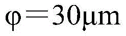 In other words, the depth of focus P is obtainedf=180μm。
Indeed, according to the present description, when the matrix array 23 is formed by a row of elementary detectors, the focal spot will probably cover a set of at least two elementary detectors in juxtaposition, whereas when the matrix array 23 is formed by a plurality of rows of elementary detectors, the focal spot will probably cover a set of at least four juxtaposed basesThe detector is provided. Since the imaging apparatus according to the present specification is intended to detect a plurality of wavelengths, it will be possible to use the minimum detection wavelength λminTo estimate the diameter of the diffraction spot And depth of focus.
As shown in fig. 2B, the matrix array 24 of metal-dielectric guided-mode resonance elementary filters is arranged in front of the detection matrix array 23 at a given distance d (for example less than the depth of focus), which makes it possible to avoid excessive divergence of the light beam with respect to each elementary filter.
Furthermore, the dimensions of the elementary filters are chosen such that each elementary focus formed at each point of the image field covers at least two elementary filters optimized for bandpass transmission in a spectral band centered at two different central wavelengths equal to the two detection wavelengths. At each elementary focal point, the elementary detectors therefore receive the filtered luminous flux in a spectral band centred on the different detection wavelengths.
For example, a schematic diagram of a two-dimensional matrix array 24 of elementary filters 24i is shown in fig. 2B. In this example, a zone Zi formed by 4 elementary filters can be defined, each optimized for detection in a spectral band centered on a different detection wavelength. In practice, the focal point of the imaging optics formed on the filter matrix array 24 and calculated, for example, using the minimum detection wavelength will likely cover a circular area inscribed in the frame Zi.
In practice, as shown in FIG. 2B, the size of the fundamental filter may be substantially the same as the size of the fundamental detector. However, it is also quite possible that the basic filter is slightly larger or smaller than the basic detector.
For example, the elementary filters have such dimensions that they cover a set of two elementary detectors (in the case of a 1D detection strip) or a set of 4 elementary detectors (in the case of a 2D detection matrix array), as long as the elementary filter matrix array is in the depth of focus of the imaging optics and in the elementary focal points, there are at least two elementary filters adapted to transmit in spectral bands centered on two different detection wavelengths.
In general, it is possible to define zones Zi formed by a greater number of elementary filters, which are identical or different, but each zone Zi comprising at least two elementary filters optimized for bandpass transmission in a spectral band centered at two different central wavelengths equal to the two detection wavelengths. The basic filters can be arranged in each zone Zi in a given arrangement. The zones Zi may all be the same, as in the example of FIG. 2B. Advantageously, the focal point is small enough to be accommodated in one zone Zi so that there is no "overflow" from one zone to another. For example, the focal point is circular and inscribed in one zone Zi.
As previously mentioned, a metal-dielectric guided-mode resonance (GMR) fundamental filter comprises a waveguide made of a dielectric material and at least one metal grating for coupling an incident wave to a guided mode of the waveguide, the metal grating being structured in a given pattern that repeats with a given period. Thus, even when the size of the elementary filter is substantially equal to the size of the elementary detector, as shown in fig. 2B, the elementary filter will likely be slightly larger or smaller than the elementary detector, since the size of the elementary filter is actually a multiple of the size of the pattern of the metal grating, with a difference smaller than the detection wavelength.
As shown in FIG. 2A, the basic filter 24i receives the converging light beam F0,F1The convergence of the light beam (beam F1) is greater at the field edge than the convergence of the light beam (beam F0) at the field center.

Wherein n ispixIs the maximum number of detection pixels (in one dimension), and tpixIs the pitch of the pixel.
For example, the number of pixel detections in a row is npix640, pixel pitch t pix15 μm, a diameter D of the imaging optics of 25mm and a focal length F of 50mm, a field edge angle α of 19 °is obtained
Thus, all or some of the fundamental filters, particularly the fundamental filters positioned at the field edges, will likely have an angular acceptance greater than or equal to the field edge angle of the device.
Various metal dielectric Guided Mode Resonance (GMR) fundamental filters known in the art may be used to implement an infrared multispectral imaging device according to the present description.
Sizing of the infrared spectrum filtered GMR filters in a multispectral imaging device according to the present description will likely include the following steps.
Defining the detection wavelength lambda of the detection spectral band at the detection wavelength considered according to the applicationdiAnd a width Δ λ i. For example, for the detection of specific chemical substances it may be advantageous to find narrow detection spectral bandwidths (narrower than 0.5 μm), while for other applications, for example for evaluating emissivity for a body, it may be advantageous to find broader detection spectral bandwidths (greater than 1 μm).
Detecting the characteristics of the matrix array: detecting strips or two-dimensional matrix arrays, number of pixels in each direction (n)pix) And size of one pixel (t)pix) And is also set according to the application.
The optical geometry of the device, in particular the number of openings N of the imaging optics and the focal length F, is chosen according to the scene to be observed, the detector (spatial resolution) and the maximum capacity required of the device.
How to determine the wavelength λ of detection sought is defined belowdiThe width Δ λ i of the detection band at the detection wavelength under consideration and the optical geometry of the detection device are detected to select and size the fundamental filter. In particular, one or more types may be determined in a given matrix array of elementary filtersA filter (DMG, diatomic, etc.), which will be described later.
For each type of filter, it is sought to determine the geometric parameters of the filter which allow achieving the optical characteristics sought for the filter, i.e. the maximum transmission TmaxResonant wavelength lambdarA resonance width Δ λ, and a sum angle acceptance Δ θ. In fact, with transmission TmaxSeeking resonant wavelength lambda corresponding to the central wavelength of the maximum transmission spectral bandrWill be equal to the detection wavelength lambdadi. The sought resonance width Δ λ, corresponding to the width at half maximum of the spectral response in transmission of the filter, will be equal to the width Δ λ of the detection spectral bandiAnd the angular acceptance Δ θ sought will likely be defined in terms of the field edge angle α of the device (see equation (3) above).
With respect to the angular acceptance Δ θ of the fundamental filter, it may be advantageous to select the angular acceptance to be greater than the field edge angle α for all filters of the matrix array or at least some filters at the field edge if the angular acceptance Δ θ is less than the field edge angle α, then the filter continues to operate, but its efficiency is reduced, due to the fact that at resonance TmaxThe transmission at is reduced and the quality factor Qi ═ λdi/ΔλiMay be degraded.
Once the type of filter is selected, determining the parameters of the fundamental filter may include the steps of: (1) selecting a first parameter, (2) simulating transmission as a function of wavelength and simulating transmission as a function of angle of incidence by numerical simulation, and (3) modifying the parameter in accordance with the results of the simulation.
For step (2) of verifying the first parameter by numerical simulation, a simulation of the transmission of the filter for the converging light beam may be performed. Which includes decomposing an incident converging beam into plane waves having different incident angles, simulating propagation of each of the substantially plane waves, and summing the substantially plane waves after propagation. However, the applicant has demonstrated that simulations of the transmission of the filter for "plane waves" can be used, since the parameters for plane waves obtained with simplified digital simulations are substantially similar to those obtained by simulations on the transmission of the converging light beam, as long as the angle of incidence of the waves remains within the angular tolerance range of the filter.
In any case, any known method can be used to simulate the response of the fundamental filter to incident electromagnetic waves. For example, modal computational methods such as Rigorous Coupled Wave Analysis (RCWA) may be used, which is described, for example, in josa 12,1068(1995) to m.g. moharam et al. May also be used, for example, as implemented in COMSOL Finite Element Methods (FEM) in software packages or implemented in
 Finite difference time domain method (FDTD) in software packages. The curves given in the remainder of this description are calculated using modal calculation methods, more specifically assuming plane waves and one-dimensional patterns (slits), using for
 Hugonin and P.Lanne, regenerative software for marking analysis, Institut d' Optique, Orsay, France (2005)).
As previously mentioned, in the context of the present description, for a given resonance wavelength λrThe metallodielectric guided-mode resonance fundamental filter optimized for bandpass transmission in the central spectral band comprises a layer (refractive index n) made of a dielectric material forming a waveguide capable of supporting only a single mode at said wavelengthdAnd a thickness td) And at least one metal diffraction grating (refractive index n)mAnd has a thickness tm) Constructed in a given pattern that repeats with a given period (p) less than the resonance wavelength. The diffraction grating is adapted to couple incident wavelengths at resonant wavelengths to guided modes. The pattern may comprise one or more openings of a given size, which may be two-dimensional (e.g. cross or circular openings) or one-dimensional (slits). The opening is filled with a dielectric material, which may be ambient air or another dielectric material,e.g. the dielectric material forming the waveguide or the dielectric material forming the substrate, depending on the different types of filters.
Three examples of the metallodielectric guided-mode resonance fundamental filter design for implementing the multispectral imaging device according to the present description are given below. These examples are not limiting, and other geometries may be used to implement the guided mode resonance fundamental filter. In each case, a similar method can be applied to define the parameters of the filter.
A first example is described with reference to fig. 3A-3C.
In fig. 3A, only one pattern of a basic filter 30 of size p has been shown. In practice, the basic filter comprises a repetition of the pattern thus shown, to form a diffraction grating having a period p.
The basic filter 30 shown in fig. 3A is of the suspended double metal grating ("DMG") type. Which comprises forming at a resonance wavelength lambdarA layer 31 of dielectric material supporting only single mode waveguides, and two metal diffraction gratings 32,33 arranged on either side of the layer of dielectric material, the DMG being suspended in a fluid such as air or a vacuum. Each metal grating is constructed in a given pattern that repeats with a given period p that is less than the resonant wavelength. More specifically, in the example of fig. 3A, the first metal grating 32 includes a grating having a respective width a1And a2And the second metal grating 33 comprises a pattern with a corresponding width a which is the same as the width of the slits of the pattern of the first grating1And a2Of the two slits 331, 332.
In the example of fig. 3A, the metal grating is referred to as a "diatomic" because each pattern thereof includes two slits having different widths. Diatomic DMG base filters of this type are described, for example, in the document published by e.sakat et al in 2013. Note, however, that while these filters are advantageous from an angular acceptance perspective, multispectral imaging devices employing "monatomic" suspended DMG base filters, i.e., filters in which the pattern of the metal diffraction grating includes only one slit, may also be designed, such as described in c.tardieu et al, Optics Letters 40, 4 (2015).
In the step (1) of determining the first parameter, the thickness and the refractive index t of the waveguide are first selectedgAnd ng。tgAnd ngIs selected to be small enough to cause the waveguide to resonate at the desired resonant wavelength λrCan support only a single mode. Therefore, it follows the following conditions:

the period p and the dielectric constant n are then adjustedgSo that normally incident plane waves at resonant wavelengths diffract only the 3 rd order in the waveguide and only the 0 th order in free space (incident or transmitting medium). For this purpose, the known law of transmission gratings applies.
The width of the slit can then be adjusted, taking into account that, in this case, two slits (a) having different widths are sought1≠a2). A wide slit allows a high transmission at resonance but reduces the quality factor. To obtain a narrower resonance, a narrower slit is required.
In fact, the applicant has shown that, at the detection wavelengths of interest (for example between 3 μm and 5 μm), the parameters of the optical filter can be chosen in the range of the following values:
tmbetween λr100 and lambdarBetween/10;
P<λr;
a1<λr/4、a2<λr/4,a1≠a2;
dielectric materials, e.g. silicon carbide (SiC) or silicon nitride (SiN)
tdBetween λrA/20 and lambdarAnd/2.
For the spectral range at the highest wavelengths, e.g. in the range of 8-12 μm, the typical dimensions will naturally be larger.
In step (2), the optical characteristics of each filter having the first selection parameters are verified using numerical simulations.
For this purpose, the transmission spectrum of the filter is calculated to obtain the maximum transmission in the simulated wavelength range and its wavelength position (fig. 3B), which correspond respectively to the value T of the transmission at the resonance of the filtermaxAnd resonance wavelength lambdar. The full width at half maximum of the resonance Δ λ is also obtained. Also calculated at a determined wavelength λrThe transmittance of which varies with the angle of incidence of the plane wave. From which the angular tolerance of the filter, Δ θ, is derived, which corresponds to the angle at which the transmission drops to half its normal incidence value.
The curves shown in fig. 3A and 3B thus show the transmittance as a function of wavelength and the transmittance as a function of angle of incidence for a guided mode resonance filter such as that shown in fig. 3A with the following parameters:
period p is 3 μm, a1=0.2μm,a2=0.7μm,tm0.1 μm and td=0.65μm,nd2.15(SiN x) and nmGiven by the Drude model of gold.
Simulations of this filter give: lambda [ alpha ]r=4.01μm,Tmax75%, Δ θ 17 ° and Δ λ 120 nm.
Depending on the properties sought, the design filter step (3) may include modifying the parameters for optimization purposes. For example, a lower resonance wavelength can be obtained by reducing the period p. Greater angular tolerances can be achieved by increasing the index of the guide. A spectrally narrower resonance can be obtained by reducing the width of both slits. However, each time a parameter is modified to alter the value of one of the optical characteristics, the other parameter must be readjusted, otherwise there is a risk of degrading the other of the optical characteristics. Optimization algorithms may also be used to find the optimal parameters, such as Particle swarm optimization algorithms (Mehrdad Shokooh-Saremiand et al, Particle swarm optimization and its 5 application to the design differentiation mapping filters, Opti. Lett.32, 894 + 896 (2007)).
A second example is described with reference to fig. 4A to 4C.
In fig. 4A, as in fig. 3A, only one pattern of one basic filter 40 of size p is shown. In practice, the basic filter comprises a repetition of the pattern thus shown, to form a diffraction grating having a period p.
The basic filter 40 shown in fig. 4A is a diatomic bimetallic grating (DMG) filter having a substrate. Which comprises forming a dielectric layer capable of forming a resonant wavelength λrA layer 41 (thickness t) of dielectric material of a waveguide supporting only a single modeaRefractive index of nm) And two metal diffraction gratings 42, 43 (of thickness tm) disposed on either side of the layer of dielectric material1、tm1Refractive index of nm1、nm2). It also comprises a refractive index nsub(nsub<nd) In this example, a layer 41 made of a dielectric material and a metal diffraction grating 42 are deposited on the substrate 44. Each metal grating is constructed in a given pattern that repeats for each grating with a given period p that is less than the resonant wavelength. More specifically, in the example of fig. 4A, the first metal grating 32 comprises a grating having a respective width b1And b2And the second metal grating 43 comprises a pattern with a respective width of a'1And a'2The pattern of two slits 431, 432.
In practice, in order to obtain a first estimate of the parameter, with a view to obtaining the sought characteristic, one can start with a suspended DMG filter as shown in fig. 3A. An appropriate substrate is then selected and the width of the slit of the grating in contact with the substrate is adjusted. A substrate with the lowest possible refractive index and a waveguide with a high refractive index are sought to maintain a single mode waveguide. The period p is chosen such that, as for the suspended waveguide, only the 0 th order of propagation diffracted by the grating propagates through the substrate. In this example, in contrast to the example of fig. 3A, the width and/or thickness of the slits of grating 42 are different from the slits of grating 43 to compensate for the exponential rate change of the substrate. Such filters are described, for example, in Optics Express 23, 25(2015) by c.
As previously mentioned, although a diatomic metal grating is shown in the example of fig. 4A, it is also possible to optimize the parameters for a single-atom DMG filter on the substrate.
The curves shown in fig. 4A to 4B (step 2) are the curves shown in fig. 1 showing the transmittance as a function of wavelength and the transmittance as a function of angle of incidence for a guided mode resonance filter as shown in fig. 4A with the following parameters: period p 2 μm, a1=0.12μm,a2=0.62μm,b1=0.15μm,b2=0.65μm,tm1=0.1μm,tm2=0.05μm,td=0.6μm,ng2.84(SiC), and nmGiven by the Drude model of gold.
The simulation of this filter gives: lambda [ alpha ]r=3.98μm,Tmax92%, Δ θ 20 ° and Δ λ 160 nm.
As previously mentioned, step (3) of modifying the parameters may be performed to optimize the parameters according to the sought after characteristics.
A second example is described with reference to fig. 5A to 5C.
As shown in fig. 5A, only one pattern of one basic filter 50 of size p is shown, as in fig. 3A. In practice, the basic filter comprises a repetition of the pattern thus shown, to form a diffraction grating having a period p.
The basic filter 50 shown in fig. 5A is of the type having a single metallization on the front side and a substrate. Which comprises forming a dielectric layer capable of forming a resonant wavelength λrA layer 51 (thickness t) of dielectric material at which a waveguide supporting only a single mode is formeddRefractive index na) And two diffractive metal gratings 52, 33 (thickness t) arranged at the same side of the layer made of dielectric material at this timem1、tm2Refractive index nm). It also comprises a refractive index nsub(nsub<ng) On which base 54 a layer 51 of dielectric material is deposited (the substrate being on the side opposite to that carrying the grating). Each metal grating being constructed in a given pattern, the pattern being less than the resonance wavelength for each gratingThe given period p repeats. More specifically, in the example of FIG. 5A, the first metal grating 52 includes a grating having the same width b'1And the second metal grating 53 includes a pattern having a width a "1Of the individual slits 531.
Indeed, in order to obtain a first estimate of the parameter, with a view to obtaining the sought characteristic, one can start with a suspended DMG filter (however in a single atom configuration) as shown in fig. 3A. An appropriate substrate is then selected and the width and thickness of the individual slits of each grating are adjusted to vary the quality factor and angular tolerance.
The curves shown in fig. 5A and 5B (step 2) show the transmittance as a function of wavelength and the transmittance as a function of angle of incidence for a guided mode resonance filter such as that shown in fig. 5A with the following parameters: period p ═ 1.5 μm, a "1=0.2μm,b’1=0.1μm,tm1=0.1μm,tm2=0.13μm,td=0.63μm,nd2.15(SiNx), and nmGiven by the Drude model of gold.
The simulations give for this filter: lambda [ alpha ]r=3.89μm,Tmax70%, Δ θ 15 ° and Δ λ 320 nm.
As previously mentioned, step (3) of modifying the parameters may be performed to optimize the parameters according to the sought after characteristics.
The applicant has demonstrated that the above-described metal-dielectric GMR filter can operate with a converging light beam and over an area that detects the size of the pixels.
Thus, fig. 6A shows a cross-sectional view of a matrix array 24 of guided mode resonance elementary filters, which in this example comprise elementary filters 24A,24B Basic filter 24A,24BEach adapted to operate at a respective wavelength λA,λBResonant transmission is performed in the centered spectral band. In this example, the matrix array 24 is formed by a row of elementary filters and is adapted to the filtering required in an infrared multispectral imaging device equipped with elementary detector strips. However, it may equally be suitable for use in a 2D matrix array equipped with elementary detectorsThe required filtering basic filter 2D matrix array in the infrared multispectral imaging device. Each filter includes a diffraction grating formed by several periods of the pattern such that the size of the filter is substantially the same as the size of the pixel.
Filters have been investigated in focusing the beam F0Behavior of0Including the entire wavelength range, including the wavelength lambdaA,λB. The applicant has shown that at resonance the electric and magnetic fields in the waveguide are limited in their diffusion, the electromagnetic fields being located at the filter 24AWavelength λ ofAAnd is located at the filter 24BWavelength λ ofBTo (3). Thus, as the output of the filter matrix array, at the central wavelength λ, respectivelyAAnd λBTo obtain a light beam FaAnd Fb。
Thus, fig. 6B shows the result of a numerical simulation of calculating the magnetic field strength within the fundamental filter, which simulation was performed using a fundamental filter matrix array as shown in fig. 6A. For this simulation, each filter 24A,24BAre respectively aimed atA4 μm and λBA suspended diatomic DMG filter optimized for a resonance wavelength of 4.7 μm (as shown in fig. 3A). The inset box 30 in FIG. 6A shows in detail the filter 24 limited to one patternA. The characteristics of the filter are as follows. For the optical filter 24APeriod p ofA3 μm, cycle number 5, slit width a1A=0.2μm,a2A0.5 μm. For the optical filter 24BPeriod p ofA3.7 μm, cycle number 4, slit width a1B=0.1μm,a2B0.7 μm. For two filters 24A,24BThe simulation was performed with a layer made of a dielectric material formed of SiN and a metal grating made of Au. Furthermore, tmA=tmB0.1 μm, and tdA=tdB=0.65μm。
For the simulation, the half angle of the opening is 9 DEG and at the wavelength lambdaBOf the focused light beam F0The filter is illuminated. It has been found that the electromagnetic field is in fact a substantial factor in spite of the guided mode resonance filterIn filter B and only transmits the incident radiation.
A matrix array of metallodielectric guided-mode resonance elementary filters suitable for use in a multispectral imaging device according to the present description can be manufactured according to known methods, for example as described in the articles cited in the present description. The matrix array may be deposited on a substrate or suspended.
The basic filter matrix array may then be arranged in various ways in the vicinity of the basic detector matrix array. The basic filter matrix array may for example be arranged not to be adhesively adhered to the spacers. It can also be adhesively attached by a transparent glue in the filtering wavelength range. To prevent reflection at the interface of the substrate or glue, an anti-reflection layer may be added if necessary. The glue adhesion can be accomplished in a variety of ways. For example, the filter is flipped over and the upper portion with the grating is glued to the detector array. However, according to another example, in the case of an on-substrate filter with a typical thickness (greater than 300 μm), which is typically greater than the depth of focus, the base may be thinned and adhesively attached to the detector matrix array by mechanical polishing or chemical etching.
Although described with several detailed exemplary embodiments, it will be apparent to those skilled in the art that the infrared multispectral imaging device and method according to the present description include various variations, modifications, and improvements. It is to be understood that such variations, modifications and improvements are within the scope of the invention as defined in the appended claims.
Claims (10)
1. An infrared multispectral imaging device (20) adapted to detect at least a first detection wavelength and a second detection wavelength, comprising:
-a detection matrix array (23) comprising a set of elementary detectors (23i) of predetermined size forming an image field of given size;
-imaging optics (22) having a given number of openings (N) and a given focal length (F), said number and focal length being adapted to form a basic focal spot at each point of the image field, said focal spot covering a set of at least two juxtaposed basic detectors;
-a matrix array (24) of metal-dielectric guided-mode resonance elementary filters (24i), arranged in front of said detection matrix array (23) at a distance smaller than the depth of focus of said imaging optics, the dimensions of said elementary filters being chosen such that each elementary focus formed at each point of the image field covers at least two elementary filters optimized for bandpass transmission in a spectral band centered at two different central wavelengths equal to two of said detection wavelengths.
2. The infrared multispectral imaging device according to claim 1, wherein at least one of the elementary filters has an angular acceptance measured in a plane wave greater than or equal to a field edge angle of the device, wherein the field edge angle is defined as the angle of the largest oblique ray intended to reach the elementary detector matrix array with respect to a direction normal to the elementary detector matrix array.
3. The infrared multispectral imaging device according to any one of the preceding claims, wherein the size of each of the elementary filters is substantially equal to the size of one elementary detector.
4. The infrared multispectral imaging device according to any one of the preceding claims, wherein the elementary filters (24i) of the matrix array of elementary filters (24) are arranged in zones (Zi), each zone comprising at least two elementary filters optimized for bandpass transmission in a spectral band centered on two different central wavelengths and having a size greater than that of the focal point.
5. The infrared multispectral imaging device according to any one of the preceding claims, wherein the matrix array of elementary filters (24) comprises at least one DMG guided-mode resonance elementary filter comprising a waveguide made of dielectric material and two metal gratings located on either side of the waveguide made of dielectric material.
6. The infrared multispectral imaging device according to claim 5, wherein the DMG guided-mode resonance fundamental filter is suspended and the two metal gratings are identical.
7. The infrared multispectral imaging device according to claim 5, wherein the DMG guided-mode resonance elementary filter is deposited on a substrate made of dielectric material and the two metal gratings of the elementary filter are different.
8. The infrared multispectral imaging device according to any one of the preceding claims, wherein the matrix array of elementary filters comprises at least one guided-mode resonant elementary filter having a single metallization on its front face, the filter comprising a waveguide made of a dielectric material deposited on a substrate, and a bimetallic grating on the face opposite to the substrate.
9. The infrared multispectral imaging device according to any one of the preceding claims, wherein the matrix array of elementary filters (24) comprises at least one guided-mode resonance elementary filter of the "diatomic" type, wherein the at least one metal grating is in a pattern with at least two openings of different size.
10. An infrared multispectral imaging method adapted to detect at least one first detection wavelength and one second detection wavelength, comprising:
-forming an image of a scene by means of imaging optics having a given opening (N) and acquiring said image by means of a detection matrix array comprising a set of elementary detectors of predetermined size forming an image field of a given size, said imaging optics (22) forming, at each point of said image field, an elementary focus covering a set of at least two juxtaposed elementary detectors;
-filtering the light beams focused by the imaging optics by means of a matrix array (24) of metal-dielectric guided-mode resonance elementary filters, arranged in front of the detection matrix array (23) at a distance smaller than the depth of focus of the imaging optics so that each elementary focal point formed at each point of the image field covers at least two elementary filters optimized for bandpass transmission in a spectral band centered at two different central wavelengths equal to two of the detection wavelengths.
Applications Claiming Priority (3)
| Application Number | Priority Date | Filing Date | Title |
|---|---|---|---|
| FR1753017A FR3065132B1 (en) | 2017-04-06 | 2017-04-06 | DEVICE AND METHOD FOR MULTISPECTRAL IMAGING IN THE INFRARED |
| FR1753017 | 2017-04-06 | ||
| PCT/EP2018/058822 WO2018185265A1 (en) | 2017-04-06 | 2018-04-06 | Device and method for multispectral imaging in the infrared |
Publications (2)
| Publication Number | Publication Date |
|---|---|
| CN110914992A true CN110914992A (en) | 2020-03-24 |
| CN110914992B CN110914992B (en) | 2023-11-07 |
Family
ID=59859142
Family Applications (1)
| Application Number | Title | Priority Date | Filing Date |
|---|---|---|---|
| CN201880037340.8A Active CN110914992B (en) | 2017-04-06 | 2018-04-06 | Infrared multispectral imaging device and method |
Country Status (7)
| Country | Link |
|---|---|
| US (1) | US11171174B2 (en) |
| EP (1) | EP3607585B1 (en) |
| JP (1) | JP7396898B2 (en) |
| CN (1) | CN110914992B (en) |
| CA (1) | CA3059260A1 (en) |
| FR (1) | FR3065132B1 (en) |
| WO (1) | WO2018185265A1 (en) |
Cited By (2)
| Publication number | Priority date | Publication date | Assignee | Title |
|---|---|---|---|---|
| CN112558293A (en) * | 2020-11-26 | 2021-03-26 | 中国科学院上海微系统与信息技术研究所 | Compact common-path confocal infrared dual-waveband optical system and manufacturing method thereof |
| CN113701887A (en) * | 2021-05-19 | 2021-11-26 | 哈尔滨工业大学 | Multispectral temperature field measuring device based on ultrahigh-temperature transient target and temperature measuring method thereof |
Families Citing this family (9)
| Publication number | Priority date | Publication date | Assignee | Title |
|---|---|---|---|---|
| US11270049B2 (en) * | 2018-09-12 | 2022-03-08 | Siemens Industry Software Inc. | Internal channel network detections for 3D printing |
| US11933735B2 (en) * | 2019-03-29 | 2024-03-19 | Osaka University | Optical detection device, optical detection method, method for designing optical detection device, sample classification method, and defect detection method |
| RU2713716C1 (en) * | 2019-06-11 | 2020-02-06 | Закрытое акционерное общество "МНИТИ" (ЗАО "МНИТИ") | Method of generating signals of different-spectral television images |
| CN111323122A (en) * | 2020-03-11 | 2020-06-23 | 中国科学院国家空间科学中心 | A spaceborne multi-channel aurora spectral imaging device |
| CN111652820B (en) * | 2020-06-02 | 2023-05-23 | 昆明物理研究所 | Method, device and image processing system for correcting non-uniformity of infrared image stripes |
| FR3113954B1 (en) | 2020-09-10 | 2023-03-03 | Commissariat Energie Atomique | OPTICAL FILTERING DEVICE |
| CA3137651A1 (en) * | 2020-12-19 | 2022-06-19 | The Boeing Company | Combined multi-spectral and polarization sensor |
| CN113267257A (en) * | 2021-05-18 | 2021-08-17 | 苏州睿新微系统技术有限公司 | Infrared imaging module and infrared imager |
| WO2023228451A1 (en) * | 2022-05-27 | 2023-11-30 | 浜松ホトニクス株式会社 | Optical detector and spectroscopic measurement device |
Citations (6)
| Publication number | Priority date | Publication date | Assignee | Title |
|---|---|---|---|---|
| US20040108564A1 (en) * | 2002-12-05 | 2004-06-10 | Lockheed Martin Corporation | Multi-spectral infrared super-pixel photodetector and imager |
| WO2009106316A2 (en) * | 2008-02-29 | 2009-09-03 | Fraunhofer-Gesellschaft zur Förderung der angewandten Forschung e. V. | Multi-spectral sensor |
| EP2616855A1 (en) * | 2010-09-17 | 2013-07-24 | Office National D'etudes Et De Recherches Aérospatiales (ONERA) | Spectral band-pass filter having high selectivity and controlled polarization |
| US20130342680A1 (en) * | 2012-06-21 | 2013-12-26 | Providence Photonics, Llc | Multi-spectral infrared imaging system for flare combustion efficiency monitoring |
| US20160146989A1 (en) * | 2013-06-17 | 2016-05-26 | Centre Nationale de la Recherche Scientifique - CN RS | Angular optical filtering element for angular filtering having controlled angular selectivity |
| US20160349228A1 (en) * | 2015-05-29 | 2016-12-01 | Rebellion Photonics, Inc. | Hydrogen sulfide imaging system |
Family Cites Families (10)
| Publication number | Priority date | Publication date | Assignee | Title |
|---|---|---|---|---|
| US3971065A (en) | 1975-03-05 | 1976-07-20 | Eastman Kodak Company | Color imaging array |
| JPS6014464A (en) * | 1983-07-05 | 1985-01-25 | Mitsubishi Electric Corp | Infrared ray image pickup device |
| US7807951B1 (en) * | 2004-03-01 | 2010-10-05 | Raytheon Company | Imaging sensor system with staggered arrangement of imaging detector subelements, and method for locating a position of a feature in a scene |
| AU2007268027B2 (en) | 2006-05-22 | 2012-08-09 | Bruker Spatial Biology, Inc. | Systems and methods for analyzing nanoreporters |
| JP5300344B2 (en) | 2007-07-06 | 2013-09-25 | キヤノン株式会社 | Photodetection element, imaging element, photodetection method, and imaging method |
| JP5121764B2 (en) | 2009-03-24 | 2013-01-16 | 株式会社東芝 | Solid-state imaging device |
| US8759773B2 (en) * | 2012-04-18 | 2014-06-24 | Raytheon Company | Infrared spectrometer with enhanced readout speed |
| AU2013365772B2 (en) * | 2012-12-19 | 2017-08-10 | Basf Se | Detector for optically detecting at least one object |
| JP6584149B2 (en) | 2015-05-29 | 2019-10-02 | キヤノン株式会社 | Imaging device |
| US10795174B1 (en) * | 2016-10-13 | 2020-10-06 | Robert Magnusson | Flat-top narrow bandpass filters based on cascaded resonant gratings |
-
2017
- 2017-04-06 FR FR1753017A patent/FR3065132B1/en active Active
-
2018
- 2018-04-06 EP EP18716250.8A patent/EP3607585B1/en active Active
- 2018-04-06 WO PCT/EP2018/058822 patent/WO2018185265A1/en not_active Ceased
- 2018-04-06 JP JP2019555008A patent/JP7396898B2/en active Active
- 2018-04-06 CA CA3059260A patent/CA3059260A1/en active Pending
- 2018-04-06 US US16/603,174 patent/US11171174B2/en active Active
- 2018-04-06 CN CN201880037340.8A patent/CN110914992B/en active Active
Patent Citations (6)
| Publication number | Priority date | Publication date | Assignee | Title |
|---|---|---|---|---|
| US20040108564A1 (en) * | 2002-12-05 | 2004-06-10 | Lockheed Martin Corporation | Multi-spectral infrared super-pixel photodetector and imager |
| WO2009106316A2 (en) * | 2008-02-29 | 2009-09-03 | Fraunhofer-Gesellschaft zur Förderung der angewandten Forschung e. V. | Multi-spectral sensor |
| EP2616855A1 (en) * | 2010-09-17 | 2013-07-24 | Office National D'etudes Et De Recherches Aérospatiales (ONERA) | Spectral band-pass filter having high selectivity and controlled polarization |
| US20130342680A1 (en) * | 2012-06-21 | 2013-12-26 | Providence Photonics, Llc | Multi-spectral infrared imaging system for flare combustion efficiency monitoring |
| US20160146989A1 (en) * | 2013-06-17 | 2016-05-26 | Centre Nationale de la Recherche Scientifique - CN RS | Angular optical filtering element for angular filtering having controlled angular selectivity |
| US20160349228A1 (en) * | 2015-05-29 | 2016-12-01 | Rebellion Photonics, Inc. | Hydrogen sulfide imaging system |
Cited By (2)
| Publication number | Priority date | Publication date | Assignee | Title |
|---|---|---|---|---|
| CN112558293A (en) * | 2020-11-26 | 2021-03-26 | 中国科学院上海微系统与信息技术研究所 | Compact common-path confocal infrared dual-waveband optical system and manufacturing method thereof |
| CN113701887A (en) * | 2021-05-19 | 2021-11-26 | 哈尔滨工业大学 | Multispectral temperature field measuring device based on ultrahigh-temperature transient target and temperature measuring method thereof |
Also Published As
| Publication number | Publication date |
|---|---|
| EP3607585A1 (en) | 2020-02-12 |
| CA3059260A1 (en) | 2018-10-11 |
| JP2020520467A (en) | 2020-07-09 |
| US20200066782A1 (en) | 2020-02-27 |
| FR3065132B1 (en) | 2019-06-28 |
| FR3065132A1 (en) | 2018-10-12 |
| WO2018185265A1 (en) | 2018-10-11 |
| US11171174B2 (en) | 2021-11-09 |
| CN110914992B (en) | 2023-11-07 |
| EP3607585B1 (en) | 2025-10-01 |
| JP7396898B2 (en) | 2023-12-12 |
Similar Documents
| Publication | Publication Date | Title |
|---|---|---|
| CN110914992B (en) | Infrared multispectral imaging device and method | |
| US11506538B2 (en) | Optical filter, optical filter system, spectrometer and method of fabrication thereof | |
| CN111579497B (en) | Spectrometer on a chip | |
| CN111061070B (en) | Multifunctional array element based on super surface structure and multifunctional realization method | |
| US7772555B2 (en) | Plasmon coupling apparatus and method | |
| US20200363323A1 (en) | Spectrometer | |
| WO2019075335A1 (en) | Lens-free compound eye cameras based on angle-sensitive meta-surfaces | |
| US9627434B2 (en) | System and method for color imaging with integrated plasmonic color filters | |
| JP5954801B2 (en) | Mirror for Fabry-Perot interferometer and method of making the mirror | |
| CN109029726B (en) | Window integrated type spectrum/polarization imaging system | |
| US8094306B2 (en) | Micro ring grating spectrometer with adjustable aperture | |
| JP2019523910A (en) | Light field imaging device and method for depth acquisition and 3D imaging | |
| US10050075B2 (en) | Multi-layer extraordinary optical transmission filter systems, devices, and methods | |
| JP2010524012A (en) | Device for collecting and collecting electromagnetic energy and apparatus comprising at least one such device | |
| KR20070064336A (en) | Low height imaging system and related methods | |
| KR102612412B1 (en) | Imaging sensor and method of manufacturing the same | |
| KR20220091342A (en) | Optical device | |
| KR102640203B1 (en) | Optical device including slot and apparatus employing the optical device | |
| JP5037044B2 (en) | Color image sensor | |
| CN113820013A (en) | Transmission type super-structure surface multispectral imager based on Fabry-Perot cavity | |
| CN112229515A (en) | Optical filter-based spectral analysis module and analysis method | |
| CN113267257A (en) | Infrared imaging module and infrared imager | |
| He et al. | Metasurfaces and Multispectral Imaging | |
| WO2022076438A1 (en) | Systems and methods to redistribute field of view in spectroscopy | |
| JP2025071731A (en) | Optical filter array, multi-wavelength sensor, and two-color temperature measurement device |
Legal Events
| Date | Code | Title | Description |
|---|---|---|---|
| PB01 | Publication | ||
| PB01 | Publication | ||
| SE01 | Entry into force of request for substantive examination | ||
| SE01 | Entry into force of request for substantive examination | ||
| TA01 | Transfer of patent application right |
Effective date of registration: 20210402 Address after: Fa Guopalaisuoshi Applicant after: Fa Guoyuhangyuan Address before: Fa Guopalaisuoshi Applicant before: Fa Guoyuhangyuan Applicant before: CENTRE NATIONAL DE LA RECHERCHE SCIENTIFIQUE |
|
| TA01 | Transfer of patent application right | ||
| GR01 | Patent grant | ||
| GR01 | Patent grant |