CN110828411A - Multi-chip bonding post-bending type packaging structure and method - Google Patents
Multi-chip bonding post-bending type packaging structure and method Download PDFInfo
- Publication number
- CN110828411A CN110828411A CN201911136701.7A CN201911136701A CN110828411A CN 110828411 A CN110828411 A CN 110828411A CN 201911136701 A CN201911136701 A CN 201911136701A CN 110828411 A CN110828411 A CN 110828411A
- Authority
- CN
- China
- Prior art keywords
- chip
- circuit board
- bending
- flexible circuit
- pad
- Prior art date
- Legal status (The legal status is an assumption and is not a legal conclusion. Google has not performed a legal analysis and makes no representation as to the accuracy of the status listed.)
- Pending
Links
Images


Classifications
-
- H10W72/50—
-
- H10W70/05—
-
- H10W70/688—
-
- H10W90/701—
-
- H10W72/01551—
-
- H10W72/075—
-
- H10W72/701—
Landscapes
- Wire Bonding (AREA)
Abstract
本发明公开了一种多芯片邦定后弯折式封装结构及方法,涉及芯片封装技术领域,包括柔性线路板,所述柔性线路板的外侧表面位置处固定设置有焊盘线路,所述柔性线路板的内侧表面固定设置有焊盘面层,所述柔性线路板的内部位于焊盘线路与焊盘面层之间开设有导通孔,本发明利用柔性线路板可弯折的特点实现多芯片邦定后弯折封装,可以实现更小的封装尺寸,相比传统芯片封装工艺可增加芯片集成数量及减少芯片封装尺寸,根据各个芯片尺寸利用柔性线路板的侧面弯折空间增加封装的芯片数量,达到更高的封装空间利用率,利用柔性线路板行业的生产优势进行拼板大量生产,另外极大地减少了芯片焊盘邦定次数,提高了生产效率。
The invention discloses a multi-chip bonding and post-bending packaging structure and method, and relates to the technical field of chip packaging, including a flexible circuit board, a pad circuit is fixedly arranged on the outer surface of the flexible circuit board, and the flexible circuit board is The inner surface of the circuit board is fixedly provided with a pad surface layer, and the interior of the flexible circuit board is provided with a conduction hole between the pad circuit and the pad surface layer. The package size can be reduced by bending after setting. Compared with the traditional chip packaging process, it can increase the number of chips integrated and reduce the size of the chip package. According to the size of each chip, the side bending space of the flexible circuit board can be used to increase the number of packaged chips. Achieving higher utilization of packaging space, using the production advantages of the flexible circuit board industry for mass production of panels, and greatly reducing the number of chip pad bonding times and improving production efficiency.
Description
技术领域technical field
本发明涉及芯片封装技术领域,具体是一种多芯片邦定后弯折式封装结构及方法。The invention relates to the technical field of chip packaging, in particular to a multi-chip bonding and post-bending packaging structure and method.
背景技术Background technique
芯片作为集成电路的控制及信号转换、传输的核心器件被广泛应用于电子信息行业。因为芯片工作时必须与外界隔离,以防止空气中的杂质对芯片电路的腐蚀而造成芯片电气性能下降,封装后的芯片也更便于安装和运输,所以对芯片采用封装的方法进行保护和应用。随着电子信息技术的快速发展,将含有不同功能的多颗芯片集成封装在一个结构体中以节省电路板上空间实现整个集成电路的小型化成为重要的发展方向。As the core device of integrated circuit control, signal conversion and transmission, chips are widely used in the electronic information industry. Because the chip must be isolated from the outside world during operation to prevent the corrosion of the chip circuit caused by the impurities in the air, the electrical performance of the chip will be reduced, and the packaged chip will be easier to install and transport, so the chip is protected and applied by packaging. With the rapid development of electronic information technology, it has become an important development direction to integrate multiple chips with different functions into one structure to save space on the circuit board and realize the miniaturization of the entire integrated circuit.
目前被广泛应用于芯片封装领域的是Wire Bonding技术,使用金属丝(金线、铝线等),利用热压或超声能源,完成微电子器件中固态电路内部互连接线的连接,即芯片与电路或金属引线框架之间的连接,该技术中产品生产受打金属线效率限制,由于打线工序只能逐个焊盘进行生产,效率低,打线工艺成本高,另外芯片只能焊盘面向上进行排列,在进行多芯片集成封装时需要的封装尺寸大,难以适应电子产品小型化、轻薄化的市场需求,因此,本领域技术人员提供了一种多芯片邦定后弯折式封装结构及方法。At present, Wire Bonding technology is widely used in the field of chip packaging. It uses metal wires (gold wires, aluminum wires, etc.), and uses thermal pressure or ultrasonic energy to complete the connection between the internal interconnections of solid-state circuits in microelectronic devices. The connection between circuits or metal lead frames. In this technology, the production of products is limited by the efficiency of metal wire bonding. Since the wire bonding process can only be produced one by one pad, the efficiency is low, and the cost of the wire bonding process is high. In addition, the chip can only have the pads facing up. For arrangement, the package size required for multi-chip integrated packaging is large, and it is difficult to meet the market demand for miniaturization and thinning of electronic products. method.
发明内容SUMMARY OF THE INVENTION
本发明的目的在于提供一种多芯片邦定后弯折式封装结构及方法,以解决上述背景技术中提出产品生产受打金属线效率限制,由于打线工序只能逐个焊盘进行生产,效率低,打线工艺成本高,另外芯片只能焊盘面向上进行排列,在进行多芯片集成封装时需要的封装尺寸大,难以适应电子产品小型化、轻薄化的市场需求的问题。The purpose of the present invention is to provide a multi-chip bonded and folded packaging structure and method, so as to solve the problem that the production of products proposed in the above-mentioned background technology is limited by the efficiency of metal wire bonding. Since the wire bonding process can only be produced one by one The cost of the wire bonding process is high. In addition, the chips can only be arranged with the pads facing up. The package size required for multi-chip integrated packaging is large, and it is difficult to meet the market demand for miniaturization and thinning of electronic products.
为实现上述目的,本发明提供如下技术方案:To achieve the above object, the present invention provides the following technical solutions:
一种多芯片邦定后弯折式封装结构,包括柔性线路板,所述柔性线路板的外侧表面位置处固定设置有焊盘线路,所述柔性线路板的内侧表面固定设置有焊盘面层,所述柔性线路板的一端设置IC1弯折端子,所述柔性线路板的另一端设置有IC34弯折端子,所述柔性线路板的中间位置处设置有IC2绑定端,所述IC1弯折端子的侧面固定设置有IC1芯片,所述IC2绑定端的侧面固定设置有IC1芯片,所述IC34弯折端子的侧面固定设置有IC3 芯片,所述IC34弯折端子的侧面靠近IC3芯片的一侧位置处固定设置有IC4芯片。A multi-chip bonded and folded packaging structure includes a flexible circuit board, a pad circuit is fixedly arranged on the outer surface of the flexible circuit board, and a pad surface layer is fixedly arranged on the inner surface of the flexible circuit board, One end of the flexible circuit board is provided with an IC1 bending terminal, the other end of the flexible circuit board is provided with an IC34 bending terminal, the middle position of the flexible circuit board is provided with an IC2 binding terminal, and the IC1 bending terminal is provided The side of the IC34 is fixedly provided with an IC1 chip, the side of the IC2 binding end is fixedly provided with an IC1 chip, the side of the IC34 bending terminal is fixedly provided with an IC3 chip, and the side of the IC34 bending terminal is close to the side of the IC3 chip. An IC4 chip is fixed at the place.
作为本发明进一步的方案:所述柔性线路板的内部位于焊盘线路与焊盘面层之间位置处开设有导通孔。As a further solution of the present invention, a via hole is opened inside the flexible circuit board at a position between the pad circuit and the pad surface layer.
作为本发明进一步的方案:所述柔性线路板的外侧位置处固定设置有封胶层。As a further solution of the present invention, a sealing layer is fixedly arranged at an outer position of the flexible circuit board.
作为本发明进一步的方案:所述IC1弯折端子与IC2绑定端之间位置处设置有IC5弯折端子,所述IC34弯折端子与IC2绑定端之间位置处设置有IC6弯折端子。As a further solution of the present invention: an IC5 bending terminal is provided at the position between the IC1 bending terminal and the IC2 binding end, and an IC6 bending terminal is set at the position between the IC34 bending terminal and the IC2 binding end .
作为本发明进一步的方案:所述IC5弯折端子的侧面固定设置有IC5芯片,所述IC6弯折端子的侧面固定设置有IC6芯片。As a further solution of the present invention, an IC5 chip is fixedly disposed on the side surface of the IC5 bending terminal, and an IC6 chip is fixedly disposed on the side surface of the IC6 bending terminal.
作为本发明进一步的方案:一种多芯片邦定后弯折式封装方法,包括以下步骤:As a further solution of the present invention: a multi-chip bonding-back bending packaging method, comprising the following steps:
Sp1:将多颗芯片的焊盘连接线路进行拼板设计,将柔性线路板设计为双面板结构,其中一面为焊盘面层,另一面为芯片邦定的焊盘线路,两面的电气功能连接通过导通孔实现,柔性线路板两侧弯折端子长度根据弯折半径、芯片位置等要求计算确定;Sp1: Assemble the pad connection lines of multiple chips, and design the flexible circuit board as a double-sided structure. One side is the pad surface layer, and the other side is the pad circuit for chip bonding. The electrical functions on both sides are connected through The via hole is realized, and the length of the bent terminals on both sides of the flexible circuit board is calculated and determined according to the requirements of the bending radius and the position of the chip;
Sp2:将各个芯片邦定至柔性线路板的焊盘线路对应区域上,根据各个芯片尺寸利用柔性线路板的侧面弯折空间增加封装的芯片数量;Sp2: Bond each chip to the corresponding area of the pad circuit of the flexible circuit board, and use the side bending space of the flexible circuit board to increase the number of chips to be packaged according to the size of each chip;
Sp3:对柔性线路板拼板中邦定芯片后需要弯折的端子进行冲裁成型;Sp3: Punch out the terminals that need to be bent after bonding the chip in the flexible circuit board assembly;
Sp4:将冲裁成型的柔性线路板端子弯折至与邦定焊盘相反一面进行固定,根据设计的线路板弯折端子长度决定弯折顺序,弯折端子短的先进行弯折固定;Sp4: Bend the punched flexible circuit board terminal to the opposite side of the bonding pad for fixing, and determine the bending sequence according to the designed length of the bending terminal of the circuit board. The short bending terminal is bent and fixed first;
Sp5:对弯折后固定的芯片进行封胶处理,起到隔绝芯片与外部环境的保护作用;Sp5: Sealing the fixed chip after bending to protect the chip from the external environment;
Sp6:最后进行裂片处理,将封胶后的芯片拼板切割形成单颗芯片即完成芯片邦定后弯折封装设计。Sp6: Finally, the split processing is performed, and the encapsulated chip panel is cut to form a single chip to complete the bending and packaging design after the chip is bonded.
与现有技术相比,本发明的有益效果是:Compared with the prior art, the beneficial effects of the present invention are:
本发明利用柔性线路板可弯折的特点实现多芯片邦定后弯折封装,可以实现更小的封装尺寸,有利于实现电子元器件小型化,相比传统芯片封装工艺可增加芯片集成数量及减少芯片封装尺寸,能够根据各个芯片尺寸利用柔性线路板的侧面弯折空间增加封装的芯片数量,达到更高的封装空间利用率,利用柔性线路板行业的生产优势进行拼板大量生产,另外极大地减少了芯片焊盘邦定次数,提高了生产效率。The present invention utilizes the flexible circuit board's feature of being bendable to realize the multi-chip bonding and then bending package, which can realize smaller package size, is conducive to realizing the miniaturization of electronic components, and can increase the number of integrated chips and Reducing the size of the chip package, it is possible to use the side bending space of the flexible circuit board to increase the number of chips packaged according to the size of each chip, to achieve a higher utilization rate of packaging space, and use the production advantages of the flexible circuit board industry for mass production of panels. Greatly reduces the number of chip pad bonding and improves production efficiency.
附图说明Description of drawings
图1为本发明实施例一中封装结构弯折前的侧视结构示意图;FIG. 1 is a schematic side view of the package structure before bending in the first embodiment of the present invention;
图2为本发明中柔性线路板的侧视结构示意图;Fig. 2 is the side view structure schematic diagram of the flexible circuit board in the present invention;
图3为本发明实施例一中封装结构弯折后的侧视结构示意图;FIG. 3 is a schematic side view of the package structure after bending in
图4为本发明实施例一中封装结构封胶处理后的侧视结构示意图;4 is a schematic side view of the structure of the package structure after the encapsulation process in the first embodiment of the present invention;
图5为本发明实施例二中封装结构弯折后的结构示意图。FIG. 5 is a schematic structural diagram of the package structure after bending in the second embodiment of the present invention.
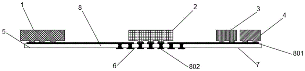
图中:1、IC1芯片;2、IC2芯片;3、IC3芯片;4、IC4芯片;5、IC1弯折端子;6、 IC2绑定端;7、IC34弯折端子;8、柔性线路板;801、焊盘线路;802、焊盘面层;803、导通孔;9、封胶层;10、IC5芯片;11、IC5弯折端子;12、IC6芯片;13、IC6弯折端子。In the figure: 1. IC1 chip; 2. IC2 chip; 3. IC3 chip; 4. IC4 chip; 5. IC1 bending terminal; 6. IC2 binding terminal; 7. IC34 bending terminal; 8. Flexible circuit board; 801, pad circuit; 802, pad surface layer; 803, via hole; 9, sealing layer; 10, IC5 chip; 11, IC5 bending terminal; 12, IC6 chip; 13, IC6 bending terminal.
具体实施方式Detailed ways
下面将结合本发明实施例,对本发明实施例中的技术方案进行清楚、完整地描述,显然,所描述的实施例仅仅是本发明一部分实施例,而不是全部的实施例。基于本发明中的实施例,本领域普通技术人员在没有做出创造性劳动前提下所获得的所有其他实施例,都属于本发明保护的范围。The technical solutions in the embodiments of the present invention will be clearly and completely described below with reference to the embodiments of the present invention. Obviously, the described embodiments are only a part of the embodiments of the present invention, rather than all the embodiments. Based on the embodiments of the present invention, all other embodiments obtained by those of ordinary skill in the art without creative efforts shall fall within the protection scope of the present invention.
实施例一:Example 1:
请参阅图1-4,本发明实施例中,一种多芯片邦定后弯折式封装结构,包括柔性线路板8,柔性线路板8的外侧表面位置处固定设置有焊盘线路801,柔性线路板8的内侧表面固定设置有焊盘面层802,柔性线路板8的一端设置IC1弯折端子5,柔性线路板8的另一端设置有IC34弯折端子7,柔性线路板8的中间位置处设置有IC2绑定端6,IC1弯折端子5的侧面固定设置有IC1芯片1,IC2绑定端6的侧面固定设置有IC1芯片2,IC34 弯折端子7的侧面固定设置有IC3芯片3,IC34弯折端子7的侧面靠近IC3芯片3的一侧位置处固定设置有IC4芯片4,柔性线路板8的内部位于焊盘线路801与焊盘面层802之间位置处开设有导通孔803,柔性线路板8的外侧位置处固定设置有封胶层9,起到隔绝芯片与外部环境的保护作用。Referring to FIGS. 1-4 , in an embodiment of the present invention, a multi-chip bonded and folded packaging structure includes a
实施例二:Embodiment 2:
请参阅图2和图5,本发明实施例中,一种多芯片邦定后弯折式封装结构,包括柔性线路板8,柔性线路板8的外侧表面位置处固定设置有焊盘线路801,柔性线路板8的内侧表面固定设置有焊盘面层802,柔性线路板8的一端设置IC1弯折端子5,柔性线路板8 的另一端设置有IC34弯折端子7,柔性线路板8的中间位置处设置有IC2绑定端6,IC1 弯折端子5的侧面固定设置有IC1芯片1,IC2绑定端6的侧面固定设置有IC1芯片2,IC34 弯折端子7的侧面固定设置有IC3芯片3,IC34弯折端子7的侧面靠近IC3芯片3的一侧位置处固定设置有IC4芯片4,柔性线路板8的内部位于焊盘线路801与焊盘面层802之间位置处开设有导通孔803,柔性线路板8的外侧位置处固定设置有封胶层9,IC1弯折端子5与IC2绑定端6之间位置处设置有IC5弯折端子11,IC34弯折端子7与IC2绑定端6 之间位置处设置有IC6弯折端子13,IC5弯折端子11的侧面固定设置有IC5芯片10,IC6 弯折端子13的侧面固定设置有IC6芯片12。Please refer to FIG. 2 and FIG. 5 , in an embodiment of the present invention, a multi-chip bonded and folded packaging structure includes a
根据各个芯片尺寸利用柔性线路板8的侧面弯折空间增加封装的芯片数量,达到更高的封装空间利用率。According to the size of each chip, the side bending space of the
实施例三:Embodiment three:
本发明实施例中,一种多芯片邦定后弯折式封装方法,包括以下使用步骤:In an embodiment of the present invention, a multi-chip bonding-back bending packaging method includes the following steps of use:
Sp1:将多颗芯片的焊盘连接线路进行拼板设计,将柔性线路板8设计为双面板结构,其中一面为焊盘面层802,另一面为芯片邦定的焊盘线路801,两面的电气功能连接通过导通孔803实现,柔性线路板8两侧弯折端子长度根据弯折半径、芯片位置等要求计算确定;Sp1: Assemble the pad connection circuits of multiple chips, and design the
Sp2:将各个芯片邦定至柔性线路板的焊盘线路801对应区域上,根据各个芯片尺寸利用柔性线路板8的侧面弯折空间增加封装的芯片数量;Sp2: Bond each chip to the area corresponding to the
Sp3:对柔性线路板8拼板中邦定芯片后需要弯折的端子进行冲裁成型;Sp3: Punch out the terminals that need to be bent after bonding the chip in the 8-piece assembly of the flexible circuit board;
Sp4:将冲裁成型的柔性线路板8端子弯折至与邦定焊盘相反一面进行固定,根据设计的线路板弯折端子长度决定弯折顺序,弯折端子短的先进行弯折固定;Sp4: Bend the 8 terminals of the punched flexible circuit board to the opposite side of the bonding pad for fixing, and determine the bending sequence according to the designed length of the bending terminals of the circuit board. The short bending terminals are bent and fixed first;
Sp5:对弯折后固定的芯片进行封胶处理,起到隔绝芯片与外部环境的保护作用;Sp5: Sealing the fixed chip after bending to protect the chip from the external environment;
Sp6:最后进行裂片处理,将封胶后的芯片拼板切割形成单颗芯片即完成芯片邦定后弯折封装设计。Sp6: Finally, the split processing is performed, and the encapsulated chip panel is cut to form a single chip to complete the bending and packaging design after the chip is bonded.
以上所述的,仅为本发明较佳的具体实施方式,但本发明的保护范围并不局限于此,任何熟悉本技术领域的技术人员在本发明揭露的技术范围内,根据本发明的技术方案及其发明构思加以等同替换或改变,都应涵盖在本发明的保护范围之内。The above are only preferred specific embodiments of the present invention, but the protection scope of the present invention is not limited thereto. The equivalent replacement or modification of the solution and its inventive concept shall be included within the protection scope of the present invention.
Claims (6)
Priority Applications (1)
| Application Number | Priority Date | Filing Date | Title |
|---|---|---|---|
| CN201911136701.7A CN110828411A (en) | 2019-11-19 | 2019-11-19 | Multi-chip bonding post-bending type packaging structure and method |
Applications Claiming Priority (1)
| Application Number | Priority Date | Filing Date | Title |
|---|---|---|---|
| CN201911136701.7A CN110828411A (en) | 2019-11-19 | 2019-11-19 | Multi-chip bonding post-bending type packaging structure and method |
Publications (1)
| Publication Number | Publication Date |
|---|---|
| CN110828411A true CN110828411A (en) | 2020-02-21 |
Family
ID=69556957
Family Applications (1)
| Application Number | Title | Priority Date | Filing Date |
|---|---|---|---|
| CN201911136701.7A Pending CN110828411A (en) | 2019-11-19 | 2019-11-19 | Multi-chip bonding post-bending type packaging structure and method |
Country Status (1)
| Country | Link |
|---|---|
| CN (1) | CN110828411A (en) |
Cited By (1)
| Publication number | Priority date | Publication date | Assignee | Title |
|---|---|---|---|---|
| CN114822234A (en) * | 2021-01-29 | 2022-07-29 | 京东方科技集团股份有限公司 | Flexible display module and preparation method thereof |
Citations (6)
| Publication number | Priority date | Publication date | Assignee | Title |
|---|---|---|---|---|
| US6102710A (en) * | 1992-08-05 | 2000-08-15 | Fujitsu Limited | Controlled impedance interposer substrate and method of making |
| US20010015487A1 (en) * | 2000-01-13 | 2001-08-23 | Forthun John A. | Stackable chip package with flex carrier |
| US20020050641A1 (en) * | 2000-08-22 | 2002-05-02 | Freeman Stacy L. | Apparatus and methods of semiconductor packages having circuit-bearing interconnect components |
| US20020137252A1 (en) * | 2001-03-21 | 2002-09-26 | Larson Charles E. | Folded interposer |
| CN105118827A (en) * | 2015-08-10 | 2015-12-02 | 成都锐华光电技术有限责任公司 | Three-dimensional chip stack packaging structure based on flexible substrate and packaging method |
| CN205946348U (en) * | 2016-08-30 | 2017-02-08 | 惠州新联兴实业有限公司 | Circuit board that can buckle |
-
2019
- 2019-11-19 CN CN201911136701.7A patent/CN110828411A/en active Pending
Patent Citations (6)
| Publication number | Priority date | Publication date | Assignee | Title |
|---|---|---|---|---|
| US6102710A (en) * | 1992-08-05 | 2000-08-15 | Fujitsu Limited | Controlled impedance interposer substrate and method of making |
| US20010015487A1 (en) * | 2000-01-13 | 2001-08-23 | Forthun John A. | Stackable chip package with flex carrier |
| US20020050641A1 (en) * | 2000-08-22 | 2002-05-02 | Freeman Stacy L. | Apparatus and methods of semiconductor packages having circuit-bearing interconnect components |
| US20020137252A1 (en) * | 2001-03-21 | 2002-09-26 | Larson Charles E. | Folded interposer |
| CN105118827A (en) * | 2015-08-10 | 2015-12-02 | 成都锐华光电技术有限责任公司 | Three-dimensional chip stack packaging structure based on flexible substrate and packaging method |
| CN205946348U (en) * | 2016-08-30 | 2017-02-08 | 惠州新联兴实业有限公司 | Circuit board that can buckle |
Cited By (3)
| Publication number | Priority date | Publication date | Assignee | Title |
|---|---|---|---|---|
| CN114822234A (en) * | 2021-01-29 | 2022-07-29 | 京东方科技集团股份有限公司 | Flexible display module and preparation method thereof |
| US12010798B2 (en) | 2021-01-29 | 2024-06-11 | Chengdu Boe Optoelectronics Technology Co., Ltd. | Flexible display module and manufacturing method thereof |
| US12495500B2 (en) | 2021-01-29 | 2025-12-09 | Chengdu Boe Optoelectronics Technology Co., Ltd. | Flexible display module and manufacturing method thereof |
Similar Documents
| Publication | Publication Date | Title |
|---|---|---|
| KR100445073B1 (en) | Dual die package | |
| WO2000033379A1 (en) | Semiconductor device, method of manufacture thereof, and electronic device | |
| CN103329263B (en) | Stitch bump stacking design for overall package size reduction for multiple stack | |
| TWI429043B (en) | Circuit board structure, packaging structure and method for making the same | |
| CN110828411A (en) | Multi-chip bonding post-bending type packaging structure and method | |
| CN1145211C (en) | Polycrystal chip semiconductor package structure and making method | |
| KR101959395B1 (en) | Semiconductor Devices and Methods of Fabricating the Same | |
| TW201208035A (en) | Multi-chip stacked assembly with ground connection of EMI shielding | |
| CN108807286A (en) | sensor LGA package structure | |
| CN201655790U (en) | A copper-aluminum wire hybrid bonding semiconductor chip package | |
| JP2008147226A (en) | Semiconductor device and manufacturing method thereof | |
| JP2716405B2 (en) | Semiconductor device and manufacturing method thereof | |
| JP2006066551A5 (en) | ||
| CN110838482A (en) | A kind of flexible circuit board bending packaging method | |
| CN106611752A (en) | Electrical connection structure between front surface and back surface of chip and manufacturing method thereof | |
| WO2017066896A1 (en) | Electrical connection structure between the front and rear of a chip, and manufacturing method therefor | |
| JP2002289741A (en) | Semiconductor device | |
| CN110828396A (en) | Multi-chip integrated embedded packaging method | |
| JP2023551331A (en) | Packaging modules and electronic devices | |
| JP4750076B2 (en) | Manufacturing method of semiconductor device | |
| CN212136446U (en) | WiFiSiP's bonding device | |
| CN216054687U (en) | Electric connection wire with chip | |
| CN101752278A (en) | Lead joint method in packaging of semiconductor and packaging structure | |
| CN101499431A (en) | Single-side bonding pad chip assembling method | |
| CN200941381Y (en) | Transistor structure of built-in circuits |
Legal Events
| Date | Code | Title | Description |
|---|---|---|---|
| PB01 | Publication | ||
| PB01 | Publication | ||
| SE01 | Entry into force of request for substantive examination | ||
| SE01 | Entry into force of request for substantive examination | ||
| RJ01 | Rejection of invention patent application after publication | ||
| RJ01 | Rejection of invention patent application after publication |
Application publication date: 20200221 |