CN110709692A - Apparatus and method for acquiring neural recordings - Google Patents
Apparatus and method for acquiring neural recordings Download PDFInfo
- Publication number
- CN110709692A CN110709692A CN201880036810.9A CN201880036810A CN110709692A CN 110709692 A CN110709692 A CN 110709692A CN 201880036810 A CN201880036810 A CN 201880036810A CN 110709692 A CN110709692 A CN 110709692A
- Authority
- CN
- China
- Prior art keywords
- microelectrode
- mea
- tip
- microelectrodes
- diameter
- Prior art date
- Legal status (The legal status is an assumption and is not a legal conclusion. Google has not performed a legal analysis and makes no representation as to the accuracy of the status listed.)
- Pending
Links
Images


Classifications
-
- G—PHYSICS
- G01—MEASURING; TESTING
- G01N—INVESTIGATING OR ANALYSING MATERIALS BY DETERMINING THEIR CHEMICAL OR PHYSICAL PROPERTIES
- G01N33/00—Investigating or analysing materials by specific methods not covered by groups G01N1/00 - G01N31/00
- G01N33/48—Biological material, e.g. blood, urine; Haemocytometers
- G01N33/483—Physical analysis of biological material
- G01N33/4833—Physical analysis of biological material of solid biological material, e.g. tissue samples, cell cultures
- G01N33/4836—Physical analysis of biological material of solid biological material, e.g. tissue samples, cell cultures using multielectrode arrays
-
- A—HUMAN NECESSITIES
- A61—MEDICAL OR VETERINARY SCIENCE; HYGIENE
- A61B—DIAGNOSIS; SURGERY; IDENTIFICATION
- A61B5/00—Measuring for diagnostic purposes; Identification of persons
- A61B5/24—Detecting, measuring or recording bioelectric or biomagnetic signals of the body or parts thereof
- A61B5/25—Bioelectric electrodes therefor
- A61B5/279—Bioelectric electrodes therefor specially adapted for particular uses
- A61B5/291—Bioelectric electrodes therefor specially adapted for particular uses for electroencephalography [EEG]
- A61B5/293—Invasive
-
- A—HUMAN NECESSITIES
- A61—MEDICAL OR VETERINARY SCIENCE; HYGIENE
- A61B—DIAGNOSIS; SURGERY; IDENTIFICATION
- A61B5/00—Measuring for diagnostic purposes; Identification of persons
- A61B5/68—Arrangements of detecting, measuring or recording means, e.g. sensors, in relation to patient
- A61B5/6846—Arrangements of detecting, measuring or recording means, e.g. sensors, in relation to patient specially adapted to be brought in contact with an internal body part, i.e. invasive
- A61B5/6847—Arrangements of detecting, measuring or recording means, e.g. sensors, in relation to patient specially adapted to be brought in contact with an internal body part, i.e. invasive mounted on an invasive device
- A61B5/685—Microneedles
-
- G—PHYSICS
- G01—MEASURING; TESTING
- G01N—INVESTIGATING OR ANALYSING MATERIALS BY DETERMINING THEIR CHEMICAL OR PHYSICAL PROPERTIES
- G01N27/00—Investigating or analysing materials by the use of electric, electrochemical, or magnetic means
-
- A—HUMAN NECESSITIES
- A61—MEDICAL OR VETERINARY SCIENCE; HYGIENE
- A61B—DIAGNOSIS; SURGERY; IDENTIFICATION
- A61B2503/00—Evaluating a particular growth phase or type of persons or animals
- A61B2503/42—Evaluating a particular growth phase or type of persons or animals for laboratory research
-
- A—HUMAN NECESSITIES
- A61—MEDICAL OR VETERINARY SCIENCE; HYGIENE
- A61B—DIAGNOSIS; SURGERY; IDENTIFICATION
- A61B2562/00—Details of sensors; Constructional details of sensor housings or probes; Accessories for sensors
- A61B2562/02—Details of sensors specially adapted for in-vivo measurements
- A61B2562/0209—Special features of electrodes classified in A61B5/24, A61B5/25, A61B5/283, A61B5/291, A61B5/296, A61B5/053
-
- A—HUMAN NECESSITIES
- A61—MEDICAL OR VETERINARY SCIENCE; HYGIENE
- A61B—DIAGNOSIS; SURGERY; IDENTIFICATION
- A61B2562/00—Details of sensors; Constructional details of sensor housings or probes; Accessories for sensors
- A61B2562/02—Details of sensors specially adapted for in-vivo measurements
- A61B2562/028—Microscale sensors, e.g. electromechanical sensors [MEMS]
-
- A—HUMAN NECESSITIES
- A61—MEDICAL OR VETERINARY SCIENCE; HYGIENE
- A61B—DIAGNOSIS; SURGERY; IDENTIFICATION
- A61B2562/00—Details of sensors; Constructional details of sensor housings or probes; Accessories for sensors
- A61B2562/04—Arrangements of multiple sensors of the same type
- A61B2562/046—Arrangements of multiple sensors of the same type in a matrix array
Landscapes
- Health & Medical Sciences (AREA)
- Life Sciences & Earth Sciences (AREA)
- Engineering & Computer Science (AREA)
- Physics & Mathematics (AREA)
- Biomedical Technology (AREA)
- General Health & Medical Sciences (AREA)
- Pathology (AREA)
- Biophysics (AREA)
- Molecular Biology (AREA)
- Chemical & Material Sciences (AREA)
- Veterinary Medicine (AREA)
- Surgery (AREA)
- Public Health (AREA)
- Medical Informatics (AREA)
- Animal Behavior & Ethology (AREA)
- Heart & Thoracic Surgery (AREA)
- Analytical Chemistry (AREA)
- Immunology (AREA)
- General Physics & Mathematics (AREA)
- Biochemistry (AREA)
- Optics & Photonics (AREA)
- Medicinal Chemistry (AREA)
- Food Science & Technology (AREA)
- Urology & Nephrology (AREA)
- Hematology (AREA)
- Chemical Kinetics & Catalysis (AREA)
- Electrochemistry (AREA)
- Measurement And Recording Of Electrical Phenomena And Electrical Characteristics Of The Living Body (AREA)
Abstract
Description
技术领域technical field
本公开涉及微电极领域。特别地是,本公开涉及用于检测可电激发细胞或可电激发细胞网络的电活性的微电极及微电极阵列。The present disclosure relates to the field of microelectrodes. In particular, the present disclosure relates to microelectrodes and microelectrode arrays for detecting the electrical activity of electrically excitable cells or networks of electrically excitable cells.
背景技术Background technique
许多神经系统疾病的潜在机制仍然是未知的。这种知识的缺乏可能源于对神经元活动的有限了解,神经元活动的范围从单个可电激发细胞到复杂的可电激发细胞构成的网络(在本文中称为可激发细胞网络(ECN))。了解构成ECN的形成、维持和退性的基础电生理机制可能有助于解决各种神经系统疾病的原因和治疗。The underlying mechanisms of many neurological disorders remain unknown. This lack of knowledge may stem from a limited understanding of neuronal activity, which ranges from single electrically excitable cells to complex networks of electrically excitable cells (referred to herein as excitable cell networks (ECNs)) ). Understanding the underlying electrophysiological mechanisms that underlie the formation, maintenance, and degeneration of ECNs may help address the causes and treatments of various neurological disorders.
已知使用形成平面微电极阵列(平面式MEA)的平面微电极研究ECN。平面式MEA能够与ECN通过接口进行接合,用于研究受控细胞外环境内的同质神经元种群。还已知将海马脑部切片与平面式MEA通过接口进行接合,以研究完整的三维ECN,以企图模拟生物体体内发现的场景。在研究神经功能时,尤其是在尝试扰乱ECN内的连通性时,保持ECN是至关重要的。It is known to study ECN using planar microelectrodes forming planar microelectrode arrays (planar MEAs). The planar MEA can interface with the ECN to study homogeneous neuronal populations within a controlled extracellular environment. It is also known to interface hippocampal brain slices with planar MEAs to study complete three-dimensional ECNs in an attempt to mimic scenarios found in living organisms. Preserving the ECN is critical when studying neural function, especially when trying to perturb the connectivity within the ECN.
但是,由已知MEA(如平面式MEA)采集的记录中的信噪比(SNR)通常非常低,这可能会干扰进行长期实验的能力。对于各种研究(包括但不限于药物筛选),以及对于各种神经系统疾病(包括但不限于癫痫),了解大脑中的神经通路和电活动灶,都需要长期实验。如图1中所示,已知MEA的局限性可能归因于至少三个因素:However, the signal-to-noise ratio (SNR) in recordings acquired by known MEAs, such as planar MEAs, is often very low, which may interfere with the ability to perform long-term experiments. Long-term experiments are required for various studies (including but not limited to drug screening), and for various neurological diseases (including but not limited to epilepsy) to understand neural pathways and foci of electrical activity in the brain. As shown in Figure 1, the limitations of known MEAs can be attributed to at least three factors:
1)平面式MEA 10仅记录来自组织配制品12的外层13的神经活动,该组织配制品包括可电激发细胞网络,并且外层13具有更高数量的受损或死细胞,这些不太可能代表生物体内的ECN,生物体内的ECN被发现处在组织配制品12的未损坏的内层14内;1) The
2)受损的神经元释放出不同类型的离子(主要是钾离子),这些离子能够被平面式MEA 10检测到并产生信号伪影;和2) Damaged neurons release different types of ions (mainly potassium ions) that can be detected by the
3)组织配制品12还经常需要经温度控制的灌注系统,其使用灌注流体流16,以提供连续的营养物和氧气流,这能够在记录室的间隙20内以及电极10周围产生离子流18,该离子流产生进一步的电噪声(见图1)。3) The
总体而言,当使用平面微电极或平面式MEA时,很难记录ECN的长期活性。此外,由于所记录的神经元的生活力,使用平面式MEA采集的数据可能是令人怀疑的,这使对于数据的解译变得困难。Overall, it is difficult to record the long-term activity of ECNs when using planar microelectrodes or planar MEAs. Furthermore, data acquired using planar MEAs can be suspect due to the viability of the recorded neurons, making interpretation of the data difficult.
发明内容SUMMARY OF THE INVENTION
本公开的实施例涉及一种三维(3D)微电极,其包括导电的伸长主体,该伸长主体具有:能够电连接至记录系统的基座;与所述基座相对的尖端,其构造用以与可激发细胞网络(ECN)建立电连通;以及位于基座和尖端之间的伸长部分。可选地是,伸长部分覆盖有至少一层电绝缘体涂层,该电绝缘体涂层从基座延伸到尖端的附近。3D微电极构造用以与受试者的组织接触(或至少部分地穿透进入受试者的组织)(生物体外,离体或生物体内),以使尖端与ECN的一个或多个细胞电连通。电绝缘体涂层可以减少信号伪影,该信号伪影可能是由于穿过受试者的组织的外层而引起的。Embodiments of the present disclosure relate to a three-dimensional (3D) microelectrode comprising an electrically conductive elongated body having: a base capable of being electrically connected to a recording system; a tip opposite the base, configured for establishing electrical communication with an excitable cell network (ECN); and an elongated portion between the base and the tip. Optionally, the elongated portion is covered with at least one coating of electrical insulator extending from the base to the vicinity of the tip. The 3D microelectrode is configured to contact (or at least partially penetrate into) a subject's tissue (in vitro, ex vivo, or in vivo) to electrically energize the tip to one or more cells of the ECN. Connected. The electrical insulator coating can reduce signal artifacts that may be caused by passing through the outer layers of the subject's tissue.
本公开的其他实施例涉及一种微电极阵列(MEA),该微电极阵列(MEA)包括至少两个如上所述的能够电连接到至少一个记录系统的3D微电极。3D-MEA可以用于将多个3D微电极的尖端呈现为与ECN的一个或多个细胞进行电连通。可以选择性地制造3D-MEA的每个3D微电极,以使所有3D微电极的高度和直径的尺寸基本相同或者不同。可选地是,可以在制造过程中选择每个3D微电极的高度和直径的尺寸中的一个或两者,以便针对给定的生物体外、离体或生物体内的应用以最佳的方式设计3D-MEA。例如,位于3D-MEA特定区域内的3D微电极可能是更长的,用以更远地伸进受试者的组织配制品的特定区域中。位于3D-MEA特定区域内的其他3D微电极可能具有更大的直径,以便与受试者的组织配制品的特定区域建立更牢固耐久的电连通。Other embodiments of the present disclosure relate to a microelectrode array (MEA) comprising at least two 3D microelectrodes as described above that can be electrically connected to at least one recording system. The 3D-MEA can be used to present the tips of multiple 3D microelectrodes in electrical communication with one or more cells of the ECN. Each 3D microelectrode of the 3D-MEA can be selectively fabricated such that the height and diameter of all 3D microelectrodes are substantially the same or different dimensions. Optionally, one or both of the dimensions of the height and diameter of each 3D microelectrode can be chosen during fabrication to be optimally designed for a given in vitro, ex vivo or in vivo application 3D-MEA. For example, 3D microelectrodes located within specific regions of the 3D-MEA may be longer to extend further into specific regions of the subject's tissue formulation. Other 3D microelectrodes located within specific regions of the 3D-MEA may have larger diameters in order to establish stronger and durable electrical communication with specific regions of the subject's tissue formulation.
本公开的其他实施例涉及一种制造3D微电极和3D-MEA以创建多位点记录平台的方法,其允许在生物体外、离体和生物体内以较高信号信噪比对ECN的电活性进行高分辨率的长期记录,并且与已知的设备相比,其造成更少的组织损伤。可以选择性地制造作为3D-MEA一部分的每个3D微电极,以使得根据受试者的组织配制品的区域来选择高度和直径的尺寸,那些3D微电极旨在与该区域建立电连通。可选地是,也可以选择裸露出来的并且未涂覆在电绝缘体涂层中的每个3D微电极的尖端的量。另外,每个3D微电极的尖端的形状也可以在钝的、尖的或平坦的之间选择性地制造。可以根据受试者的组织配制品的区域来选择尖端的形状,3D微电极旨在与该区域建立电连通。Other embodiments of the present disclosure relate to a method of fabricating 3D microelectrodes and 3D-MEAs to create a multi-site recording platform that allows in vitro, ex vivo, and in vivo electroactivity of ECNs with higher signal-to-noise ratios High-resolution long-term recordings are performed and cause less tissue damage than known devices. Each 3D microelectrode that is part of a 3D-MEA can be selectively fabricated such that the size of the height and diameter is chosen according to the area of the subject's tissue formulation with which those 3D microelectrodes are intended to establish electrical communication. Optionally, the amount of tip of each 3D microelectrode that is exposed and not coated in the electrical insulator coating can also be selected. Additionally, the shape of the tip of each 3D microelectrode can also be selectively fabricated between blunt, pointed, or flat. The shape of the tip can be chosen according to the area of the subject's tissue formulation with which the 3D microelectrodes are designed to establish electrical communication.
本公开的其他实施例涉及一种制造3D-MEA的方法,该方法包括以下步骤:在基板上的电绝缘材料层之间限定两个或更多个导电焊盘。方法包括在上述两个或更多个焊盘上沉积导电材料以形成3D微电极的伸长部分的步骤。沉积步骤还包括以下一个或多个步骤:在上述两个或更多个焊盘中的每个焊盘上形成3D微电极的基底;选择基座上的3D微电极的高度;以及选择基座上的导电材料的直径。Other embodiments of the present disclosure relate to a method of fabricating a 3D-MEA, the method comprising the steps of defining two or more conductive pads between layers of electrically insulating material on a substrate. The method includes the step of depositing a conductive material on the two or more pads described above to form elongated portions of the 3D microelectrode. The depositing step further includes one or more of the following steps: forming a substrate for the 3D microelectrode on each of the two or more pads described above; selecting the height of the 3D microelectrode on the pedestal; and selecting the pedestal The diameter of the conductive material on.
已知的平面微电极和平面式微电极阵列(MEA)只能记录来自包含可电激发细胞的组织的外层的神经活动。相反,本公开的3D微电极和3D-MEA的能够选择的长度可以使3D微电极尖端更深地进入受试者的组织配制品内,并因此与未损坏的细胞建立电连通。另外,本公开的3D微电极的电绝缘的伸长部分和基座可以在提供结构支撑的同时减少被记录下来的来自局部环境内的离子运动的噪声。Known planar microelectrodes and planar microelectrode arrays (MEAs) can only record neural activity from the outer layers of tissue containing electrically excitable cells. In contrast, the selectable lengths of the 3D microelectrodes and 3D-MEAs of the present disclosure can allow the 3D microelectrode tip to penetrate deeper into the subject's tissue formulation and thus establish electrical communication with undamaged cells. Additionally, the electrically insulating elongated portions and bases of the 3D microelectrodes of the present disclosure can reduce the noise recorded from ion motion within the local environment while providing structural support.
在不受任何具体理论约束的情况下,本公开的实施例可用于增加对神经退行性疾病(诸如但不限于阿尔茨海默氏症、帕金森氏症和癫痫症)的了解和潜在治疗。本公开还可用于增加对受试者内的认知、情感和行为能力的了解。本公开的实施例还可用于控制神经假体,从而向患者提供反馈并允许开发出用于神经退行性疾病的个性化药物或疗法。将本公开的实施例用于研究也可用于药物筛选以及了解基本的脑功能,包括但不限于神经网络现象。Without being bound by any particular theory, embodiments of the present disclosure may be used to increase the understanding and potential treatment of neurodegenerative diseases such as, but not limited to, Alzheimer's, Parkinson's, and epilepsy. The present disclosure can also be used to increase understanding of cognitive, affective, and behavioral capabilities within a subject. Embodiments of the present disclosure may also be used to control neuroprostheses, thereby providing feedback to patients and allowing the development of personalized medicines or therapies for neurodegenerative diseases. The use of embodiments of the present disclosure for research can also be used for drug screening and understanding basic brain functions, including but not limited to neural network phenomena.
附图说明Description of drawings
在下面的详细描述中,本公开的这些和其他特征将变得更加显而易见,在下面的详细描述中参考了附图:These and other features of the present disclosure will become more apparent from the following detailed description, which refers to the accompanying drawings:
图1示出了微电极阵列的两个示意图,其中图1的(A)是定位在现有技术的平面式微电极阵列(平面式MEA)上的组织配制品的示意图;图1的(B)示出了根据本公开的实施例的三维微电极阵列(3D-MEA);Figure 1 shows two schematic views of a microelectrode array, wherein Figure 1(A) is a schematic view of a tissue formulation positioned on a prior art planar microelectrode array (planar MEA); Figure 1(B) A three-dimensional microelectrode array (3D-MEA) according to an embodiment of the present disclosure is shown;
图2是根据本公开的实施例的制造和使用3D-MEA的方法的两个示意图,其中图2的(A)至(G)示出了3D-MEA的制造方法中的步骤,而图(H)示出了使用3D-MEA的方法;2 is two schematic diagrams of a method of manufacturing and using a 3D-MEA according to an embodiment of the present disclosure, wherein (A) to (G) of FIG. 2 show steps in the method of manufacturing the 3D-MEA, and FIG. ( H) shows the method using 3D-MEA;
图3是根据本公开的实施例的包括3D微电极的3D-MEA的一系列照片,其中图3的A是MEA的照片;图3的B是九个3D微电极的比图3的A更特写的照片;而图3的C是一个3D微电极的尖端的扫描电子显微镜照片;3 is a series of photographs of a 3D-MEA including 3D microelectrodes according to an embodiment of the present disclosure, wherein A of FIG. 3 is a photograph of the MEA; B of FIG. 3 is a photograph of nine 3D microelectrodes more than A of FIG. 3 Close-up photo; while Figure 3C is a scanning electron microscope photo of the tip of a 3D microelectrode;
图4是用于包含ECN样品的组织配制品一起使用的图3的3D-MEA的两张照片,其中图4A是与记录系统集成一体的3D-MEA的照片;而图4B是位于3D-MEA上的组织配制品的照片;Figure 4 are two photographs of the 3D-MEA of Figure 3 for use with tissue preparations containing ECN samples, wherein Figure 4A is a photograph of the 3D-MEA integrated with a recording system; and Figure 4B is located on the 3D-MEA Photographs of tissue preparations on;
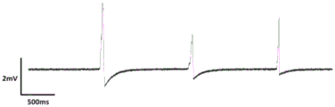
图5示出了使用图3的3D-MEA而从ECN样品中检测到的电活动的记录的示例;Figure 5 shows an example of a recording of electrical activity detected from an ECN sample using the 3D-MEA of Figure 3;
图6示出了使用图3的3D-MEA而从ECN样品中检测到的电活动的记录的另一示例;Figure 6 shows another example of a recording of electrical activity detected from an ECN sample using the 3D-MEA of Figure 3;
图7示出了用光学显微镜拍摄到的位于电极阵列上的急性海马脑部切片的照片。区域包括中脑(MD),丘脑(TH)(具有已识别的子区域T1、T2、T3、T4、T5、T6和T7,和海马(H)(具有已识别的子区域H1、H2、H3、H4和H5;Figure 7 shows a photo of an acute hippocampal brain slice on an electrode array taken with a light microscope. Regions include midbrain (MD), thalamus (TH) (with identified subregions T1, T2, T3, T4, T5, T6, and T7, and hippocampus (H) (with identified subregions H1, H2, H3) , H4 and H5;
图8示出记录到的丘脑子区域T1至T7内的电活动的示例;Figure 8 shows an example of recorded electrical activity in the thalamic brain regions T1 to T7;
图9示出记录到的海马子区域H1至H5内的电活动的示例;Figure 9 shows an example of recorded electrical activity within the hippocampal subregions H1 to H5;
图10是根据本公开的一个实施例的3D-MEA的俯视示意图;10 is a schematic top view of a 3D-MEA according to one embodiment of the present disclosure;
图11是图10中所示的3D-MEA的一个部分的俯视示意图;Figure 11 is a schematic top view of a portion of the 3D-MEA shown in Figure 10;
图12是图10中所示的3D-MEA的多个部分的两幅示意图,其中,图12的(A)是电极支撑焊盘和导线部的俯视示意图;而图12的(B)是图12的(A)中所示的焊盘的侧视图;12 is two schematic diagrams of parts of the 3D-MEA shown in FIG. 10 , wherein (A) of FIG. 12 is a schematic plan view of electrode support pads and lead portions; and (B) of FIG. 12 is a diagram of Side view of the pad shown in (A) of 12;
图13示出了在将MEA植入活动物大脑之后而获得的三组示例数据,其中图13的(A)示出了使用已知电极获得的电连通数据的示例;图13的(B)示出了使用根据本公开的3D-MEA获得的电连通数据的示例;而图13的(C)示出了动物大脑内的发作期(该发作期之后是发作后期)的证据;和Figure 13 shows three sample sets of data obtained following implantation of MEAs into a living animal brain, wherein Figure 13(A) shows an example of electrical connectivity data obtained using known electrodes; Figure 13(B) An example of electrical connectivity data obtained using a 3D-MEA according to the present disclosure is shown; while (C) of FIG. 13 shows evidence of a ictal phase (which is followed by a post-ictal phase) within the animal brain; and
图14是根据本公开的一个实施例的两个柔性3D-MEA的照片,其中一个基本是直的,而另一个处于弯曲姿势。14 is a photograph of two flexible 3D-MEAs, one of which is substantially straight and the other in a curved posture, according to one embodiment of the present disclosure.
具体实施方式Detailed ways
定义definition
除非另有定义,否则本文中使用的所有技术和科学术语具有与本公开所属领域的普通技术人员通常所理解的相同含义。Unless otherwise defined, all technical and scientific terms used herein have the same meaning as commonly understood by one of ordinary skill in the art to which this disclosure belongs.
如本文中所用,术语“约”是指与给定值相差约+/-10%。应当理解,无论是否特别提及,这种差总是包括在本文中提供的任何给定值内。As used herein, the term "about" means about +/- 10% from a given value. It should be understood that such differences are always included in any given value provided herein, whether or not specifically mentioned.
如本文中所用,术语“电连通”是指电信号的单向流动和/或电信号的双向交换。电信号的单向流动可起源于:至少一个可电激发细胞,根据本公开的三维(3D)微电极,或以上两者。电信号的双向交换是指通过3D微电极和至少一个可电激发细胞进行电信号的传输和接收。电连通还可以指在3D微电极和至少一个可电激发细胞之间的电信号的检测和/或传输。As used herein, the term "electrical communication" refers to the unidirectional flow of electrical signals and/or the bidirectional exchange of electrical signals. The unidirectional flow of electrical signals can originate from: at least one electrically excitable cell, a three-dimensional (3D) microelectrode according to the present disclosure, or both. The bidirectional exchange of electrical signals refers to the transmission and reception of electrical signals through the 3D microelectrode and at least one electrically excitable cell. Electrical communication can also refer to the detection and/or transmission of electrical signals between the 3D microelectrode and the at least one electrically excitable cell.
如本文中所用,术语“可电激发细胞”是指具有响应于电、化学或物理刺激而使带电离子穿过细胞膜传递的电势的细胞。在一些情况下,可电激发细胞可以以调节的方式去极化,以产生并传播一个或多个动作电位或端板电位。可电激励细胞的一些示例包括但不限于所有类型的神经细胞和肌肉细胞。As used herein, the term "electrically excitable cell" refers to a cell that has the potential to transmit charged ions across the cell membrane in response to electrical, chemical or physical stimulation. In some cases, electrically excitable cells can be depolarized in a regulated manner to generate and propagate one or more action potentials or endplate potentials. Some examples of electrically energizable cells include, but are not limited to, all types of nerve cells and muscle cells.
如本文中所用,术语“可激发细胞网络”和首字母缩略词“ECN”是指相互连接起来的多个可电激发细胞构成的网络,使得对网络内一个或多于一个的可电激发细胞的刺激将引起网络内的至少一个另外的可电激发细胞中的响应。至少一个另外的可电激发细胞的响应将包括带电离子穿过其细胞膜的传递和/或一个或多个细胞外信号分子的释放。As used herein, the term "excitable cell network" and the acronym "ECN" refer to a network of electrically excitable cells interconnected such that one or more than one electrically excitable cell within the network is Stimulation of a cell will elicit a response in at least one additional electrically excitable cell within the network. At least one additional response of the electrically excitable cell will include the transmission of charged ions across its cell membrane and/or the release of one or more extracellular signaling molecules.
如本文中所用,术语“组织配制品”是指受试者的组织,其包括一个或多个可电激发细胞和ECN的至少一部分。根据本公开的3D-MEA可以与组织配制品接触并与上述一个或多个可电激发细胞和ECN的至少一部分建立生物体外、离体或生物体内电连通。As used herein, the term "tissue formulation" refers to a tissue of a subject that includes one or more electrically excitable cells and at least a portion of the ECN. A 3D-MEA according to the present disclosure can be brought into contact with a tissue formulation and established in vitro, ex vivo, or in vivo electrical communication with at least a portion of the one or more electrically excitable cells and the ECN described above.
本公开涉及一种用于与单个可电激励细胞和/或可电激励细胞网络建立电连通的3D微电极210,在本文中将其称为可激发细胞网络(ECN)(见图1的(B))。在本公开的一些实施例中,3D微电极210包括导电的伸长主体204,其具有能够电连接到记录系统的基座202。3D微电极210还包括尖端206,其与基座202相对并且被构造用以建立与ECN的至少一部分的电连通。伸长部分204被限定在基座202和尖端206之间。基座202通常具有比伸长部分204更大的直径,并且伸长部分通常具有比基座202和尖端206更大的长度。通常,尖端206的形状为截头圆锥形,具有减小至细尖点的直径,该细尖点的直径比伸长部分204的直径小许多倍。基板102可以包括多个层(例如,放置在基板102和导电电极支撑焊盘109之间的额外材料104),其支撑每个3D微电极210。在制造过程中,这些多个层中的一些层或多个层的部分可被去除或降解。例如,可以将额外材料104放置在基板102上,该基板102为处在其上的一层或多层的不同材料(例如,形成焊盘109的导电材料层)提供结构支撑。在一些情况下,基板102是刚性的,并且在一些情况下,基板102是更柔性的。可以提供基板102上的上述另外的材料层,以允许将不同的材料(例如,构成焊盘109和导线105的不同的材料)附接到基板102。The present disclosure relates to a
伸长部分204可以覆盖有至少一层电绝缘体涂层208,该电绝缘体涂层208从基座202朝向尖端206延伸并延伸到尖端206的附近。3D微电极210的尖端206被构造用以建立与ECN的电连通。3D微电极210可以通过或不通过直接物理接触而建立与ECN的电连通。例如,在本公开的一些实施例中,将3D微电极210构造成至少部分地穿透进入到组织配制品12中(图2的H中示出),该组织配制品12包括可电激发细胞并且构成ECN的至少一部分。The
在本公开的一些实施例中,至少两个3D微电极210被构造成阵列,其在本文中称为3D微电极阵列(3D-MEA)212(在图1的(B)中示出)。3D-MEA 212可以与各种类型的组织配制品12一起使用,包括但不限于:生物体外组织配制品12,离体组织配制品12或生物体内组织配制品12。在本公开的一些实施方式中,3D-MEA212可用于与组织配制品12内的ECN建立电连通,以响应于电刺激、化学刺激或物理刺激来检测ECN的电活动的任何变化。在本公开的一些实施例中,3D-MEA 212能够建立用于刺激组织配制品12内的ECN的电连通。在本公开的一些实施例中,3D-MEA 212能够建立用于检测和刺激组织配制品12内的ECN的电连通。3D-MEA212的两个3D微电极210能够电连接到相同的记录系统。如图1的(B)中所示,单独的3D-MEA 212可以包括具有不同的长度和/或不同的直径的3D微电极210。这是因为能够基于本文中所述的方法选择性地制造给定的3D-MEA 212的每个单独的3D微电极210,并且能够基于3D-MEA 212的所期望的用途应用来单独选择每个3D微电极210的具体尺寸。In some embodiments of the present disclosure, at least two
图10示出了3D-MEA 212的一个实施例,其包括具有第一基板部分104A和第二基板部分104B的基板102。图10、图11和图12的(A)示出了3D-MEA 212的平面部分。第一基板部分104A包括一个或多个端子107,其被构造用以提供与发送器/接收器系统(未示出)的电连通。从每个端子107延伸出来的是导线部分105。导线部分从第一部分104A延伸到第二部分104B以及延伸到位于第二部分104B中的焊盘109。导线部分105是导电的,并且在给定的焊盘109上的每个3D微电极210和给定的端子107之间提供电连通。导线部分105可以通过一个或多个绝缘层而是绝缘的或是不绝缘的。每个焊盘109是3D-MEA 212的位置,3D微电极210的基座202在该位置上沉积于并附接到基板102。在一些实施例中,在一个端子107、一个导线部分105和一个焊盘109之间存在匹配关系。在另一实施例中,在一个端子107、一个导线部分105和两个或更多个焊盘109之间可能存在不匹配的关系。在其他实施例中,在多于一个的焊盘109(和其上面的3D微电极210)以及多于一个的端子107之间可存在电连通。FIG. 10 shows one embodiment of a 3D-
图14示出了3D-MEA 212的两个示例的照片,其中一个在焊盘109与第一基板部分104A之间处于弯曲姿势。Figure 14 shows photographs of two examples of the 3D-
在本公开的一些实施例中,部分104A、104B都不是柔性的。在本公开的一些实施例中,第一部分104A和第二部分104B之一或两者是柔性的。如本领域技术人员将理解的那样,使基板102的至少一个部分是柔性的对于在3D-MEA 212的3D微电极210和ECN之间建立最佳的物理接触或接近是有利的,该ECN是由组织配制品12的通常非平坦的柔性表面限定的。In some embodiments of the present disclosure, neither portion 104A, 104B is flexible. In some embodiments of the present disclosure, one or both of the first portion 104A and the second portion 104B are flexible. As those skilled in the art will appreciate, having at least a portion of the
如图10中所示,能够基于组织配制品12的性质来选择3D-MEA 212的设计,该组织配制品包含ECN,3D-MEA 212旨在与其进行电连通。如图10中所示,基板102可以具有大致T形,或者可以采取任何其他期望的形状。在图10、图11和图12中所示的非限制性示例中,第一部分104A和第二部分104B各自均限定在下表1中列出的各种尺寸。本领域技术人员将理解,表1中提供的尺寸仅作为示例提供。表1中提供的尺寸是根据使用3D-MEA 212来建立与大鼠脑部组织配制品的生物体外电连通的意图而进行选择的。但是,对于与不同的组织样品的其他用途,能够选择性地以比下表1中所列出的尺寸更大或更小的尺寸来制造3D-MEA212。例如,可以选择性地以比下表1中的尺寸更大的尺寸来制造意图与人类受试者一起使用的3D-MEA 212。As shown in Figure 10, the design of the 3D-
表1:根据本公开的一个实施例的3D-MEA的尺寸示例Table 1: Example dimensions of a 3D-MEA according to one embodiment of the present disclosure
(除非另有说明,否则为mm)。(mm unless otherwise stated).


在能够与生物体内ECN一起使用的3D-MEA 212的实施例中,能够将3D-MEA 212制造在柔性且生物相容的基板102上,该基板102被构造用以植入活生物体中。3D-MEA 212还能够被构造用以检测生物体内ECN的电活动和/或用以刺激生物体内ECN或其特定区域。In an embodiment of a 3D-
本公开的一些实施例涉及一种制作3D微电极210的制造方法和一种制作3D-MEA212的方法。3D微电极210(或者作为单独的3D微电极210或者作为3D-MEA 212的一部分)能够通过精确控制以下各项来单独制作:3D-MEA 212内的每个3D微电极210的高度和直径;被覆盖在电绝缘体材料208中的伸长部分204的长度;尖端206的长度;以及尖端206的形状。每个3D微电极210在3D-MEA 212内以及在基板102上的间距和位置。制造方法允许选择:用于制作3D微电极210的材料、电绝缘涂层208和在上面构建了3D-MEA 212的基板102的每一层的材料。制造方法还允许选择未被电绝缘涂层208覆盖的每个3D微电极210的表面面积以及这些未覆盖的部分在3D-MEA 212内的位置。Some embodiments of the present disclosure relate to a method of making a
如图2中所示,制造方法包括以下步骤:建立300第一层,该第一层由一种或多种材料104和导电材料组成,其在基板102上形成导电的电极支撑焊盘109。第一步骤的产物称为经涂覆的坯料100。制造方法的下一步骤是通过去除基板102的一层或多层而在经涂覆的坯料100上建立302一个或多个凹槽106。制造步骤的下一步骤是在凹槽之间定位304电绝缘材料108,以限定一个或多个焊盘109。或者,电绝缘材料108能够沉积在基板102上,然后从焊盘109的位置上基本去除。或者,电绝缘材料108层能够具有在其中限定出来的孔,然后能够利用已经在其上的焊盘109将该绝缘层粘附到基板102。绝缘层中的孔将与焊盘109对准。如图12的B中所示,可选地是,电绝缘材料108能够覆盖或重叠焊盘109的外周边缘。这种重叠在将3D微电极210沉积到焊盘109的同时提供一些额外的刚性支撑。As shown in FIG. 2 , the fabrication method includes the steps of creating 300 a first layer consisting of one or
制造方法的下一步是将导电材料沉积306在上述一个或多个焊盘109上。沉积306的步骤能够通过各种方法进行,包括但不限于:引线接合法、溅射、电沉积、蒸发、挤出、上述方法的组合或用以制作具有所期望的几何形状的导电材料的其他方法。沉积306的步骤可以进一步包括选择3D微电极210的伸长部分204的直径的步骤。例如,如果特定的3D微电极210旨在更深地穿透进入到组织配制品12的一部分中,那么该3D微电极210可以具有较小的直径,从而当该3D微电极移动通过组织配制品12时,其侵害性较小。在本公开的一些实施例中,每个伸长部分204的直径可以在以下范围内选择:在约1微米至1000微米之间。在本公开的一些实施例中,伸长部分204的直径可以被选择为在大约5微米与大约750微米之间的范围内。在本公开的一些实施例中,伸长部分204的直径在大约5和1000微米之间。The next step in the fabrication method is to deposit 306 a conductive material on one or more of the
沉积306的步骤包括形成基座202和选择3D微电极210的高度的步骤。长度的选择可以包括以下步骤:停止导电材料在焊盘109上沉积306并且/或者在沉积导电材料时切割导电材料。在本公开的一些实施例中,通过切割导电材料来选择3D微电极210的长度。切割导电材料的一些方法包括但不限于:使用微型剪刀,电子灭焰(EFO)从而在非常局部的位置加热导电材料以使得导电材料熔化并切割导电材料,使用激光器以在选定的高度切割导线,物理拉动导线直至导致拉伸然后由于机械应力而断裂,或上述方法的组合。在本公开的一些实施例中,每个伸长部分204的长度可以在大约1微米和10厘米之间的范围内选择。在本公开的一些实施例中,每个伸长部分204的长度可以在大约1微米和5厘米间的范围内选择。在本公开的一些实施例中,伸长部分204的长度可以被选择为在大约5微米至大约1000微米之间的范围内。在本公开的一些实施例中,伸长部分204的长度在约25至500微米之间。The step of depositing 306 includes the steps of forming the
当3D微电极210形成有所选择的长度时,将3D微电极210的与基座202相对的端部称为尖端206。3D微电极210的伸长部分204被限定在基座202和尖端206之间。尖端206是伸长部分204的未被电绝缘涂层108涂覆的部分。此外,选择3D微电极210的高度的方法还可以包括:使尖端206具有尖的、钝的或平坦的形状。When 3D microelectrode 210 is formed to a selected length, the end of
为了制作MEA 212的多个3D微电极210,可以重复308步骤302至306,以在基板上的多个部位以相同或不同的直径和长度而选择性地制造期望数量的电极210。当制造出一个或所有的期望的电极210时,下一步是利用电绝缘涂层108对电极210进行涂覆310。除了具有介电特性之外,绝缘材料还可以具有其他期望的特性,诸如但不限于:可固化、耐光、防水、生物相容性,或上述特性的组合。用于电绝缘涂层108的合适材料的一些示例包括但不限于电介质和绝缘体材料,诸如光阻材料(正性的和负性的)、聚合物、氧化物、氮化物和陶瓷。在当前情况下,使用材料SU8。SU8是化学增幅的、基于环氧的负性的光阻材料,其对于近紫外(UV)(约365nm)辐射是光学透明的并且是可光成像的。SU8的固化膜或微观结构对溶剂、酸和碱具有很高的抵抗力,并具有出色的热稳定性和机械稳定性,而且固化时是生物相容的。涂覆步骤310能够通过各种方法实现,包括但不限于:溅射、旋涂、蒸发、浇铸、浇注、注射器分配、微量移液器分配、上述方法的组合,或本领域技术人员通常已知的其他方法。制造方法还包括以下步骤:选择312用绝缘材料涂覆3D微电极210的多少表面面积和/或3D微电极210的哪个(哪些)部分。如图2的(G)中所示,选择步骤能够导致一些、大部分或全部的伸长部分204被涂覆在绝缘材料中。在本公开的一些实施例中,尖端206的一些、大多数、全部被涂覆在绝缘材料中,或者尖端206的任何部分都不被涂覆在绝缘材料中。在一些优选的实施例中,尖端206的任何部分都不被涂覆在绝缘材料中。To fabricate
本公开的一些实施例涉及一种用于检测ECN的电活动的检测方法。检测方法可以包括将每个3D微电极210的尖端206定位在包括ECN的至少一部分的组织配制品12内的步骤314。为了清楚起见,组织配制品12可以是生物体外配制品,离体配制品或生物体内配制品。步骤314的定位包括将3D-MEA 212定位在ECN附近,然后在3D-MEA 212的一个或多个3D微电极210与ECN之间建立电连通。建立电连通的步骤可以包括从ECN接收(也称为检测)电信号和/或将电信号从3D-MEA 212向ECN传输。检测方法可以进一步包括刺激ECN并检测ECN的电活动的任何变化的步骤。可以通过机械或化学方式(经由或不经由3D-MEA 212)对ECN进行电刺激。Some embodiments of the present disclosure relate to a detection method for detecting electrical activity of an ECN. The detection method may include the
电连通从每个电极传输到发射器/接收器系统(未显示)。例如,当3D-MEA 212正在从ECN接收电信号时,发送器/接收器系统可以将来自每个3D微电极210的输出信号输送至处理器(未示出)。发射器还可将处理器信号输送到每个3D微电极210,每个电极将该处理器信号输送到ECN。Electrical communication is transmitted from each electrode to a transmitter/receiver system (not shown). For example, when the 3D-
示例Example
示例1:3D-MEA制造Example 1: 3D-MEA fabrication
使用光刻法在具有刚性玻璃的基座基板层且尺寸为49mm x 49mm x1mm的基板上制造8mm x 8阵列结构的平面电极。基板包括50nm铬附着层,该附着层通过溅射沉积涂覆,然后该附着层涂覆有约400nm的金(图2的A)。可以在光刻法过程中使用不同的光掩模而根据实验需要调节平面微电极之间的尺寸、形状和间距。在本示例中,将平面微电极制造成:直径约为100μm,电极间间距约为500μm(图2的B)。第一电绝缘体层利用环氧耐光材料(SU8)形成,该材料被旋涂在整个3D-MEA上。然后,用第二光掩模对绝缘体层进行图案形成,以使平面电极上没有SU8绝缘体,但使它们的连接线绝缘(图2的C)。这形成了3D-MEA的焊盘。Planar electrodes of an 8mm x 8 array structure were fabricated using photolithography on a substrate with a rigid glass base substrate layer and dimensions of 49mm x 49mm x 1mm. The substrate included a 50 nm chromium adhesion layer applied by sputter deposition, which was then coated with about 400 nm gold (Figure 2A). The size, shape and spacing between planar microelectrodes can be adjusted according to experimental needs using different photomasks during the photolithography process. In this example, planar microelectrodes were fabricated with a diameter of about 100 μm and a spacing between electrodes of about 500 μm ( FIG. 2B ). The first electrical insulator layer was formed using epoxy light resistant material (SU8), which was spin-coated over the entire 3D-MEA. The insulator layer is then patterned with a second photomask so that the planar electrodes are free of SU8 insulators, but their connecting lines are insulated (Fig. 2C). This forms the pads for the 3D-MEA.
使用可手动编程焊线机(West-Bond型号454647E)将具有基座、相对的锥形尖端和位于以上两个之间的伸长部分的3D微电极添加到平面电极的焊盘上。简而言之,通过以下创建3D微电极:将金导线结合到3D微电极的基座处的平面电极上,手动地使金延伸到预定高度,然后用安装在微型操纵器上的微型剪刀切割金导线(图2的D和图2的E)。该切割步骤形成了3D微电极的尖端,该尖端能够是锥形的,斜切的,钝的或基本平坦的。该方法在每个3D微电极的直径和高度以及电极间间距方面产生控制和柔性。除了金之外的导电材料也可以适合于制作3D微电极,包括但不限于:诸如铝,铝合金。0.5-1%的镁铝或硅铝,碳,铱,铟,钛,铜,银,钯,铂及上述的组合以及能够用于或适合用于任何用以创建3D微电极的工艺(至少包括引线接合工艺)的任何其他材料。微电极也能够单独进行制造并且是可寻址的。例如,根据所使用的结合导线,将3D金微电极制造成具有在约50微米(μm)至约400μm的范围内的受控高度,并且直径在约8μm至约500μm之间。然而,本公开还预想到3D微电极的更小或更大的高度和直径。这些高度、间距和材料是专门针对从400μm厚的鼠科动物脑部切片记录而选择的,但是3D微电极的高度和直径以及3D-MEA电极间间距可以单独进行调整,即:增加或减少,以适合其他类型的ECN或具有类似的或不同的ECN的不同实验布置。A manually programmable wire bonder (West-Bond model 454647E) was used to add 3D microelectrodes with a pedestal, opposing tapered tips, and an elongated portion located between the two above, onto the pads of the planar electrodes. Briefly, 3D microelectrodes were created by bonding gold wires to planar electrodes at the base of the 3D microelectrodes, manually extending the gold to a predetermined height, and then cutting with micro-scissors mounted on a micromanipulator. Gold wires (D in Figure 2 and E in Figure 2). This cutting step forms the tip of the 3D microelectrode, which can be tapered, chamfered, blunt or substantially flat. The method yields control and flexibility in the diameter and height of each 3D microelectrode, as well as the inter-electrode spacing. Conductive materials other than gold may also be suitable for making 3D microelectrodes, including but not limited to: such as aluminum, aluminum alloys. 0.5-1% MgAl or SiAl, carbon, iridium, indium, titanium, copper, silver, palladium, platinum and combinations of the above and any process capable or suitable for use in creating 3D microelectrodes (including at least wire bonding process) any other material. Microelectrodes can also be fabricated individually and are addressable. For example, 3D gold microelectrodes are fabricated with controlled heights in the range of about 50 micrometers (μm) to about 400 μm and diameters between about 8 μm and about 500 μm, depending on the bonding wires used. However, the present disclosure also contemplates smaller or larger heights and diameters for 3D microelectrodes. These heights, spacings and materials were specifically chosen for recordings from 400 μm thick murine brain slices, but the height and diameter of the 3D microelectrodes and the 3D-MEA inter-electrode spacing can be individually adjusted, i.e.: increased or decreased, in different experimental arrangements to suit other types of ECNs or with similar or different ECNs.
第二电绝缘体层可以由环氧光阻材料SU8构成,该光阻材料SU8使用细而尖的玻璃微量移液器而被局部地沉积在新形成的3D微电极的基座和边缘上,该微量移液器具有30μm的末端开口,使用3轴微型操纵器(图2的F和图2的G)来精确控制该微量移液器的定位。该微量移液管通过塑料管被连接至包含SU8的注射器,该注射器本身已安装在注射器微型泵上,以控制流量(美国马萨诸塞州多佛市的哈佛仪器公司,型号为942的双输液/抽出泵)。然后,用紫外线使SU8固化,以在3D微电极上形成第二电绝缘体层。此过程允许3D微电极的尖端留出最后几微米,而没有任何第二电绝缘体层,从而使尖端可以通过与脑部切片内部的健康神经细胞直接接触而建立电连通(图2)。能够与神经细胞进行直接接触的尖端的表面面积能够通过在3D-MEA的3D微电极上添加或多或少的第二电绝缘体层来调节。然后,将玻璃环放在3D-MEA上,以形成记录室(图3A)。The second electrical insulator layer may be composed of epoxy photoresist SU8 deposited locally on the bases and edges of the newly formed 3D microelectrodes using a thin, pointed glass micropipette, which The micropipette has a 30 μm end opening, and the positioning of the micropipette is precisely controlled using a 3-axis micromanipulator (FIG. 2F and FIG. 2G). The micropipette was connected via plastic tubing to a syringe containing SU8, which itself was mounted on a syringe micropump to control flow (Harvard Instruments, Dover, MA, USA, Model 942 Dual Infusion/Withdrawal Pump). Then, SU8 was cured with UV light to form a second electrical insulator layer on the 3D microelectrode. This process allows the tip of the 3D microelectrode to leave the last few microns without any second layer of electrical insulator, allowing the tip to establish electrical communication through direct contact with healthy nerve cells inside the brain slice (Figure 2). The surface area of the tip that can make direct contact with the nerve cells can be adjusted by adding a more or less second layer of electrical insulator on the 3D microelectrodes of the 3D-MEA. Then, the glass ring was placed on the 3D-MEA to form the recording chamber (Figure 3A).
示例2:ECN样品制备Example 2: ECN sample preparation
在对3D-MEA进行清洁和灭菌后,将多聚赖氨酸用作涂层,以增强电极与神经细胞之间的接合。作为ECN的样品,借助光学显微镜将来自野生型小鼠同窝仔(P35)的急性海马脑部切片放置在记录室中,并通过网子将其锚固在3D-MEA上,以防止移动并且有助于3D微电极穿透进入到ECN样品中(图4)。在图4(和图7)中,小黑圈是3D微电极的基座,从基座延伸出去的黑线是将每个3D微电极连接到49mm x49mm玻璃基板的外部上的记录系统的电极迹线。After cleaning and sterilization of the 3D-MEA, polylysine was used as a coating to enhance the bonding between the electrodes and nerve cells. As a sample of ECN, acute hippocampal brain slices from wild-type mouse littermates (P35) were placed in the recording chamber with the aid of light microscopy and anchored to the 3D-MEA by meshes to prevent movement and have a Facilitates penetration of 3D microelectrodes into ECN samples (Figure 4). In Figure 4 (and Figure 7), the small black circles are the bases of the 3D microelectrodes, and the black lines extending from the bases are the electrodes that connect each 3D microelectrode to the recording system on the outside of the 49mm x 49mm glass substrate trace.
为了证明3D-MEA检测独特环境内的电活动的能力(该独特环境在ECN水平高度下刺激自发性神经活动),记录室灌注了三种类型的人工脑脊髓液(aCSF)中的任一种:(1)“正常”aCSF;(2)“低”aCSF,Mg2+为0mM;(3)具有8.5mM的K+的“高”aCSF。所有aCSF均在约32℃的温度下使用,并且约有5%的CO2和约95%的O2。aCSF类型(2)“低”和(3)“高”的不同的离子浓度能够引起自发神经活动在鼠科动物脑部切片内发生,并且已知在鼠科动物脑部切片内诱导出自发性癫痫发作样活动。自发的、癫痫发作样活动在本文中称为发作期。然后,将记录系统(MEA1060;德国罗伊特林根的多通道系统公司)与3D-MEA的每个3D微电极电连接,以便以10kHz采样率收集数据(图5和图6)。To demonstrate the ability of 3D-MEA to detect electrical activity within a unique environment that stimulates spontaneous neural activity at ECN levels, the recording chamber was perfused with any of three types of artificial cerebrospinal fluid (aCSF). : (1) "normal" aCSF; (2) "low" aCSF with 0 mM Mg2+; (3) "high" aCSF with K+ of 8.5 mM. All aCSF was used at a temperature of about 32°C and was about 5% CO2 and about 95% O2. Different ion concentrations of aCSF types (2) "low" and (3) "high" can cause spontaneous neural activity to occur in murine brain slices and are known to induce spontaneous neural activity in murine brain slices Seizure-like activity. Spontaneous, seizure-like activity is referred to herein as a seizure. Then, a recording system (MEA1060; Multichannel Systems, Reutlingen, Germany) was electrically connected to each 3D microelectrode of the 3D-MEA in order to collect data at a sampling rate of 10 kHz (Figures 5 and 6).
在将海马脑部切片定位在3D-MEA上而同时灌注“触发活动”的aCSF(类型(2)“低”或类型(3)“高”)之后,在生物体外,在3D-MEA内跨越不同通道的多个3D微电极上持续记录自发性神经活动(n=50%以上,98%的时间)。记录下来的神经活动可以在整个脑部切片内进行跟踪,并且可以识别特定的路径。这种活动将由突发的发作前和发作活动(局部的或非局部的高频活动(大于80Hz))组成,正如在经受癫痫发作的哺乳动物脑部中经常见到的那样(图5)。After positioning hippocampal brain slices on the 3D-MEA while perfusion of aCSF that "triggered activity" (type (2) "low" or type (3) "high"), in vitro, across the 3D-MEA Spontaneous neural activity was continuously recorded on multiple 3D microelectrodes in different channels (n=50%+, 98% of the time). The recorded neural activity can be tracked throughout the brain slice and specific pathways can be identified. This activity will consist of bursts of preictal and ictal activity (localized or nonlocalized high frequency activity (greater than 80 Hz)), as is often seen in the brains of mammals undergoing epileptic seizures (Figure 5).
在不受任何具体理论约束的情况下,本公开的3D微电极和3D-MEA可以提供跟踪脑部切片的不同区域之间的高频突发活动并分析其总体可激发性的机会。Without being bound by any particular theory, the 3D microelectrodes and 3D-MEAs of the present disclosure may provide an opportunity to track high frequency bursts of activity between different regions of a brain slice and analyze their overall excitability.
示例3:信噪比(SNR)Example 3: Signal to Noise Ratio (SNR)
然后,将3D微电极的SNR与早期报道的设备进行比较,包括其他三维(例如,金字塔形)和平面微电极。与传统平面微电极中观察到的约40μV至约60μV相比,本公开的3D微电极表现出平均噪声降低至约20μV。而且,与传统平面微电极采集到的<1mV的记录相比,3D微电极提供的记录下来的场势活动峰值是最高的,其处于mV范围(约3.2mV)。总体而言,本公开的3D微电极和3D-MEA可以提供比使用传统的平面微电极的市售设备更高的信噪比(具有大于300%的改善)。Then, the SNR of the 3D microelectrodes was compared with earlier reported devices, including other three-dimensional (e.g., pyramidal) and planar microelectrodes. The 3D microelectrodes of the present disclosure exhibit an average noise reduction of about 20 μV compared to about 40 μV to about 60 μV observed in conventional planar microelectrodes. Furthermore, the 3D microelectrodes provided the highest recorded field potential activity peaks in the mV range (about 3.2 mV) compared to the <1 mV recordings acquired by conventional planar microelectrodes. Overall, the 3D microelectrodes and 3D-MEAs of the present disclosure can provide higher signal-to-noise ratios (with greater than 300% improvement) over commercially available devices using conventional planar microelectrodes.
因为这些3D微电极记录了有健康细胞保留下来的脑部切片内的活动,并且由于电绝缘体层存在于基座和微电极伸长部分(但未存在于尖端)上,所以连续的长期电活动得到记录。时间分辨率可以指给定记录的时间长度或记录的频率,即每秒记录多少个数据点。在本公开中,记录的最大时间长度是大约3小时,并且记录频率能够上升到大约50kHz。还值得强调的是,电极边缘上的固化的SU8(电绝缘体层)提供了结构支撑并减少了三维电极的物理劣化,从而使MEA可以重复使用多次。Because these 3D microelectrodes record activity within brain slices where healthy cells remain, and because the electrical insulator layer is present on the base and the microelectrode extension (but not the tip), continuous long-term electrical activity get the record. Temporal resolution can refer to the length of time of a given recording or the frequency of recording, i.e. how many data points are recorded per second. In the present disclosure, the maximum time length of recording is about 3 hours, and the recording frequency can be raised to about 50 kHz. It is also worth emphasizing that the cured SU8 (electrical insulator layer) on the electrode edges provides structural support and reduces the physical degradation of the three-dimensional electrodes, allowing the MEA to be reused many times.
图7示出了用光学显微镜拍摄到的位于电极阵列上的急性海马脑部切片的照片。清晰可见诸如中脑(MD),丘脑(TH)和海马(H)等区域。图8示出了使用本公开的实施例从TH的子区域(包括T1至T7)记录下来的自发性电活动,该子区域的位置在图7中指示。图9示出了使用本公开的实施例从H的子区域(包括H1至H5)记录下来的自发性电活动,该子区域的位置在图7中指示。Figure 7 shows a photo of an acute hippocampal brain slice on an electrode array taken with a light microscope. Areas such as the midbrain (MD), thalamus (TH) and hippocampus (H) are clearly visible. FIG. 8 shows spontaneous electrical activity recorded from a sub-region of TH (including T1 to T7 ), the location of which is indicated in FIG. 7 , using embodiments of the present disclosure. FIG. 9 shows spontaneous electrical activity recorded from a sub-region of H (including H1 to H5 ), the location of which is indicated in FIG. 7 , using embodiments of the present disclosure.
示例4:制造生物体内MEAExample 4: Fabrication of an in vivo MEA
与上述用于制造生物体外3D-MEA的方法相似的方法用于制造可植入的并且可选地是柔性的3D-MEA,其能够记录来自生物体内可电激发细胞的活动。例如,本文中上面描述的用于制作生物体外3D-MEA的制造方法与本示例的生物体内3D-MEA之间的主要区别在于,平面电极是在柔性基板上制造的。用于制作3D微电极的方法步骤包括与上述的相同的步骤。Methods similar to those described above for fabricating in vitro 3D-MEAs are used to fabricate implantable and optionally flexible 3D-MEAs capable of recording activity from electrically excitable cells in vivo. For example, the main difference between the fabrication method described above for making an in vitro 3D-MEA in this paper and the in vivo 3D-MEA of this example is that the planar electrodes are fabricated on a flexible substrate. The method steps for fabricating 3D microelectrodes include the same steps as described above.
各种材料可以用于基板,导线,电极和电绝缘体层。导线和电极的图案化可以以多种方式进行。为了记录来自可电激发细胞的电生理活动,优选的是低阻抗并且高电导率的材料,用于制作导线和电极。在本示例中,将柔性印刷电路板(柔性PCB)用作基板。导线由铜使用铜电极迹线制成,随后通过化学镍金(ENIG)工艺进行涂覆,以在柔性PCB上创建导线和生物相容性电极焊盘。然后,在电极焊盘的顶部制造出3D微电极,并且3D微电极的基座和边缘通过涂覆生物相容性的电绝缘材料而被绝缘。这种绝缘材料的一个非限制性示例是SU8,但是其他绝缘并且生物相容性材料也是本领域技术人员已知的。可选地是,用于制造电极的材料选自低阻抗、高电导率和磁共振成像(MRI)良性材料,例如金,铂和其他已知材料。Various materials can be used for substrates, wires, electrodes and electrical insulator layers. The patterning of the wires and electrodes can be done in a number of ways. For recording electrophysiological activity from electrically excitable cells, low impedance and high conductivity materials are preferred for making wires and electrodes. In this example, a flexible printed circuit board (flex PCB) is used as a substrate. The wires are made of copper using copper electrode traces, which are subsequently coated by an electroless nickel-gold (ENIG) process to create the wires and biocompatible electrode pads on the flexible PCB. Then, 3D microelectrodes are fabricated on top of the electrode pads, and the base and edges of the 3D microelectrodes are insulated by coating with a biocompatible electrically insulating material. A non-limiting example of such an insulating material is SU8, but other insulating and biocompatible materials are also known to those skilled in the art. Optionally, the materials used to fabricate the electrodes are selected from low impedance, high conductivity and magnetic resonance imaging (MRI) benign materials such as gold, platinum and other known materials.
参照图10,其示出了在焊盘109上没有制造3D微电极的生物体内3D-MEA的一个示例的示意的俯视平面图。生物体内3D-MEA具有以下尺寸,其仅作为示例提供,而不是对本公开实施例的限制:Referring to Figure 10, a schematic top plan view of one example of an in vivo 3D-MEA without fabrication of 3D microelectrodes on
a–3毫米,b–5.04毫米,c–1.27毫米,c1–3.81毫米,d和f–0.865毫米,e–1.27毫米,g–0.5毫米,h–0.651毫米,j和k–0.5毫米,l–8毫米,m–1.75毫米,n和o–75微米,q和r–350微米,s–700微米,t–525微米,u和v–200微米,w–100微米,x–150微米,z1–10微米,z2–600纳米,和z3–25微米。a – 3 mm, b – 5.04 mm, c – 1.27 mm, c1 – 3.81 mm, d and f – 0.865 mm, e – 1.27 mm, g – 0.5 mm, h – 0.651 mm, j and k – 0.5 mm, l – 8 mm, m – 1.75 mm, n and o – 75 microns, q and r – 350 microns, s – 700 microns, t – 525 microns, u and v – 200 microns, w – 100 microns, x – 150 microns, z1 – 10 μm, z2 – 600 nm, and z3 – 25 μm.
示例5:植入生物体内MEAExample 5: Implantation of MEA in a living organism
生物体内MEA的柔性PCB通过外科手术植入大鼠大脑的感觉和运动皮层(来自加拿大查尔斯河的Sprague Dawley公司,n=4),时间超过8周。生物体内MEA的柔性PCB通过牙科手术丙烯酸树脂保持在适当的位置,头皮在植入后用相同的丙烯酸树脂保持在适当的位置。在此期间,在超过15个不同的实验期间成功记录了大脑活动(包括发作阶段)(成功率100%)。发作阶段是通过激起而用实验方法引起的。此外,将从大鼠大脑收集的电生理数据无线传输到计算机,以进一步分析电生理活动。数据还被本地记录在可移动存储设备上,从而允许备份数据,并可供以后传输。确保记录和传输的数据的置信度很重要。无线数据还使用压缩技术进行传输,以允许实时查看数据。In vivo flexible PCBs of MEA were surgically implanted into the sensory and motor cortex of rat brains (from Sprague Dawley, Charles River, Canada, n=4) over 8 weeks. The flexible PCB of the MEA in vivo was held in place by dental surgery acrylic, and the scalp was held in place with the same acrylic after implantation. During this period, brain activity (including ictal phases) was successfully recorded over 15 different experimental periods (100% success rate). The seizure phase is experimentally induced by provocation. In addition, electrophysiological data collected from the rat brain was wirelessly transmitted to a computer for further analysis of electrophysiological activity. Data is also recorded locally on removable storage devices, allowing data to be backed up and available for later transfer. Ensuring confidence in the data recorded and transmitted is important. Wireless data is also transmitted using compression techniques to allow real-time viewing of the data.
在图13中,x轴是以秒为单位的时间,y轴以伏特为单位。图13的A示出了使用不具有任何电绝缘涂层108并且具有比生物体内3D-MEA大得多的尺寸的已知MEA从活动物脑部获得的基线活动的示例。图13B示出了使用生物体内3D-MEA从活动物脑部获得的基线活性的示例。比较这两个示例时,明显看出来自生物体内3D-MEA获得的信号的噪声水平降低了。图13的C示出了从活大鼠大脑获得的电连通数据的示例,该大鼠经历了用实验的方法诱发的发作阶段(癫痫发作),之后是发作后期。发作阶段与电活动的增加相关,如所检测到的电压至少十倍的增加所证明的那样(图13的B显示的Y轴上的增量为0.2V,图13的C显示2V的增量)。In Figure 13, the x-axis is time in seconds and the y-axis is in volts. Figure 13A shows an example of baseline activity obtained from a live animal brain using a known MEA that does not have any electrically insulating
在不受任何具体理论约束的情况下,本文中描述的3D微电极和3D-MEA可以用于记录来自可电激发细胞(中枢神经系统和周围神经系统,心脏,肌肉等)的活动并使用电刺激来刺激这些细胞。通过建立双向电连通(记录和刺激),能够建立反馈回路系统。Without being bound by any particular theory, the 3D microelectrodes and 3D-MEAs described herein can be used to record activity from electrically excitable cells (central and peripheral nervous system, heart, muscle, etc.) and use electrical stimulation to stimulate these cells. By establishing bidirectional electrical communication (recording and stimulation), a feedback loop system can be established.
Claims (19)
Applications Claiming Priority (3)
| Application Number | Priority Date | Filing Date | Title |
|---|---|---|---|
| US201762481473P | 2017-04-04 | 2017-04-04 | |
| US62/481,473 | 2017-04-04 | ||
| PCT/CA2018/050411 WO2018184104A1 (en) | 2017-04-04 | 2018-04-04 | Apparatus and method for capturing neural recordings |
Publications (1)
| Publication Number | Publication Date |
|---|---|
| CN110709692A true CN110709692A (en) | 2020-01-17 |
Family
ID=63712030
Family Applications (1)
| Application Number | Title | Priority Date | Filing Date |
|---|---|---|---|
| CN201880036810.9A Pending CN110709692A (en) | 2017-04-04 | 2018-04-04 | Apparatus and method for acquiring neural recordings |
Country Status (6)
| Country | Link |
|---|---|
| US (1) | US11668698B2 (en) |
| EP (1) | EP3607307B1 (en) |
| CN (1) | CN110709692A (en) |
| AU (1) | AU2018247588B2 (en) |
| CA (1) | CA3058920A1 (en) |
| WO (1) | WO2018184104A1 (en) |
Cited By (4)
| Publication number | Priority date | Publication date | Assignee | Title |
|---|---|---|---|---|
| CN111557713A (en) * | 2020-05-12 | 2020-08-21 | 上海微创电生理医疗科技股份有限公司 | A puncture needle assembly and puncture system |
| CN111956220A (en) * | 2020-08-24 | 2020-11-20 | 中国科学院上海微系统与信息技术研究所 | Bidirectional cortical brain electrode preparation method and bidirectional cortical brain electrode prepared by same |
| CN113855031A (en) * | 2021-09-18 | 2021-12-31 | 浙江清华柔性电子技术研究院 | Flexible microneedle electrode and preparation method thereof |
| CN119120193A (en) * | 2024-08-16 | 2024-12-13 | 中山大学 | A microelectrode array device and its preparation method and detection system |
Families Citing this family (5)
| Publication number | Priority date | Publication date | Assignee | Title |
|---|---|---|---|---|
| CN110709692A (en) | 2017-04-04 | 2020-01-17 | 纽奥拉生物科技公司 | Apparatus and method for acquiring neural recordings |
| US12085557B2 (en) * | 2018-05-06 | 2024-09-10 | University Of Central Florida Research Foundation, Inc. | Fabrication of 3D microelectrodes and use thereof in multi-functional biosystems |
| US11612344B2 (en) * | 2018-11-02 | 2023-03-28 | Biocircuit Technologies, Inc. | Electrode-based systems and devices for interfacing with biological tissue and related methods |
| US11020594B2 (en) * | 2019-06-14 | 2021-06-01 | National Chiao Tung University | Electrochemical dephosphorylation technique for treating Alzheimer's disease and use thereof |
| CN110623655A (en) * | 2019-09-24 | 2019-12-31 | 中国科学院电子学研究所 | Implantable micro-nano electrode array chip for simulating weightlessness rats and preparation method thereof |
Citations (7)
| Publication number | Priority date | Publication date | Assignee | Title |
|---|---|---|---|---|
| US5215088A (en) * | 1989-11-07 | 1993-06-01 | The University Of Utah | Three-dimensional electrode device |
| US20080138583A1 (en) * | 2006-07-17 | 2008-06-12 | Rajmohan Bhandari | Micro-needle arrays having non-planar tips and methods of manufacture thereof |
| US20090283425A1 (en) * | 2008-04-02 | 2009-11-19 | University Of Utah Research Foundation | Microelectrode Array System With Integrated Reference Microelectrodes To Reduce Detected Electrical Noise And Improve Selectivity Of Activation |
| US20100041972A1 (en) * | 2006-07-07 | 2010-02-18 | Lectus Therapeutics Limited | Apparatus and methods |
| CN102783942A (en) * | 2011-05-20 | 2012-11-21 | 中国科学院电子学研究所 | Implantable neural information dual-mode detection microelectrode array chip and manufacturing method thereof |
| KR20140075905A (en) * | 2012-12-11 | 2014-06-20 | 서울대학교산학협력단 | Neural stimulation and recording electrode array and method of manufacturing the same |
| WO2015143443A1 (en) * | 2014-03-21 | 2015-09-24 | University Of Utah Research Foundation | Multi-site electrode arrays and methods of making the same |
Family Cites Families (7)
| Publication number | Priority date | Publication date | Assignee | Title |
|---|---|---|---|---|
| EP1723983B1 (en) * | 2005-05-20 | 2013-07-10 | Imec | Probe device for electrical stimulation and recording of the activity of excitable cells |
| CN100431487C (en) * | 2007-01-25 | 2008-11-12 | 中国科学院上海微系统与信息技术研究所 | Processing method of three-dimensional implantable microelectrode array |
| AU2010326613B2 (en) * | 2009-12-01 | 2015-09-17 | Ecole Polytechnique Federale De Lausanne | Microfabricated surface neurostimulation device and methods of making and using the same |
| GB2479587A (en) * | 2010-04-16 | 2011-10-19 | Diamond Detectors Ltd | Diamond microelectrode |
| US11363979B2 (en) * | 2016-01-19 | 2022-06-21 | The Regents Of The University Of California | Addressable vertical nanowire probe arrays and fabrication methods |
| CN106054519B (en) * | 2016-07-07 | 2020-08-25 | 深圳先进技术研究院 | Method for preparing three-dimensional microelectrode array by using photoresist |
| CN110709692A (en) | 2017-04-04 | 2020-01-17 | 纽奥拉生物科技公司 | Apparatus and method for acquiring neural recordings |
-
2018
- 2018-04-04 CN CN201880036810.9A patent/CN110709692A/en active Pending
- 2018-04-04 CA CA3058920A patent/CA3058920A1/en active Pending
- 2018-04-04 WO PCT/CA2018/050411 patent/WO2018184104A1/en not_active Ceased
- 2018-04-04 AU AU2018247588A patent/AU2018247588B2/en active Active
- 2018-04-04 EP EP18781570.9A patent/EP3607307B1/en active Active
- 2018-04-04 US US16/603,092 patent/US11668698B2/en active Active
Patent Citations (7)
| Publication number | Priority date | Publication date | Assignee | Title |
|---|---|---|---|---|
| US5215088A (en) * | 1989-11-07 | 1993-06-01 | The University Of Utah | Three-dimensional electrode device |
| US20100041972A1 (en) * | 2006-07-07 | 2010-02-18 | Lectus Therapeutics Limited | Apparatus and methods |
| US20080138583A1 (en) * | 2006-07-17 | 2008-06-12 | Rajmohan Bhandari | Micro-needle arrays having non-planar tips and methods of manufacture thereof |
| US20090283425A1 (en) * | 2008-04-02 | 2009-11-19 | University Of Utah Research Foundation | Microelectrode Array System With Integrated Reference Microelectrodes To Reduce Detected Electrical Noise And Improve Selectivity Of Activation |
| CN102783942A (en) * | 2011-05-20 | 2012-11-21 | 中国科学院电子学研究所 | Implantable neural information dual-mode detection microelectrode array chip and manufacturing method thereof |
| KR20140075905A (en) * | 2012-12-11 | 2014-06-20 | 서울대학교산학협력단 | Neural stimulation and recording electrode array and method of manufacturing the same |
| WO2015143443A1 (en) * | 2014-03-21 | 2015-09-24 | University Of Utah Research Foundation | Multi-site electrode arrays and methods of making the same |
Non-Patent Citations (1)
| Title |
|---|
| 陈建威: "一种慢性植入式微丝电极阵列性能的改进和评价方法研究", 《中国优秀博硕士学位论文全文数据库(硕士) 基础科学辑》 * |
Cited By (6)
| Publication number | Priority date | Publication date | Assignee | Title |
|---|---|---|---|---|
| CN111557713A (en) * | 2020-05-12 | 2020-08-21 | 上海微创电生理医疗科技股份有限公司 | A puncture needle assembly and puncture system |
| CN111956220A (en) * | 2020-08-24 | 2020-11-20 | 中国科学院上海微系统与信息技术研究所 | Bidirectional cortical brain electrode preparation method and bidirectional cortical brain electrode prepared by same |
| CN111956220B (en) * | 2020-08-24 | 2024-04-09 | 中国科学院上海微系统与信息技术研究所 | Preparation method of bidirectional cortical brain electrode and bidirectional cortical brain electrode prepared by same |
| CN113855031A (en) * | 2021-09-18 | 2021-12-31 | 浙江清华柔性电子技术研究院 | Flexible microneedle electrode and preparation method thereof |
| CN113855031B (en) * | 2021-09-18 | 2024-11-19 | 浙江清华柔性电子技术研究院 | Flexible microneedle electrode and preparation method thereof |
| CN119120193A (en) * | 2024-08-16 | 2024-12-13 | 中山大学 | A microelectrode array device and its preparation method and detection system |
Also Published As
| Publication number | Publication date |
|---|---|
| US20200393438A1 (en) | 2020-12-17 |
| EP3607307A1 (en) | 2020-02-12 |
| EP3607307C0 (en) | 2025-06-18 |
| US11668698B2 (en) | 2023-06-06 |
| WO2018184104A1 (en) | 2018-10-11 |
| EP3607307B1 (en) | 2025-06-18 |
| EP3607307A4 (en) | 2020-09-16 |
| AU2018247588B2 (en) | 2023-03-16 |
| CA3058920A1 (en) | 2018-10-11 |
| AU2018247588A1 (en) | 2019-10-24 |
Similar Documents
| Publication | Publication Date | Title |
|---|---|---|
| EP3607307B1 (en) | Apparatus and method for capturing neural recordings | |
| Shen et al. | Translational opportunities and challenges of invasive electrodes for neural interfaces | |
| Cheung | Implantable microscale neural interfaces | |
| Steins et al. | A flexible protruding microelectrode array for neural interfacing in bioelectronic medicine | |
| US7941202B2 (en) | Modular multichannel microelectrode array and methods of making same | |
| Lee et al. | Scalable thousand channel penetrating microneedle arrays on flex for multimodal and large area coverage brainmachine interfaces | |
| US10130274B2 (en) | PDMS-based stretchable multi-electrode and chemotrode array for epidural and subdural neuronal recording, electrical stimulation and drug delivery | |
| US10426362B2 (en) | Deep-brain probe and method for recording and stimulating brain activity | |
| KR100466954B1 (en) | Apparatus and method for screening, olfactory mucosa stimulating compound found by the screening method, and therapeutic apparatus and electrode section for measurement | |
| Michon et al. | Integration of silicon-based neural probes and micro-drive arrays for chronic recording of large populations of neurons in behaving animals | |
| US20200261025A1 (en) | System and method for making and implanting high-density electrode arrays | |
| US20090187159A1 (en) | Chronically implantable hybrid cannula-microelectrode system for continuous monitoring electrophysiological signals during infusion of a chemical or pharmaceutical agent | |
| CN105561469A (en) | Implanted multifunctional double-side micro brain electrode array chip | |
| Zhang et al. | Implantable electrode array with platinum black coating for brain stimulation in fish | |
| CN106388807B (en) | Preparation method of surface-attached electrode array | |
| Jang et al. | Long-term in-vivo recording performance of flexible penetrating microelectrode arrays | |
| Scholten et al. | A comprehensive research dissemination model for polymer-based neural interfaces | |
| Sanda et al. | Low-invasive neural recording in mouse models with diabetes via an ultrasmall needle-electrode | |
| Márton et al. | In vivo measurements with robust silicon-based multielectrode arrays with extreme shaft lengths | |
| Steenland et al. | Techniques for large-scale multiunit recording | |
| Myllymaa et al. | Flexible implantable thin film neural electrodes | |
| US20250090073A1 (en) | Flexible and scalable microelectrode probe device | |
| Ejserholm et al. | A polymer based electrode array for recordings in the cerebellum | |
| Castagnola | Implantable microelectrodes on soft substrate with nanostructured active surface for stimulation and recording of brain activities | |
| Fomani et al. | Development and characterization of multisite three-dimensional microprobes for deep brain stimulation and recording |
Legal Events
| Date | Code | Title | Description |
|---|---|---|---|
| PB01 | Publication | ||
| PB01 | Publication | ||
| SE01 | Entry into force of request for substantive examination | ||
| SE01 | Entry into force of request for substantive examination | ||
| WD01 | Invention patent application deemed withdrawn after publication |
Application publication date: 20200117 |
|
| WD01 | Invention patent application deemed withdrawn after publication |