CN110429167B - LED packaging method to achieve high spatial color uniformity - Google Patents
LED packaging method to achieve high spatial color uniformity Download PDFInfo
- Publication number
- CN110429167B CN110429167B CN201910644219.8A CN201910644219A CN110429167B CN 110429167 B CN110429167 B CN 110429167B CN 201910644219 A CN201910644219 A CN 201910644219A CN 110429167 B CN110429167 B CN 110429167B
- Authority
- CN
- China
- Prior art keywords
- phosphor
- glue
- laser
- color uniformity
- high spatial
- Prior art date
- Legal status (The legal status is an assumption and is not a legal conclusion. Google has not performed a legal analysis and makes no representation as to the accuracy of the status listed.)
- Expired - Fee Related
Links
- 238000000034 method Methods 0.000 title claims abstract description 30
- 238000004806 packaging method and process Methods 0.000 title claims abstract description 24
- OAICVXFJPJFONN-UHFFFAOYSA-N Phosphorus Chemical compound [P] OAICVXFJPJFONN-UHFFFAOYSA-N 0.000 claims abstract description 94
- 239000003292 glue Substances 0.000 claims abstract description 58
- 239000000843 powder Substances 0.000 claims abstract description 35
- 238000005538 encapsulation Methods 0.000 claims abstract description 23
- 239000000758 substrate Substances 0.000 claims abstract description 15
- 230000009471 action Effects 0.000 claims abstract description 10
- 238000009826 distribution Methods 0.000 claims abstract description 10
- 239000000463 material Substances 0.000 claims description 18
- 239000008393 encapsulating agent Substances 0.000 claims description 10
- 230000008569 process Effects 0.000 claims description 8
- 238000010438 heat treatment Methods 0.000 claims description 7
- 239000000203 mixture Substances 0.000 claims description 4
- RYGMFSIKBFXOCR-UHFFFAOYSA-N Copper Chemical compound [Cu] RYGMFSIKBFXOCR-UHFFFAOYSA-N 0.000 claims description 3
- VYPSYNLAJGMNEJ-UHFFFAOYSA-N Silicium dioxide Chemical group O=[Si]=O VYPSYNLAJGMNEJ-UHFFFAOYSA-N 0.000 claims description 3
- 229910052782 aluminium Inorganic materials 0.000 claims description 3
- XAGFODPZIPBFFR-UHFFFAOYSA-N aluminium Chemical compound [Al] XAGFODPZIPBFFR-UHFFFAOYSA-N 0.000 claims description 3
- 239000000919 ceramic Substances 0.000 claims description 3
- 229910052802 copper Inorganic materials 0.000 claims description 3
- 239000010949 copper Substances 0.000 claims description 3
- 238000001548 drop coating Methods 0.000 claims description 3
- 230000000694 effects Effects 0.000 claims description 3
- 239000003822 epoxy resin Substances 0.000 claims description 3
- 229920000647 polyepoxide Polymers 0.000 claims description 3
- 235000019353 potassium silicate Nutrition 0.000 claims description 3
- 239000000741 silica gel Substances 0.000 claims description 3
- 229910002027 silica gel Inorganic materials 0.000 claims description 3
- 229910052710 silicon Inorganic materials 0.000 claims description 3
- 239000010703 silicon Substances 0.000 claims description 3
- 229910052709 silver Inorganic materials 0.000 claims description 3
- 239000004332 silver Substances 0.000 claims description 3
- 238000005507 spraying Methods 0.000 claims description 3
- XUIMIQQOPSSXEZ-UHFFFAOYSA-N Silicon Chemical compound [Si] XUIMIQQOPSSXEZ-UHFFFAOYSA-N 0.000 claims description 2
- 239000002244 precipitate Substances 0.000 abstract description 2
- 239000011248 coating agent Substances 0.000 description 7
- 238000000576 coating method Methods 0.000 description 7
- 238000010586 diagram Methods 0.000 description 5
- 230000002776 aggregation Effects 0.000 description 2
- 238000004220 aggregation Methods 0.000 description 2
- 238000006243 chemical reaction Methods 0.000 description 2
- 239000000853 adhesive Substances 0.000 description 1
- 230000001070 adhesive effect Effects 0.000 description 1
- 230000009286 beneficial effect Effects 0.000 description 1
- 238000005401 electroluminescence Methods 0.000 description 1
- 230000007613 environmental effect Effects 0.000 description 1
- 238000000605 extraction Methods 0.000 description 1
- 239000000499 gel Substances 0.000 description 1
- 238000005286 illumination Methods 0.000 description 1
- 238000004519 manufacturing process Methods 0.000 description 1
- 229910052751 metal Inorganic materials 0.000 description 1
- 239000002184 metal Substances 0.000 description 1
- 238000012986 modification Methods 0.000 description 1
- 230000004048 modification Effects 0.000 description 1
- 229910052755 nonmetal Inorganic materials 0.000 description 1
- 230000003287 optical effect Effects 0.000 description 1
- 238000001556 precipitation Methods 0.000 description 1
- 239000000047 product Substances 0.000 description 1
- 238000013441 quality evaluation Methods 0.000 description 1
- 239000004065 semiconductor Substances 0.000 description 1
- 230000001568 sexual effect Effects 0.000 description 1
- 239000002699 waste material Substances 0.000 description 1
Images


Classifications
-
- H—ELECTRICITY
- H10—SEMICONDUCTOR DEVICES; ELECTRIC SOLID-STATE DEVICES NOT OTHERWISE PROVIDED FOR
- H10H—INORGANIC LIGHT-EMITTING SEMICONDUCTOR DEVICES HAVING POTENTIAL BARRIERS
- H10H20/00—Individual inorganic light-emitting semiconductor devices having potential barriers, e.g. light-emitting diodes [LED]
- H10H20/80—Constructional details
- H10H20/85—Packages
- H10H20/851—Wavelength conversion means
- H10H20/8516—Wavelength conversion means having a non-uniform spatial arrangement or non-uniform concentration, e.g. patterned wavelength conversion layer or wavelength conversion layer with a concentration gradient
-
- H—ELECTRICITY
- H10—SEMICONDUCTOR DEVICES; ELECTRIC SOLID-STATE DEVICES NOT OTHERWISE PROVIDED FOR
- H10H—INORGANIC LIGHT-EMITTING SEMICONDUCTOR DEVICES HAVING POTENTIAL BARRIERS
- H10H20/00—Individual inorganic light-emitting semiconductor devices having potential barriers, e.g. light-emitting diodes [LED]
- H10H20/80—Constructional details
- H10H20/85—Packages
- H10H20/857—Interconnections, e.g. lead-frames, bond wires or solder balls
-
- H—ELECTRICITY
- H10—SEMICONDUCTOR DEVICES; ELECTRIC SOLID-STATE DEVICES NOT OTHERWISE PROVIDED FOR
- H10H—INORGANIC LIGHT-EMITTING SEMICONDUCTOR DEVICES HAVING POTENTIAL BARRIERS
- H10H20/00—Individual inorganic light-emitting semiconductor devices having potential barriers, e.g. light-emitting diodes [LED]
- H10H20/01—Manufacture or treatment
- H10H20/036—Manufacture or treatment of packages
- H10H20/0361—Manufacture or treatment of packages of wavelength conversion means
-
- H—ELECTRICITY
- H10—SEMICONDUCTOR DEVICES; ELECTRIC SOLID-STATE DEVICES NOT OTHERWISE PROVIDED FOR
- H10H—INORGANIC LIGHT-EMITTING SEMICONDUCTOR DEVICES HAVING POTENTIAL BARRIERS
- H10H20/00—Individual inorganic light-emitting semiconductor devices having potential barriers, e.g. light-emitting diodes [LED]
- H10H20/01—Manufacture or treatment
- H10H20/036—Manufacture or treatment of packages
- H10H20/0364—Manufacture or treatment of packages of interconnections
Landscapes
- Led Device Packages (AREA)
Abstract
本发明公开了一种实现高空间颜色均匀性的LED封装方法,通过激光与封装荧光粉胶的作用控制荧光粉空间分布:将LED芯片键合在基板上凹槽的中心位置并实现电连接;将荧光粉和封装胶充分混合成荧光粉胶后涂覆在LED芯片周围形成荧光粉层;用激光照射荧光粉层,激光垂直指向LED芯片,激光与荧光粉胶的作用形式有两种,一种是当采用的封装胶易固化时,激光使照射位置的荧光粉胶固化,再自然静置使未固化区域的荧光粉完全沉淀,形成空间荧光粉图形,另一种是当采用的封装胶不易固化时,激光使荧光粉层中间温度高、边缘温度低,溶液向中间流动,荧光粉在溶液的裹挟下汇聚在中间LED芯片处;对荧光粉胶进行加热固化。该方法实现了高空间颜色均匀性。
The invention discloses an LED packaging method for realizing high spatial color uniformity. The spatial distribution of fluorescent powder is controlled by the action of laser light and packaging fluorescent powder glue: the LED chip is bonded at the center position of the groove on the substrate and the electrical connection is realized; The phosphor powder and the encapsulation glue are fully mixed into a phosphor powder glue and then coated around the LED chip to form a phosphor powder layer; the phosphor layer is irradiated with a laser, and the laser is directed vertically to the LED chip. There are two forms of action between the laser and the phosphor glue. One is that when the encapsulation glue used is easy to cure, the laser will cure the phosphor glue at the irradiation position, and then let the phosphor in the uncured area completely precipitate, forming a spatial phosphor pattern, and the other is that the encapsulation glue used When it is not easy to cure, the laser makes the phosphor layer have a high temperature in the middle and a low temperature at the edge, the solution flows to the middle, and the phosphor gathers at the middle LED chip under the envelopment of the solution; the phosphor glue is heated and cured. This method achieves high spatial color uniformity.
Description
技术领域technical field
本发明属于LED封装技术领域,具体涉及一种实现高空间颜色均匀性的LED封装方法。The invention belongs to the technical field of LED packaging, and in particular relates to an LED packaging method for realizing high spatial color uniformity.
背景技术Background technique
LED(Light Emitting Diodes)是一种基于P-N结电致发光原理制成的半导体发光器件,具有电光转换效率高、使用寿命长、环保节能、体积小等优点,已经开始在景观照明、汽车大灯、路灯和背光等许多领域广泛应用,随着LED的推广,人们对LED照明的要求已经从“照亮”逐步转变为“照舒服”,因此空间颜色均匀性成为LED照明质量评估指标之一。LED (Light Emitting Diodes) is a semiconductor light-emitting device based on the principle of P-N junction electroluminescence. It has the advantages of high electro-optical conversion efficiency, long service life, environmental protection and energy saving, and small size. It has begun to be used in landscape lighting, automotive headlights, etc. It is widely used in many fields such as street lights and backlights. With the promotion of LEDs, people's requirements for LED lighting have gradually changed from "illumination" to "comfortable lighting", so spatial color uniformity has become one of the indicators of LED lighting quality evaluation.
大功率白光LED通常是由两波长光(蓝色光+黄色光)或三波长光(蓝色光+绿色光+红色光)混合而成,目前广泛采用的白光LED是通过蓝色LED芯片(GaN)和黄色荧光粉(YAG或TAG)组成,在LED封装中荧光粉层参数,特别是荧光粉层的几何形貌严重影响LED的出光效率、色温、空间颜色均匀性等重要光学性能,因此实现LED产品照明的高空间颜色均匀性的关键在于实现理想的荧光粉分布,而且当前LED封装中,LED芯片之间的大部分荧光粉没有参与蓝光到黄光的转化,因此造成荧光粉材料的大幅浪费,增加了LED封装制造成本。High-power white light LEDs are usually composed of two-wavelength light (blue light + yellow light) or three-wavelength light (blue light + green light + red light). It is composed of yellow phosphor (YAG or TAG). In LED packaging, the parameters of the phosphor layer, especially the geometry of the phosphor layer, seriously affect the important optical properties of the LED such as light extraction efficiency, color temperature, and spatial color uniformity. Therefore, the realization of LED The key to the high spatial color uniformity of product lighting is to achieve the ideal phosphor distribution, and in the current LED package, most of the phosphors between the LED chips do not participate in the conversion of blue light to yellow light, resulting in a huge waste of phosphor materials. , increasing the LED package manufacturing cost.
发明内容SUMMARY OF THE INVENTION
本发明的目的是提出一种实现高空间颜色均匀性的LED封装方法,该方法用激光改善荧光粉分布,能实现高空间颜色均匀性。The purpose of the present invention is to propose an LED packaging method that achieves high spatial color uniformity, which uses lasers to improve phosphor distribution and can achieve high spatial color uniformity.
本发明所采用的技术方案是:The technical scheme adopted in the present invention is:
一种实现高空间颜色均匀性的LED封装方法,通过激光与荧光粉胶的作用控制荧光粉空间分布,包括步骤:An LED packaging method for realizing high spatial color uniformity, controlling the spatial distribution of phosphor powder through the action of laser and phosphor glue, comprising the steps of:
S1、将LED芯片键合在基板上凹槽的中心位置并完成引线键合工艺,实现电连接;S1. Bond the LED chip at the center of the groove on the substrate and complete the wire bonding process to achieve electrical connection;
S2、将荧光粉和封装胶充分混合成荧光粉胶后涂覆在LED芯片周围形成荧光粉层;S2. Fully mix the phosphor powder and the encapsulation glue into a phosphor powder glue and coat it around the LED chip to form a phosphor powder layer;
S3、用激光照射荧光粉层,激光垂直指向LED芯片的中间,激光与荧光粉胶的作用形式有两种,一种是当采用的封装胶易固化时,激光使照射位置的荧光粉胶固化,再自然静置使未固化区域的荧光粉完全沉淀,形成空间荧光粉图形;另一种是当采用的封装胶不易固化时,激光使荧光粉层中间温度高、边缘温度低,封装胶向中间流动,荧光粉在封装胶的裹挟下汇聚在中间LED芯片处;S3. Irradiate the phosphor layer with a laser, and the laser is directed vertically to the middle of the LED chip. There are two forms of action between the laser and the phosphor glue. One is that when the encapsulation glue used is easy to cure, the laser cures the phosphor glue at the irradiation position. , and then let the phosphor in the uncured area be completely precipitated to form a spatial phosphor pattern; the other is that when the encapsulation glue used is not easy to cure, the laser makes the phosphor layer have a high temperature in the middle and a low temperature at the edge, and the encapsulation glue will face Flow in the middle, the phosphors gather at the middle LED chip under the encapsulation glue;
S4、对荧光粉胶进行加热固化。S4, heating and curing the phosphor glue.
进一步地,在步骤S3中,当采用的封装胶易固化时,激光功率为2W-15W、照射时间为10-500s,自然静置时间为1-10小时;当采用的封装胶不易固化时,激光功率为2W-20W、照射时间为10-600s。Further, in step S3, when the encapsulant used is easy to cure, the laser power is 2W-15W, the irradiation time is 10-500s, and the natural rest time is 1-10 hours; when the encapsulant used is not easy to cure, The laser power is 2W-20W, and the irradiation time is 10-600s.
进一步地,荧光粉胶中荧光粉的浓度为0.01g/ml~2.0g/ml。Further, the concentration of phosphor in the phosphor glue is 0.01g/ml˜2.0g/ml.
进一步地,LED芯片是GaN二元材料组成的芯片或AlGaNP四元材料组成的芯片。Further, the LED chip is a chip composed of a GaN binary material or a chip composed of an AlGaNP quaternary material.
进一步地,荧光粉胶通过喷头喷涂或注射器滴涂的方式进行涂覆。Further, the phosphor glue is applied by spraying with a nozzle or drop-coating with a syringe.
进一步地,激光为蓝光或红外光,光斑形状为圆形或方形。Further, the laser light is blue light or infrared light, and the shape of the spot is circular or square.
进一步地,封装胶为硅胶、环氧树脂或液态玻璃。Further, the encapsulant is silica gel, epoxy resin or liquid glass.
进一步地,荧光粉为YAG荧光粉或TAG荧光粉。Further, the phosphor is YAG phosphor or TAG phosphor.
进一步地,基板材料为铜、铝、硅、陶瓷或PCB板。Further, the substrate material is copper, aluminum, silicon, ceramic or PCB board.
进一步地,基板表面反光层材料为银。Further, the material of the reflective layer on the surface of the substrate is silver.
本发明的有益效果是:The beneficial effects of the present invention are:
该方法用激光改善荧光粉分布,能够改善荧光粉层的几何形状,从而改善空间颜色均匀性,实现高空间颜色均匀性,而且当采用的封装胶不易固化时,能把周围无用的荧光粉汇聚到中间进行利用,节省荧光粉的用量,从而降低封装成本。The method uses lasers to improve the distribution of phosphors, which can improve the geometry of the phosphor layer, thereby improving the spatial color uniformity and achieving high spatial color uniformity. Moreover, when the encapsulation glue used is not easy to cure, it can gather the surrounding useless phosphors. It can be used in the middle to save the amount of phosphor powder, thereby reducing the packaging cost.
附图说明Description of drawings
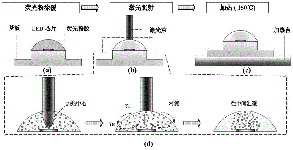
图1是本发明实施例一的封装过程示意图(实施例一采用不易固化的封装胶且荧光粉往中间汇聚的作用形式),其中(a)、(b)、(c)依次进行,(d)是(b)的详细过程。1 is a schematic diagram of the encapsulation process of the first embodiment of the present invention (the first embodiment adopts the encapsulation adhesive that is not easy to cure and the phosphor powder converges in the middle), wherein (a), (b), (c) are performed in sequence, (d) ) is the detailed process of (b).
图2是本发明实施例一荧光粉汇聚过程中不同时间下的图(实施例一采用不易固化的封装胶且荧光粉往中间汇聚的作用形式)。FIG. 2 is a diagram at different times during the phosphor aggregation process according to Embodiment 1 of the present invention (Embodiment 1 uses an encapsulant that is not easy to cure and the phosphors converge toward the middle).
图3是本发明实施例一中荧光粉汇聚前后的荧光粉胶的截面对比图(实施例一采用不易固化的封装胶且荧光粉往中间汇聚的作用形式),其中(a)是汇聚前、(b)是汇聚后。3 is a cross-sectional comparison view of the phosphor glue before and after the phosphors converge in the first embodiment of the present invention (the first embodiment uses a non-curable encapsulant and the phosphors converge toward the middle), wherein (a) is before the convergence, (b) is after aggregation.
图4是本发明实施例一和正常涂覆荧光粉胶的色温曲线对比图(实施例一采用不易固化的封装胶且荧光粉往中间汇聚的作用形式),图中方形为正常涂覆、圆形为实施例一。FIG. 4 is a comparison diagram of the color temperature curve between the first embodiment of the present invention and the normal coating of fluorescent powder glue (the first embodiment uses the encapsulation glue that is not easy to cure and the fluorescent powder converges in the middle), the square in the figure is the normal coating, the circle The shape is the first embodiment.
图5是本发明实施例一和正常涂覆荧光粉胶的荧光粉对比用量表(实施例一采用不易固化的封装胶且荧光粉往中间汇聚的作用形式)。FIG. 5 is a comparison table of the phosphor powder according to the first embodiment of the present invention and the phosphor powder glue coated normally (the first embodiment uses the encapsulation glue that is not easy to cure and the phosphor powder converges in the middle).
图6是本发明实施例二的封装过程示意图(实施例二采用易固化的封装胶、照射位置的荧光粉胶固化、未固化区域的荧光粉完全沉淀形成空间荧光粉图形的作用形式,即选择性固化的作用形式)。6 is a schematic diagram of the encapsulation process of the second embodiment of the present invention (in the second embodiment, an easily curable encapsulant, the phosphor glue in the irradiation position is cured, and the phosphor in the uncured area is completely precipitated to form a spatial phosphor pattern. form of action of sexual curing).
图7是本发明实施例二、正常涂覆荧光粉胶后使其自然静置至完全沉淀和正常涂覆荧光粉胶的色温曲线对比图(实施例二采用易固化的封装胶、照射位置的荧光粉胶固化、未固化区域的荧光粉完全沉淀形成空间荧光粉图形的作用形式,即选择性固化的作用形式),图中方形为实施例二、三角形为正常涂覆、圆形为正常涂覆荧光粉胶后使其自然静置至完全沉淀。7 is a comparison diagram of the color temperature curve of Embodiment 2 of the present invention, after normal coating of fluorescent powder glue and allowing it to stand until complete precipitation and normal coating of fluorescent powder glue The phosphor glue is cured and the phosphor in the uncured area is completely precipitated to form the action form of the spatial phosphor pattern, that is, the action form of selective curing), the square in the figure is Example 2, the triangle is normal coating, and the circle is normal coating After coating with fluorescent powder glue, let it stand naturally until it completely settles.
具体实施方式Detailed ways
下面结合附图和实施例对本发明作进一步的说明。The present invention will be further described below with reference to the accompanying drawings and embodiments.
实施例1Example 1
如图1所示,一种实现高空间颜色均匀性的LED封装方法,通过激光与荧光粉胶的作用控制荧光粉空间分布,包括步骤:先将LED芯片键合在基板上凹槽的中心位置并完成引线键合工艺,实现电连接;然后将荧光粉和封装胶充分混合成荧光粉胶后涂覆在LED芯片周围形成荧光粉层,荧光粉层被限制在凹槽区域内(如图1至图3所示,由于表面张力的作用,荧光粉层的形貌为球帽形);然后用激光照射荧光粉层,激光垂直指向LED芯片的中间,采用的是不易固化的封装胶,激光使荧光粉层中间温度高、边缘温度低,封装胶向中间流动,荧光粉在封装胶的裹挟下汇聚在中间LED芯片处;最后,对荧光粉胶进行加热固化(通过烘烤箱烘烤加热,加热温度150℃、加热时间1小时)。该方法用激光改善荧光粉分布,能够改善荧光粉层的几何形状,从而改善空间颜色均匀性,如图4所示,实现了高空间颜色均匀性,如图2和图3所示,能把周围无用的荧光粉汇聚到中间进行利用,如图5所示,节省了荧光粉的用量,从而降低封装成本。As shown in Figure 1, an LED packaging method to achieve high spatial color uniformity controls the spatial distribution of phosphors through the action of laser and phosphor glue, including the steps of: first bonding the LED chip to the center of the groove on the substrate And complete the wire bonding process to realize electrical connection; then fully mix the phosphor powder and the encapsulation glue to form a phosphor powder glue and coat it around the LED chip to form a phosphor powder layer, and the phosphor powder layer is limited in the groove area (as shown in Figure 1). As shown in Figure 3, due to the effect of surface tension, the morphology of the phosphor layer is spherical cap shape); then the phosphor layer is irradiated with a laser, and the laser is directed vertically to the middle of the LED chip. The middle temperature of the phosphor layer is high, and the edge temperature is low, the encapsulation glue flows to the middle, and the phosphor is gathered at the middle LED chip under the encapsulation glue; finally, the phosphor glue is heated and cured (by baking oven heating , heating temperature 150 ℃, heating time 1 hour). This method uses laser to improve the phosphor distribution, which can improve the geometry of the phosphor layer, thereby improving the spatial color uniformity. As shown in Figure 4, high spatial color uniformity is achieved. As shown in Figures 2 and 3, it can The useless phosphors around are gathered in the middle for utilization, as shown in FIG. 5 , which saves the amount of phosphors and reduces the packaging cost.
在实施例一中,激光功率为10w左右、照射时间为40s左右。In the first embodiment, the laser power is about 10w, and the irradiation time is about 40s.
实施例2Example 2
如图6所示,一种实现高空间颜色均匀性的LED封装方法,通过激光与荧光粉胶的作用控制荧光粉空间分布,包括步骤:先将LED芯片键合在基板上凹槽的中心位置并完成引线键合工艺,实现电连接;然后将荧光粉和封装胶充分混合成荧光粉胶后涂覆在LED芯片周围形成荧光粉层,荧光粉层被限制在凹槽区域内(如图1至图3所示,由于表面张力的作用,荧光粉层的形貌为球帽形);然后用激光照射荧光粉层,激光垂直指向LED芯片的中间,采用的是易固化的封装胶,激光使照射位置的荧光粉胶固化,再自然静置使未固化区域的荧光粉完全沉淀,形成空间荧光粉图形;最后,对荧光粉胶进行加热固化(通过烘烤箱烘烤加热,加热温度150℃、加热时间1小时)。该方法用激光改善荧光粉分布,能够改善荧光粉层的几何形状,从而改善空间颜色均匀性,如图7所示,实现高空间颜色均匀性。As shown in Figure 6, an LED packaging method to achieve high spatial color uniformity controls the spatial distribution of phosphors through the action of laser and phosphor glue, including the steps of: first bonding the LED chip to the center of the groove on the substrate And complete the wire bonding process to realize electrical connection; then fully mix the phosphor powder and the encapsulation glue to form a phosphor powder glue and coat it around the LED chip to form a phosphor powder layer, and the phosphor powder layer is limited in the groove area (as shown in Figure 1). As shown in Figure 3, due to the effect of surface tension, the morphology of the phosphor layer is spherical cap shape); then the phosphor layer is irradiated with a laser, and the laser is directed vertically to the middle of the LED chip. The phosphor glue at the irradiation position is cured, and then left to stand naturally to completely precipitate the phosphor in the uncured area to form a spatial phosphor pattern; finally, heat and cure the phosphor glue (bake and heat through a baking oven, the heating temperature is 150 °C). °C, heating time 1 hour). In this method, laser light is used to improve the phosphor distribution, which can improve the geometry of the phosphor layer, thereby improving the spatial color uniformity, as shown in Figure 7, to achieve high spatial color uniformity.
在实施例二中,激光功率为15w左右、照射时间为10s左右,自然静置时间为6小时左右。In the second embodiment, the laser power is about 15w, the irradiation time is about 10s, and the natural rest time is about 6 hours.
在本发明中,荧光粉胶中荧光粉的浓度可以为0.01g/ml~2.0g/ml,在本实施例一和实施例二中,荧光粉胶中荧光粉的浓度为1.5g/ml、荧光粉胶量为1.2μl。In the present invention, the concentration of fluorescent powder in the fluorescent powder glue can be 0.01g/ml~2.0g/ml. The amount of phosphor gel was 1.2 μl.
在本发明中,荧光粉胶通过喷头喷涂或注射器滴涂的方式进行涂覆。In the present invention, the phosphor glue is applied by spraying with a nozzle or drop-coating with a syringe.
本发明对激光的波长及光斑形状没有特殊要求,激光可以是蓝光、红外光或其他波长的光,光斑形状可以是圆形、方形或其他几何形状。在本实施例中,光斑为圆形、直径为0.5mm、波长为440nm。The present invention has no special requirements on the wavelength of the laser and the shape of the spot, the laser can be blue light, infrared light or light of other wavelengths, and the shape of the spot can be a circle, a square or other geometric shapes. In this embodiment, the light spot is circular, with a diameter of 0.5 mm and a wavelength of 440 nm.
本发明对封装胶的材料没有特殊要求,封装胶可以是硅胶、环氧树脂、液态玻璃或其它透明封装胶。The present invention has no special requirements on the material of the encapsulant, and the encapsulant can be silica gel, epoxy resin, liquid glass or other transparent encapsulant.
本发明对荧光粉的材料没有特殊要求,荧光粉可以是YAG、TAG或其它的荧光粉。The present invention has no special requirements on the material of the fluorescent powder, and the fluorescent powder can be YAG, TAG or other fluorescent powders.
本发明对基板的材料没有特殊要求,基板可以是铜、铝等金属基板材料,也可以是硅、陶瓷和PCB板等非金属基板材料。The present invention has no special requirements on the material of the substrate, and the substrate can be metal substrate materials such as copper and aluminum, or non-metal substrate materials such as silicon, ceramics, and PCB boards.
本发明对基板表面反光层的材料没有特殊要求,基板表面反光层可以是银或其它的反光材料。The present invention has no special requirements on the material of the reflective layer on the surface of the substrate, and the reflective layer on the surface of the substrate can be silver or other reflective materials.
本发明对LED芯片没有特殊要求,LED芯片可以是GaN等二元材料组成的芯片、AlGaNP等四元材料组成的芯片或其它芯片。The present invention has no special requirements on the LED chip, and the LED chip can be a chip composed of binary materials such as GaN, a chip composed of quaternary materials such as AlGaNP, or other chips.
以上所述为本发明的较佳实施例而已,但本发明不应该局限于该实施例和附图所公开的内容。所以凡是不脱离本发明所公开的精神下完成的等效或修改,都落入本发明保护的范围。The above description is only the preferred embodiment of the present invention, but the present invention should not be limited to the content disclosed in the embodiment and the accompanying drawings. Therefore, all equivalents or modifications accomplished without departing from the disclosed spirit of the present invention fall into the protection scope of the present invention.
Claims (10)
Priority Applications (1)
| Application Number | Priority Date | Filing Date | Title |
|---|---|---|---|
| CN201910644219.8A CN110429167B (en) | 2019-07-17 | 2019-07-17 | LED packaging method to achieve high spatial color uniformity |
Applications Claiming Priority (1)
| Application Number | Priority Date | Filing Date | Title |
|---|---|---|---|
| CN201910644219.8A CN110429167B (en) | 2019-07-17 | 2019-07-17 | LED packaging method to achieve high spatial color uniformity |
Publications (2)
| Publication Number | Publication Date |
|---|---|
| CN110429167A CN110429167A (en) | 2019-11-08 |
| CN110429167B true CN110429167B (en) | 2020-12-08 |
Family
ID=68409802
Family Applications (1)
| Application Number | Title | Priority Date | Filing Date |
|---|---|---|---|
| CN201910644219.8A Expired - Fee Related CN110429167B (en) | 2019-07-17 | 2019-07-17 | LED packaging method to achieve high spatial color uniformity |
Country Status (1)
| Country | Link |
|---|---|
| CN (1) | CN110429167B (en) |
Families Citing this family (1)
| Publication number | Priority date | Publication date | Assignee | Title |
|---|---|---|---|---|
| CN114535024A (en) * | 2022-03-28 | 2022-05-27 | 广东工业大学 | LED fluorescent powder glue dispensing method based on continuous laser |
Citations (1)
| Publication number | Priority date | Publication date | Assignee | Title |
|---|---|---|---|---|
| CN101553936A (en) * | 2006-05-31 | 2009-10-07 | 飞利浦拉米尔德斯照明设备有限责任公司 | Color control by changing wavelength converting member |
Family Cites Families (9)
| Publication number | Priority date | Publication date | Assignee | Title |
|---|---|---|---|---|
| JPWO2014119295A1 (en) * | 2013-01-31 | 2017-01-26 | パナソニックIpマネジメント株式会社 | Method for manufacturing light emitting device |
| US9698314B2 (en) * | 2013-03-15 | 2017-07-04 | General Electric Company | Color stable red-emitting phosphors |
| CN103681983B (en) * | 2013-06-17 | 2016-02-24 | 深圳市绎立锐光科技开发有限公司 | A kind of light-emitting component applies method and the air jet system of phosphor powder layer |
| CN103325926B (en) * | 2013-06-19 | 2015-07-22 | 华中科技大学 | LED packaging structure used in on-board chip and fluorescent powder coating method thereof |
| CN104979452A (en) * | 2014-04-08 | 2015-10-14 | 刘胜 | Method for manufacturing and packaging light-emitting diode chip on wafer |
| CN104465965B (en) * | 2014-12-09 | 2018-06-19 | 武汉大学 | A kind of fluorescent powder film preparation method for white light LEDs wafer-level packaging |
| CN105070794B (en) * | 2015-07-14 | 2017-06-16 | 武汉大学 | LED fluorescent powder coating unit and method based on induced with laser |
| KR20170093320A (en) * | 2016-02-04 | 2017-08-16 | 주식회사 효성 | Phosphor plate with light-diffusing material |
| DE102016212070A1 (en) * | 2016-07-04 | 2018-01-04 | Osram Gmbh | LIGHTING DEVICE AND VEHICLE HEADLIGHTS WITH LIGHTING DEVICE |
-
2019
- 2019-07-17 CN CN201910644219.8A patent/CN110429167B/en not_active Expired - Fee Related
Patent Citations (1)
| Publication number | Priority date | Publication date | Assignee | Title |
|---|---|---|---|---|
| CN101553936A (en) * | 2006-05-31 | 2009-10-07 | 飞利浦拉米尔德斯照明设备有限责任公司 | Color control by changing wavelength converting member |
Non-Patent Citations (1)
| Title |
|---|
| 彩色PDP荧光粉的发展现状与制备方法;尚淑娟等;《稀土》;20100615(第03期);全文 * |
Also Published As
| Publication number | Publication date |
|---|---|
| CN110429167A (en) | 2019-11-08 |
Similar Documents
| Publication | Publication Date | Title |
|---|---|---|
| CN101075655B (en) | White surface light source lighting device | |
| CN104393154A (en) | Wafer level packaging method for LED (Light-Emitting Diode) chip level white light source | |
| CN201039523Y (en) | A high-power white LED device with high color rendering index | |
| CN106531857A (en) | Chip scale LED packaging structure and packaging technology | |
| CN103872034A (en) | Total-angle light emitting LED light source based on light transmission substrate and packaging method of total-angle light emitting LED light source | |
| CN203839375U (en) | Large-power LED chip integrated packaging structure | |
| CN102034919A (en) | High-brightness high-power light-emitting diode (LED) and manufacturing method thereof | |
| CN103928450B (en) | Product for packaging LEDs with uniform light color and manufacturing method of product | |
| CN104534421A (en) | LED light source module with highlight power density | |
| CN201708188U (en) | Ceramic high-power light emitting diode | |
| CN104953017A (en) | Integrated LED (light emitting diode) packaging piece based on inverted powder coating strap secondary light distribution reinforcement and production technology | |
| CN102569558A (en) | Packaging method for realizing separation of fluorescent powder glue away from coating in light emitting diode (LED) package and application | |
| CN110429167B (en) | LED packaging method to achieve high spatial color uniformity | |
| CN102637810A (en) | LED (light-emitting diode) packaging structure and packaging molding method | |
| CN104253199A (en) | A LED package structure and a manufacture method thereof | |
| US9752764B2 (en) | Wide-angle emitting LED driven by built-in power and assembly method thereof | |
| CN105449083A (en) | LED fluorescent powder glue coating method | |
| CN105575957A (en) | COB light source for white light LED | |
| CN206116449U (en) | White light LED wrapper spare | |
| CN101572287B (en) | A kind of active packaging method of white light LED based on blue light LED chip | |
| CN101030610B (en) | Large-power light-emitting diodes and its fluorescent-powder coating method | |
| CN107706289A (en) | Quantum dot LED and preparation method thereof | |
| CN103199184B (en) | A kind of encapsulating structure improving vertical LED chip brightness | |
| CN102280555A (en) | Light-emitting diode and manufacturing method thereof | |
| CN201829498U (en) | Light emitting diode (LED) integrated light source panel |
Legal Events
| Date | Code | Title | Description |
|---|---|---|---|
| PB01 | Publication | ||
| PB01 | Publication | ||
| SE01 | Entry into force of request for substantive examination | ||
| SE01 | Entry into force of request for substantive examination | ||
| GR01 | Patent grant | ||
| GR01 | Patent grant | ||
| CF01 | Termination of patent right due to non-payment of annual fee |
Granted publication date: 20201208 Termination date: 20210717 |
|
| CF01 | Termination of patent right due to non-payment of annual fee |