This application claims priority to U.S. provisional patent application No.62/395,505, filed on 2016, 9, 16, the entire disclosure of which is hereby incorporated by reference.
Detailed Description
Fig. 1 is a simplified block diagram of a load control device (e.g., a Light Emitting Diode (LED) driver 100) for controlling the amount of power delivered to an electrical load, such as an LED light source 102 (e.g., an LED light engine), and thus controlling the intensity of the electrical load. Depending on the particular lighting system, the LED light source 102 is shown as a plurality of LEDs connected in series but may comprise a single LED or a plurality of LEDs connected in parallel or a suitable combination thereof. The LED light source 102 may include one or more Organic Light Emitting Diodes (OLEDs). The light source 102 may include one or more quantum dot light emitting diodes (QLEDs). LED driver 100 may include a hot terminal H and a neutral terminal. These terminals may be adapted to be coupled to an Alternating Current (AC) power source (not shown).
LED driver 100 may include a Radio Frequency Interference (RFI) filter circuit 110, a rectifier circuit 120, a boost converter 130, a load regulation circuit 140, a control circuit 150, a current sensing circuit 160, a memory 170, a communication circuit 180, and/or a power supply 190. The RFI filter circuit 110 may minimize noise provided on the AC mains. Rectifier circuit 120 can generate a rectified voltage VRECT。
The
boost converter 130 may receive the rectified voltage V
RECTAnd across the bus capacitor C
BUSGenerating a boosted Direct Current (DC) bus voltage V
BUS. Boost converter 130 may include any suitable power converter circuitry for generating an appropriate bus voltage, such as, for example, a flyback converter, a single-ended primary inductor converter (SEPIC), a flyback converter, a flyback converter, a flyback converter, a flyback converter, a flyback converter, a flyback converter, a converter,
a converter or other suitable power converter circuit.
Boost converter 120 may operate as a Power Factor Correction (PFC) circuit to adjust the power factor of
LED driver 100 towards power factor one.
The load regulation circuit 140 may receive the bus voltage VBUSAnd controlling the amount of power delivered to the LED light source 102, e.g., to a low-end (e.g., minimum) intensity LLE(e.g., about 1-5%) and high-end (e.g., maximum) intensity LHE(e.g., about 100%) of the LED light sources 102. An example of the load regulation circuit 140 may be an isolated half-bridge forward converter. An example of a LOAD CONTROL DEVICE (e.g., LED driver 100) including a forward converter is described in more detail in commonly assigned U.S. patent application No.13/935,799 entitled "LOAD CONTROL DEVICE FOR LIGHT EMITTING DIODE LIGHT SOURCE" filed on 5.7.2013, the entire disclosure of which is hereby incorporated by reference. The load regulation circuit 140 may include, for example, a buck converter, a linear regulator, or any suitable LED drive circuit for adjusting the intensity of the LED light source 102.
The control circuit 150 may be configured to control the operation of the boost converter 130 and/or the load regulation circuit 140. An example of the control circuit 150 may be a controller. The control circuit 150 may comprise, for example, a digital controller or any other suitable processing device, such as, for example, a microcontroller, a Programmable Logic Device (PLD), a microprocessor, an Application Specific Integrated Circuit (ASIC), or a Field Programmable Gate Array (FPGA). The control circuit 150 can generate bus line electricityVoltage control signal VBUS-CNTLWhich may be provided to the boost converter 130 for adjusting the bus voltage VBUSOf the amplitude of (c). The control circuit 150 may receive the bus voltage feedback control signal V from the boost converter 130BUS-FBWhich can indicate the bus voltage VBUSOf the amplitude of (c).
The control circuit 150 may generate the driving control signal VDRIVE1、VDRIVE2. Can drive the control signal VDRIVE1、VDRIVE2Is provided to the load regulation circuit 140 for adjusting the load voltage V generated across the LED light source 102LOADAnd/or the load current I conducted through the LED light source 120LOADOf the amplitude of (c). By controlling the load voltage VLOADAnd/or the load current ILOADThe control circuit may control the intensity of the LED light source 120 to the target intensity LTRGT. The control circuit 150 can adjust the driving control signal VDRIVE1、VDRIVE2Of operating frequency fOPAnd/or duty cycle DCINV(e.g., on-time T)ON) In order to adjust the load voltage VLOADAnd/or the load current ILOADOf the amplitude of (c).
The current sensing circuit 160 may receive a sensing voltage VSENSE. Sensing voltage VSENSEMay be generated by the load regulation circuit 140. Sensing voltage VSENSECan indicate the load current ILOADOf the amplitude of (c). Current sensing circuit 160 may receive signal chopper control signal V from control circuit 150CHOP. The current sensing circuit 160 may generate a load current feedback signal VI-LOADIt may be an indication of the load current ILOADAverage amplitude of (I)AVEThe DC voltage of (1). The control circuit 150 may receive a load current feedback signal V from the current sensing circuit 160I-LOAD. The control circuit 150 may be based on the load current feedback signal VI-LOADAdjusting a drive control signal VDRIVE1、VDRIVE2So that the target load current I can be directedTRGTRegulating the load current ILOADOf the amplitude of (c). For example, the control circuit 150 may be arranged to drive the control signal VDRIVE1、VDRIVE2Initial operation ofParameter (e.g. operating frequency f)OPAnd/or duty cycle DCINV). The control circuit 150 may receive an indication driving control signal VDRIVE1、VDRIVE2Of the load current feedback signal VI-LOAD. Based on the indication, the control circuit 150 may adjust an operating parameter of the drive control signal to thereby drive the target load current I towardsTRGTRegulating the load current ILOADE.g., using a control loop).
Load current ILOADMay be a current conducted through the LED light source 102. Target load current ITRGTIt may be the current that the control circuit 150 is intended to conduct through the LED light source 102 (e.g., based at least on the load current feedback signal V)I-LOAD). Load current ILOADCan be approximately equal to the target load current ITRGTBut may not always follow the target load current ITRGT. This may be because, for example, the control circuit 150 may have a particular level of granularity at which it may control the current conducted through the LED light source 102 (e.g., due to inverter cycle length, etc.). Non-ideal response (e.g., load current I) of LED light source 102LOADOvershoot in) can also cause the load current ILOADOff-target load current ITRGT. Those skilled in the art will appreciate that the graphs shown herein (e.g., fig. 2 and 13) illustrating the current conducted through the LED light source as a linear graph illustrate the target load current ITRGTDue to the load current ILOADIt may not actually follow a true linear path by itself.
The control circuit 150 may be coupled to a memory 170. The memory 170 may store an operating characteristic (e.g., target intensity L) of the LED driver 100TRGTLow end intensity LLEHigh end strength LHEEtc.). The communication circuit 180 may be coupled to, for example, a wired communication link or a wireless communication link, such as a Radio Frequency (RF) communication link or an Infrared (IR) communication link. The control circuit 150 may be configured to update the target intensity L of the LED light source 102 in response to a digital message received via the communication circuit 180TRGTAnd/or operating characteristics stored in the memory 170. The LED driver 100 may be operableTo receive a phase control signal from the dimmer switch for determining a target intensity L for the LED light source 102TRGT. The power supply 190 may receive a rectified voltage VRECTAnd generates a Direct Current (DC) supply voltage VCCFor powering the circuitry of the LED driver 100.
FIG. 2 is a graph showing the intensity L according to the targetTRGTTarget load current I ofTRGTExample graph of (a). As shown, at target intensity LTRGTAnd a target load current ITRGTThere may be a linear relationship between (e.g., in at least an ideal case). For example, to achieve a higher target intensity, the control circuit 150 may increase the target load current ITRGT(e.g., proportional to an increase in target intensity); to achieve a lower target intensity, the control circuit 150 may reduce the target load current ITRGT(e.g., in proportion to a decrease in target intensity). With target load current ITRGTIs being regulated, the load current ILOADMay be changed accordingly. However, a load current I may be presentLOADLimits of how much can be adjusted. For example, the load current I may not be reducedLOADAdjusted to be higher than the maximum rated current IMAXOr below the minimum rated current IMIN(e.g., due to hardware limitations of the load regulation circuit 140 and/or the control circuit 150). Thus, the control circuit 150 may be configured to operate at the minimum rated current IMINWith maximum rated current IMAXTo adjust the target load current ITRGTSo that the load current ILOADMay fall within the same range. Maximum rated current IMAXMay correspond to a high end intensity LHE(e.g., about 100%). Minimum rated current IMINMay correspond to the transition intensity LTRAN(e.g., about 5%). At high end intensity LHEAnd transition strength LTRANMeanwhile, the control circuit 150 may operate the load adjusting circuit 140 in a normal mode in which the load current I may be adjustedLOADAverage amplitude of (I)AVEIs controlled to be equal (e.g., approximately equal) to the target load current ITRGT. For example, during the normal mode, the control circuit 150 mayResponsive to a load current feedback signal VI-LOAD(e.g. using closed loop control) to control the load current ILOADAverage amplitude of (I)AVEControlled to a target load current ITRGT。
To supply a load current ILOADAverage amplitude of (I)AVEAdjusted to be lower than the minimum rated current IMIN(and thus the target intensity LTRGTAdjusted to be lower than the transition strength LTRAN) The control circuit 150 may be configured to operate the load regulation circuit 140 in a burst mode. The burst mode may be characterized by a burst operation period comprising an active state period and an inactive state period. During the active state periods, the control circuit 150 may be configured to regulate the load current I in a manner similar to those in the normal modeLOAD. During periods of inactivity, the control circuit 150 may be configured to stop regulating the load current ILOAD(e.g., to allow load current ILOADDown to about zero). Ratio of active state period to burst operation period (e.g., T)ACTIVE/TBURST) Can represent burst duty cycle DCBURST. Can be at the maximum duty cycle DCMAX(e.g., about 100%) and minimum duty cycle DCMIN(e.g., about 20%) between control burst duty cycle DCBURST. Can be directed towards the target current I during the active state period of the burst modeTRGT(e.g., minimum rated current I)MIN) Regulating the load current ILOAD. Duty cycle of burst DCBURSTSet to less than maximum duty cycle DCMAXCan be set to the load current ILOADAverage amplitude of (I)AVEDown to less than the minimum rated current IMIN。
FIG. 3 is a graph showing the intensity L according to the targetTRGTBurst duty cycle of DCBURST(e.g., ideal burst duty cycle DC)BURST-IDEAL) Example graph of (a). As described herein, when the target intensity LTRGTAt high end intensity LHE(e.g., about 100%) and transition strength LTRAN(e.g., about 5%), the control circuit 150 may be configured to operate the load regulation circuit 1 in the normal mode40, e.g. by duty cycling the bursts DCBURSTSet at or about maximum duty cycle DCMAXOr a constant value of about 100%. In order to adjust the target intensity LTRGTAdjusted to be lower than the transition strength LTRANThe control circuit 150 may be configured to operate the load regulation circuit 140 in burst mode, e.g., by DC at maximum duty cycleMAXWith minimum duty cycle DCMIN(e.g., about 20%) to adjust the burst duty cycle DCBURST。
Referring to fig. 3, burst duty cycle DCBURSTCan refer to ideal burst duty cycle DCBURST-IDEALWhich may include an integer part DCBURST-INTEGERAnd/or fractional partial DCBURST-FRACTIONAL. Integer part DCBURST-INTEGERThe desired burst duty cycle DC may be determined by a desired burst duty cycle including a complete inverter cycle (e.g., an integer value of an inverter cycle)BURST-IDEALIs characterized by the percentage of (c). Fractional part DCBURST-FRACTIONALCan be controlled by an ideal burst duty cycle DC that includes a fraction of the inverter cycleBURST-IDEALIs characterized by the percentage of (c). In at least some cases, the control circuit 150 (e.g., via the load regulation circuit 140) may be configured to adjust the number of inverter cycles by an integer number (e.g., DC)BURST-INTEGER) Rather than a fractional amount (e.g., DC)BURST-FRACTIONAL). Thus, although the example graph illustration of FIG. 3 shows an ideal burst duty cycle DCBURST-IDEALFrom maximum duty cycle DCMAXTo minimum duty cycle DCMINHowever, unless otherwise defined, the burst duty cycle DCBURSTCan refer to ideal burst duty cycle DCBURST-IDEALInteger part of (D)BURST-INTEGER(e.g., if the control circuit 150 is not configured to operate the burst duty cycle DC at a fractional amountBURST)。
Fig. 4 is an example state diagram illustrating operation of load regulation circuit 140 in burst mode. During burst mode, the control circuit 150 may, for example, DC according to a burst duty cycleBURSTAnd a burst mode period TBURST(e.g., about 4.4 milliseconds) periodically controlling the load regulation circuit 140Into an active state and an inactive state. For example, active state period TACTIVEMay be equal to the burst duty cycle DCBURSTBy the burst mode period TBURSTAnd a period of inactive state TINACTIVEMay be equal to one minus the burst duty cycle DCBURSTBy the burst mode period TBURST. That is, TACTIVE=DCBURST·TBURSTAnd TINACTIVE=(1-DCBURST)·TBURST。
In the active state of the burst mode, the control circuit 150 may be configured to generate the driving control signal VDRIVE1、VDRIVE2. The control circuit 150 may also be configured to adjust the drive control signal VDRIVE1、VDRIVE2Of operating frequency fOPAnd/or duty cycle DCINV(e.g., on-time T)ON) To adjust the load current ILOADOf the amplitude of (c). The control circuit 150 may be configured to make adjustments using closed loop control. For example, in the active state of the burst mode, the control circuit 150 may generate the driving signal VDRIVE1、VDRIVE2In response to a load current feedback signal VI-LOADTo apply a load current ILOADIs adjusted to be equal to the target load current ITRGT(e.g., minimum rated current I)MIN)。
In the inactive state of the burst mode, the control circuit 150 can let the load current ILOADIs reduced to about zero amperes, e.g. by freezing the closed-loop control and/or not generating the drive control signal VDRIVE1、VDRIVE2. While the control loop is frozen (e.g., in an inactive state), the control circuit 150 may stop feeding the signal V back to the load currentI-LOADIn response (e.g., the control circuit 150 may not adjust the operating frequency f in response to the load current feedback signalOPAnd/or duty cycle DCINVValue of (d). The control circuit 150 may drive the control signal V before (e.g., immediately before) freezing the control loopDRIVE1、VDRIVE2Current duty cycle of DCINV(e.g., current on-time TON) Storage existenceIn reservoir 170. When the control loop is thawed (e.g., when the control circuit 150 enters the active state), the control circuit 150 may resume using the operating frequency f from the previous active stateOPAnd/or duty cycle DCINVTo generate a driving control signal VDRIVE1、VDRIVE2。
The control circuit 150 may be configured to adjust the burst duty cycle DC using open loop controlBURST. For example, the control circuit 150 may be configured to determine when the target intensity L is less than the target intensityTRGTLower than the transition strength LTRANAccording to the target intensity LTRGTTo adjust burst duty cycle DCBURST. For example, the control circuit 150 may be configured to follow the target intensity LTRGTIs reduced to below the transition intensity LTRAN(e.g., as shown in FIG. 3) to linearly reduce the burst duty cycle DCBURSTHowever, target load current ITRGTAt a minimum rated current IMINRemains constant (e.g., as shown in fig. 2). Since the control circuit 150 may be DC in accordance with the burst duty cycleBURSTAnd a burst mode period TBURSTSwitching between an active state and an inactive state (e.g., as shown in the state diagram of fig. 4), so the load current ILOADAverage amplitude of (I)AVECan be based on burst duty cycle DCBURSTTo change (e.g. I)AVE=DCBURST·TMIN). In other words, during burst mode, the load current ILOADPeak amplitude of (I)PKCan be equal to the minimum rated current IMINBut depends on the burst duty cycle DCBURSTValue of (1), load current ILOADAverage amplitude of (I)AVECan be less than the minimum rated current IMIN。
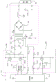
Fig. 5 is a simplified schematic diagram of forward converter 240 and current sensing circuit 260 of an LED driver (e.g., LED driver 100 shown in fig. 1). The forward converter 240 may be an example of the load regulation circuit 140 of the LED driver 100 shown in fig. 1. The current sensing circuit 260 may be an example of the current sensing circuit 160 of the LED driver 100 shown in fig. 1.
Forward converter 240 may include a transistor having two field effect transistorsTubes (FET) Q210, Q212 for example from bus voltage VBUSGenerating a high-frequency inverter voltage VINVThe half-bridge inverter circuit of (1). Can respond to the driving control signal VDRIVE1、VDRIVE2Causing FETs Q210, Q212 to be conductive and non-conductive. Can receive the driving control signal V from the control circuit 150DRIVE1、VDRIVE2. Drive control signal VDRIVE1、VDRIVE2May be coupled to the gates of the respective FETs Q210, Q212 via a gate drive circuit 214 (which may include, for example, part number L6382DTR manufactured by ST Microelectronics). The control circuit 150 may be configured to operate at a frequency fOP(e.g., about 60-65kHz) to generate the inverter voltage VINVAnd thus produces an operating period TOP. The control circuit 150 may be configured to adjust the operating frequency f under certain operating conditionsOP. For example, the control circuit 150 may be configured to reduce the high-end intensity LHEThe nearby operating frequency. The control circuit 150 may be configured to adjust the inverter voltage VINVDuty cycle of DCINV(e.g., with or without likewise adjusting the operating frequency) to face the target intensity LTRGTControlling the intensity of the LED light source 202.
In the normal mode of operation, when the target intensity L of the LED light source 202 isTRGTAt high end intensity LHEAnd transition strength LTRANIn between, the control circuit 150 may adjust the inverter voltage VINVDuty cycle of DCINVTo face a target load current ITRGTRegulating the load current ILOADAmplitude (e.g., average amplitude I)AVE). Load current ILOADCan be at the maximum rated current IMAXWith minimum rated current IMINFor example, as shown in fig. 2. Minimum on-time T of half-bridge inverter circuit which may be based on forward converter 240, for exampleON-MINDetermination of the minimum rated current IMIN. Minimum on-time TON-MINMay vary based on the hardware limitations of the forward converter. At a minimum rated current IMINLower (e.g., at transition intensity L)TRANLower), the inverter voltage VINVThe frequency f can be operated by a low endOP-LEAnd a low end operating period TOP-LETo characterize.
When the target intensity L of the LED light source 202 isTRGTLower than the transition strength LTRANWhen desired, the control circuit 150 may be configured to operate the forward converter 240 in a burst mode of operation. In addition to or instead of using the target intensity as a threshold for determining when to operate in burst mode, the control circuit 150 may use power (e.g., transition power) and/or current (e.g., transition current) as thresholds. In a burst mode of operation, the control circuit 150 may be configured to be in an active state (e.g., in which the control circuit 150 may actively generate the drive control signal VDRIVE1、VDRIVE2To reduce the load current ILOADPeak amplitude of (I)PKRegulated to equal minimum rated current IMIN) And an inactive state (e.g., where the control circuit 150 freezes the control loop and does not generate the drive control signal V)DRIVE1、VDRIVE2) To switch the forward converter 240. Fig. 4 shows a state diagram illustrating the transition between two states. The control circuit 150 may be DC according to a burst duty cycleBURSTAnd/or a burst mode period TBURSTThe forward converter 240 is switched between an active state and an inactive state (e.g., as shown in fig. 4). The control circuit 150 may be configured to control the current level of the current source based on the magnitude of the current that may be below the transition level LTRANTarget intensity L ofTRGTTo adjust burst duty cycle DCBURST(e.g., as shown in fig. 3). In the active state of the burst mode (and in the normal mode), the forward converter 240 may be turned on for a time TTURN-ONAnd closing time TTURN-OFFTo characterize. On-time TTURN-ONMay be a slave drive control signal VDRIVE1、VDRIVE2A period of time when driven until the respective FET Q210, Q212 is rendered conductive. Off time TTURN-OFFMay be a slave drive control signal VDRIVE1、VDRIVE2Is driven until the respective FET Q210, Q212 is rendered non-conductive.
Inverter voltage VINVMay be coupled to the primary winding of transformer 220 by a dc blocking capacitor C216 (which may have a capacitance of about 0.047 muf, for example). The primary voltage V can be generated across the primary windingPRI. The transformer 220 may be constructed with a turns ratio n that may be about 115:29TURNS(e.g., N)1/N2) To characterize. A sense voltage V may be generated across sense resistor R222SENSEThe sense resistor R222 may be coupled in series with the primary winding of the transformer 220. The FETs Q210, Q212 and the primary winding of transformer 220 may each be formed by a parasitic capacitance CP1、CP2、CP3To characterize. The secondary winding of the transformer 220 may generate a secondary voltage. The secondary voltage may be coupled to the AC terminals of a full wave diode rectifier bridge 224 for rectifying the secondary voltage generated across the secondary winding. The positive DC terminal of the rectifier bridge 224 may be coupled to the LED light source 202 through an output energy storage inductor L226 (which may have an inductance of about 10mH, for example). The load voltage V may be generated across an output capacitor C228 (e.g., which may have a capacitance of about 3 μ F)LOAD。
The current sensing circuit 260 may include circuitry for generating a load current feedback signal VI-LOADThe averaging circuit of (1). The averaging circuit may comprise a low pass filter. The low pass filter may include a capacitor C230 (which may have a capacitance of about 0.066 μ F, for example) and a resistor R232 (which may have a resistance of about 3.32k Ω, for example). The low pass filter may receive the sensing voltage V via a resistor R234 (e.g., which may have a resistance of about 1k Ω)SENSE. The current sensing circuit 160 may include a transistor Q236 (e.g., a FET as shown in fig. 5). Transistor Q236 may be coupled between the junction of resistors R232, R234 and circuit common. The gate of transistor Q236 may be coupled to circuit common through a resistor R238 (which may have a resistance of about 22k Ω, for example). The gate of transistor Q236 may receive a signal-chopper control signal V from control circuit 150CHOP. Entitled "Forward CONVERTER with Primary side Current sensing Circuit" (FORWARD CONVERTER HAVING A PRIMARY-An example of CURRENT sensing CIRCUIT 260 is described in more detail in commonly assigned U.S. patent application No.13/834,153 to SIDE CURRENT SENSE CIRCUIT), the entire disclosure of which is incorporated herein by reference.
Fig. 6 is a diagram illustrating an example set of magnetic cores 290 of an energy storage inductor (e.g., output energy storage inductor L226 of forward converter 240 shown in fig. 5). The magnetic core set 290 may include two E-cores 292A, 292B and may include part number PC40EE16-Z manufactured by TDK corporation. The E-cores 292A, 292B may include respective outer legs 294A, 294B and inner legs 296A, 296B. The inner legs 296A, 296B may have a width wLEG(e.g., about 4 mm). The inner leg 296A of the first E-core 292A may include a partial gap 298A (e.g., the magnetic core set 290 may be partially gapped) such that the inner legs 296A, 296B may be spaced apart by a gap distance dGAP(e.g., about 0.5 mm). The partial gap 298A may extend for a gap width wGAP(e.g., about 2.8mm) such that the partial gap 298A may extend up to the leg width w of the inner leg 296ALEGAbout 70% of the total. Either or both of the inner legs 296A, 296B may include a partial gap. The partially gapped core set 290 (e.g., as shown in fig. 6) may allow the output energy storage inductor L226 of the forward converter 240 (e.g., as shown in fig. 5) to operate under low load conditions (e.g., at the low-end intensity L)LENearby) to maintain a continuous current.
Fig. 7 shows waveforms illustrating example operations of a forward converter (e.g., forward converter 240) and a current sensing circuit (e.g., current sensing circuit 260). For example, when operating in normal mode and in the active state of burst mode as described herein, forward converter 240 may generate the waveforms shown in fig. 7. As shown in fig. 7, a control circuit (e.g., control circuit 150) may provide a corresponding drive control signal VDRIVE1、VDRIVE2Driven up to about supply voltage VCCTo render the respective FETs Q210, Q212 conductive for an on-time TON. The FETs Q210, Q212 may be rendered conductive at different times. When the high-side FET Q210 is on, the primary winding of the transformer 220 may be, for example, by a capacitorThe primary current I is converted by the C216 and the sense resistor R222PRITo the circuit common. After (e.g., immediately after) the high-side FET Q210 is rendered conductive (at time t in FIG. 7)1) E.g. due to parasitic capacitance C of the transformer 220 as shown in fig. 7P3Primary current IPRIShort high amplitude pulses can be exhibited. While the high-side FET Q210 is conducting, the capacitor C216 may charge so that the bus voltage V may develop across the capacitorBUSIs about half the magnitude of (a). Primary voltage V across the primary winding of transformer 220PRIMay be equal to the bus voltage VBUSAbout half the amplitude of (e.g., V)BUS/2). When the low-side FET Q212 is on, the primary winding of the transformer 220 may conduct the primary current I in the opposite directionPRIAnd a capacitor C216 may be coupled across the primary winding such that the primary voltage VPRIMay have a magnitude equal to the bus voltage VBUSA negative polarity of about half the amplitude.
When either of the high-side FET Q210 and the low-side FET Q212 is on, the output inductor current I conducted by the output inductor L226LAnd/or a load voltage V across the LED light source 202LOADMay increase with respect to time. While the FETs Q210, Q212 are on (e.g., after an initial current spike), the primary current IPRIMay increase with respect to time. When the FETs Q210, Q212 are non-conductive, the inductor current I is outputLAnd a load voltage VLOADMay be reduced in amplitude with respect to time. Output inductor current ILCan be determined from the peak amplitude IL-PKAnd average amplitude IL-AVGFor example, as shown in fig. 7. The control circuit 150 may increase and/or decrease the drive control signal VDRIVE1、VDRIVE2On-time T ofON(e.g., and inverter voltage VINVDuty cycle of DCINV) To increase and/or decrease, respectively, the output inductor current ILAverage amplitude of (I)L-AVGAnd thus respectively increase and/or decrease the intensity of LED light source 202.
When FET Q210When Q212 is rendered non-conductive, the primary current IPRIMay be reduced towards zero amps (e.g., as shown in fig. 7 at time t2 when the high-side FET Q210 is rendered non-conductive). For example, due to the magnetizing inductance L of the transformerMAGMagnetization current IMAGMay continue to flow through the primary winding of transformer 220. When the target intensity L of the LED light source 102TRGTAt the low end intensity LLENear time, primary current IPRIMay oscillate after any of the FETs Q210, Q212 are rendered non-conductive. The oscillation may be due to parasitic capacitance C of the FETP1、CP2Parasitic capacitance C of the primary winding of transformer 220P3And/or other parasitic capacitances of the circuit (e.g., such as parasitic capacitances of a printed circuit board on which the forward converter 240 is mounted).
Primary current IPRICan indicate the secondary current ISECAnd thus the intensity of the LED light source 202. Magnetizing current IMAG(e.g. primary current IPRIThe reactive component) may flow through the sense resistor R222. When the high-side FET Q210 is turned on, the magnetizing current IMAGCan be changed from negative to positive. When the low-side FET Q212 is turned on, the magnetizing current IMAGMay be changed from positive to negative polarity. When the primary voltage VPRIAt an amplitude of zero volts, the magnetizing current IMAGMay be held constant, for example, as shown in fig. 7. Magnetizing current IMAGMay have a maximum amplitude defined by the following equation:
wherein T isHCMay be the inverter voltage VINVA half cycle period of, e.g., THC=TOP/2. As shown in FIG. 7, the regions 250, 252 may be approximately equal, such that the magnetizing current IMAGIs at the initial voltage VPRIIs greater than about zero volts (e.g., during an on-time T as shown in fig. 7ONDuration) may be zero.
The current sensing circuit 260 may be at the inverter voltage VINVDetermines the primary current I (e.g., when the high-side FET Q210 is on)PRIAverage value of (a). As described herein, the high-side FET Q210 may be on for a time TONDuring which it is turned on. The current sensing circuit 260 may generate a load current feedback signal VI-LOADWhich may have as a primary current IPRIThe DC amplitude of the average value (e.g., when the high-side FET Q210 is on). Because of the magnetizing current IMAGDuring the period of time that the high-side FET Q210 is on (e.g., at the on-time T)ONPeriod) may be approximately zero, so the load current feedback signal V generated by the current sensing circuitI-LOADCan indicate the primary current IPRI(e.g., at on-time TONPeriod) of the real component (e.g., only the real component).
When the high-side FET Q210 is rendered conductive, the control circuit 150 can direct the signal-chopper control signal V toward circuit commonCHOPDriving Low to cause transistor Q236 of current sensing circuit 260 to not conduct for Signal chopper time TCHOP. Time T of signal chopperCHOPMay be approximately equal to the on-time T of the high-side FET Q210ONFor example, as shown in FIG. 7, capacitor C230 may be at the signal chopper control signal VCHOPIs low while sensing voltage V through resistors R232, R234SENSEAnd (6) charging. Load current feedback signal VI-LOADMay be the primary current IPRIAnd may indicate the real component of the primary current during the time when the high-side FET Q210 is non-conductive. When the high-side FET Q210 is non-conductive, the control circuit 150 can apply a signal chopper control signal VCHOPDriven high to render transistor Q236 conductive. Thus, as described herein, the control circuit 150 may be capable of feeding back the signal V as a function of the load currentI-LOADTo determine the load current ILOADAt least in part because the magnetizing current I can be reduced or eliminatedMAGAnd a primary current IPRIIs fed back to the load currentI-LOADThe amplitude of (c).
With target intensity L of LED light source 202TRGTIs directed towards the low end intensity LLEReducing and/or following the drive control signal VDRIVE1、VDRIVE2On-time T ofONBecoming smaller and smaller, the parasitic capacitance of the load regulation circuit 140 (e.g., parasitic capacitance C of FETs Q210, Q212)P1、CP2Parasitic capacitance C of the primary winding of transformer 220P3And/or other parasitic capacitances of the circuit) may cause the primary voltage V to bePRIIs slowly reduced towards zero volts after the FETs Q210, Q212 are rendered non-conductive.
FIG. 8 shows a graph illustrating the intensity L of the targetTRGTAt the low end intensity LLEExample waveforms of the operation of the forward converter and the current sensing circuit (e.g., forward converter 240 and current sensing circuit 260) when nearby and when the forward converter 240 is operating in the active state of the normal mode and the burst mode. Primary voltage VPRIMay allow the primary winding of the transformer 220 to continue to conduct the primary current IPRISuch that the transformer 220 may continue to deliver power to the secondary winding after the FETs Q210, Q212 are rendered non-conductive, e.g., as shown in fig. 8. Magnetizing current IMAGCan drive the control signal VDRIVE1(e.g., and/or drive control signal V)DRIVE2) On-time T ofONAnd then continues to increase in amplitude. Control circuit 150 may signal chopper time TCHOPIncrease to more than the on-time TON. For example, when the target intensity L of the LED light source 202 isTRGTAt the low end intensity LLEWhen nearby, control circuit 150 may signal chopper time TCHOP(e.g., during which the signal chopper control signal VCHOPLow) increases the offset time TOS。
Fig. 9 shows example waveforms illustrating operation of a forward converter (e.g., forward converter 240 shown in fig. 5) during burst mode. The inverter circuit of the forward converter 240 may be controlled to be during (e.g., while in) an active stateSegment TACTIVEInternal) generating an inverter voltage VINV. Inverter voltage VINVMay be for the purpose of varying the load current I during active state periodsLOADIs adjusted to a minimum rated current IMIN. During an inactive state (e.g., during an inactive state period T)INACTIVEInternal), the inverter voltage V can be adjustedINVTo zero (e.g., no generation). The forward converter may be approximately equal to the burst mode period TBURSTThe active state is entered on a periodic basis at intervals (e.g., about 4.4 milliseconds). Active state period TACTIVEAnd period of inactivity TINACTIVECan be characterized by a duration that depends on the burst duty cycle DCBURSTE.g. TACTIVE=DCBURST·TBURSTAnd TINACTIVE=(1-DCBURST)·TBURST. Load current ILOADAverage amplitude of (I)AVEMay depend on the burst duty cycle DCBURST. For example, the load current ILOADAverage amplitude of (I)AVEMay be equal to the burst duty cycle DCBURSTBy load current ILOAD(e.g., I)AVE=DCBURST·ILOAD). When the load current ILOADEqual to the minimum load current IMINTime, load current ILOADAverage amplitude of (I)AVEMay be equal to DCBURST·IMIN。
Burst duty cycle DC can be controlledBURST(e.g., by control circuit 150) to adjust the load current ILOADAverage amplitude of (I)AVE. The burst duty cycle DC may be controlled in different waysBURST. For example, by having a burst mode period TBURSTHeld constant and changed for a period of activation time TACTIVETo control the burst duty cycle DCBURST. As another example, the activation state period T may be enabled byACTIVEHeld constant and varying the period of inactivity TINACTIVEAnd thus vary the burst mode period TBURST) To control burst duty cycle DCBURST. Duty cycle with burstDCBURSTIs increased, load current ILOADAverage amplitude of (I)AVEMay be increased. With burst duty cycle DCBURSTIs reduced, the load current ILOADAverage amplitude of (I)AVECan be reduced. In an example, the target intensity L may be controlled via open loop control (e.g., in response to the target intensity L)TRGT) To adjust burst duty cycle DCBURST. In another example, the feedback may be controlled via a closed loop (e.g., in response to the load current feedback signal V)I-LOAD) To adjust burst duty cycle DCBURST。
FIG. 10 shows a graph illustrating load current I when a load regulation circuit (e.g., load regulation circuit 140) operates in a burst modeLOADA graph of an example waveform 1000. Load current ILOADActive state period T ofACTIVEMay have a length (e.g., operating period T) that depends on the inverter cycle of the inverter circuitOP) Length of (d). For example, referring back to FIG. 9, the status period T is activatedACTIVESix inverter cycles may be included and, therefore, have a length equal to the duration of the six inverter cycles. The control circuit (e.g., the control circuit 150 of the LED driver 100 shown in fig. 1 and/or the control circuit 150 shown in fig. 5) may adjust the active state period T by adjusting the active state period TACTIVETo adjust (e.g., increase or decrease) the active state period TACTIVE. Thus, the control circuit may be operable to activate the state period TACTIVEAdjusting specific increments/decrements (e.g., whose values may be predetermined), where each increment/decrement is equal to about one inverter cycle (e.g., such as the low end operating period T)OP-LEWhich may be about 12.8 microseconds). Because of the load current ILOADAverage amplitude of (I)AVEMay depend on the active state period TACTIVESo that the average amplitude I can be calculatedAVEThe adjustment corresponding to a period T of time per active stateACTIVEAdding or removing load current I generated by one inverter cycleLOADMay be changed (e.g., its value may be predetermined).
FIG. 10 shows four examples of equal lengthBurst mode period T BURST1002. 1004, 1006, 1008. The first three burst mode periods 1002, 1004, 1006 may be defined by an equivalent activation state period TACTIVE1(e.g., having the same number of inverter cycles) and an equivalent inactive state period TINACTIVE1To characterize. Fourth burst mode period T BURST1008 may be activated for a period of time greater than TACTIVE1(e.g., by an additional inverter cycle) active state period TACTIVE2And less than the inactive state period TINACTIVE1(e.g., one inverter cycle less) inactive state period TINACTIVE2To characterize. Larger active state period TACTIVE2And a smaller inactive state period TINACTIVE2Can generate a load current ILOADWith a larger duty cycle and a correspondingly larger average amplitude IAVE(e.g., as shown during burst mode period 1008). With load current ILOADAverage amplitude of (I)AVEIncreasing, the intensity of the light source may increase accordingly. Therefore, as shown in fig. 10, by maintaining the burst mode period TBURSTWhile cyclically adding the inverter to the active state period TACTIVEOr from the active state for a period of time TACTIVEThe control circuit may be operable to adjust the load current I, removing the inverter cycleLOADAverage amplitude of (I)AVE. However, for example, when the target intensity is equal to or lower than the low-end intensity LLE(e.g., 5% of nominal peak intensity), for the active-only state period TACTIVESuch an adjustment of (a) may cause a change in the intensity of the lighting load perceivable to the user.
FIG. 11 illustrates if the control circuit adjusts the active state period T only during the burst modeACTIVEHow the average light intensity of the light source is according to the time period T included in the active stateACTIVENumber of inverter cycles NINVTo change. As described herein, the activation state period T may beACTIVEIs expressed as TACTIVE=NINV·TOP-LEWherein T isOP-LEMay represent a low-side operating period of the associated inverter circuit. As shown in FIG. 11, ifThe control circuit will activate the state period TACTIVEIs adjusted from four inverter cycles to five inverter cycles, the relative light level can be changed by about 25%. If the control circuit will activate the state period TACTIVEFrom five inverter cycles to six inverter cycles, the relative light level can be changed by about 20%.
Fine-tuning of the intensity of the lighting load when operating in the burst mode may be achieved by configuring the control circuit to apply different control techniques to the load regulation circuit. For example, the control circuitry may be configured to apply a specific control technique based on the target intensity. As described herein, if the target intensity is equal to or lower than the transition intensity LTRAN(e.g., about 5% of nominal peak intensity), the control circuit may enter a burst mode of operation. Within this low-end intensity range (e.g., from about 1% to 5% of the nominal peak intensity), the control circuit may be configured to operate in at least two different modes. The low-end mode may be entered when the target intensity is within a lower portion of the low-end intensity range (e.g., between about 1% and 4% of the nominal peak intensity). When the target intensity is within a higher portion of the low-end intensity range (e.g., from about 4% of the nominal peak intensity to the transition intensity L)TRANOr just below the transition intensity LTRAN (e.g., about 5% of nominal peak intensity)), intermediate mode may be entered.
Fig. 12 shows an example waveform illustrating a load current when a control circuit (e.g., control circuit 150) is operating in a burst mode. For example, as shown in FIG. 12, a target intensity L of a light source (e.g., LED light source 202)TRGTCan be from one waveform to the next from about low end intensity LLEIncrease to the transition intensity LTRANAnd moving the paper downwards from top to bottom. The control circuit may be in one or more default burst mode periods TBURST-DEFUpper control load current ILOAD. Default burst mode period TBURST-DEFMay for example have a value of about 800 microseconds to correspond to a frequency of about 1.25 kHz. The inverter circuit of the load regulation circuit can be controlled by the operating frequency fOP-BURST(e.g., about 25kHz) and operationTime interval TOP-BURST(e.g., about 40 microseconds).
When the target intensity L of the light sourceTRGTAt a first value (e.g., low end intensity L)LEWhich may be about 1% of the nominal peak intensity) and a second value (e.g., about 4% of the nominal peak intensity), the control circuit may enter a low-end mode of operation. In the low-end mode, the control circuit may be configured to adjust the inactive state period TINACTIVEWhile enabling the active state period TACTIVEIs kept constant to adjust the load current ILOADAverage amplitude of (I)AVE(and thereby adjust the intensity of the light source). For example, to increase the average amplitude IAVEThe control circuit may activate the state period TACTIVEIs kept constant and the period T of the inactive state is reducedINACTIVELength of (d); in order to reduce the average amplitude IAVEThe control circuit may activate the state period TACTIVEIs kept constant and increases the period T of the inactive stateINACTIVELength of (d).
The control circuit may adjust the inactive state period T in one or more stepsINACTIVELength of (d). For example, the control circuit may deactivate the state period T onceINACTIVEIs adjusted by the inactive state adjustment amount deltaINACTIVE. Inactive state adjustment ΔINACTIVEMay have a period T as, for example, a default burst modeBURST-DEFA percentage (e.g., about 1%) or a value (e.g., a predetermined value) proportional to the length of a timer tick (timer tick) (e.g., a timer tick included in the control device). For the inactive state adjustment quantity ΔINACTIVEOther values of (c) may also be possible as long as they allow fine tuning of the intensity of the light source. Inactive state adjustment ΔINACTIVEThe value of (c) may be stored in a storage device (e.g., memory). The storage device may be coupled to and/or accessible by the control device. The inactive state adjustment Δ may be set during a configuration process of the load control systemINACTIVEThe value of (c). For example, the values may be modified via a user interface.
The control circuit can be based on the target intensity LTRGT(e.g., using open loop control) to adjust the inactive state period TINACTIVELength of (d). For example, given a target intensity LTRGTThe control circuit may determine to apply to the inactive state period TINACTIVETo bring the intensity of the light source to the target intensity adjustment. The control circuit may determine the adjustment amount in various ways, such as by calculating a value in real time and/or by retrieving the value from memory (e.g., via a look-up table, etc.). The control circuit may be configured to deactivate the state period T one step at a time (e.g., in multiple steps)INACTIVEIs adjusted by the inactive state adjustment amount deltaINACTIVEUntil the target intensity is achieved.
The control circuit may adjust the inactive state period T based on the current feedback signal (e.g., using closed loop control)INACTIVETo achieve the target intensity LTRGT. For example, given a target intensity LTRGTThe control circuit may be configured to initially deactivate the state period TINACTIVEIs adjusted by the inactive state adjustment amount deltaINACTIVE. The control circuit may then wait for the load current feedback signal V from the current sensing circuit (e.g., current sensing circuit 160)I-LOAD. Load current feedback signal VI-LOADCan indicate the load current ILOADAverage amplitude of (I)AVEAnd thereby the intensity of the light source. The control circuit may compare the intensity of the indicated light source with a target intensity to determine the period T of inactivityINACTIVEWhether additional adjustments of (a) are necessary. The control circuit may make multiple adjustments to achieve the target intensity. The step size may be approximately equal to the inactive state adjustment ΔINACTIVE。
The waveform 1210-1260 plot in FIG. 12 may be in the low-end mode (e.g., as a function of the target intensity L)TRGTIncreasing from waveform 1210 to waveform 1260). As shown in waveform 1210, load current ILOADMay have a burst mode period TBURST-DEF(e.g., about corresponding to a frequency of about 1.25kHz800 microseconds) and burst duty cycle. For example, the burst duty cycle may be 20% to correspond to a light intensity of 1% of the nominal peak intensity. And a burst mode period TBURST-DEFPeriod of non-active state T corresponding to burst duty cycleINACTIVEMay be denoted herein as TINACTIVE-MAX. In waveform 1220, load current ILOADIs inactive state period TINACTIVEIs reduced by the inactive state adjustment amount deltaINACTIVESimultaneously active state period TACTIVEIs maintained to adjust the intensity of the light source towards a higher target intensity. The reduction may continue in steps, for example, as shown in waveforms 1230 through 1260, with the inactive state adjustment amount Δ reduced in each stepINACTIVEUntil the target intensity is achieved or a minimum inactive state period T is reachedINACTIVE-MINAs shown, for example, in waveform 1260. The minimum inactive state period T may be determined based on a configuration and/or limitations of one or more hardware components of the associated circuitINACTIVE-MIN. For example, with period T of inactive stateINACTIVEThe operating frequency of the burst mode may be increased. When the operating frequency reaches a certain level, the output of some hardware components at the end of one burst cycle (e.g., the output current of inductor L226 of forward converter 240, as shown in fig. 5) may begin to interfere with the output at the beginning of the next burst cycle. Thus, in the examples described herein, the minimum inactive state period T may beINACTIVE-MINThe minimum value at which the outputs of the components during successive burst cycles do not interfere with each other is set. In at least some cases, such a minimum value may correspond to a burst duty cycle of about 80% and to a target intensity value at which the control circuit may enter an intermediate mode of operation.
Upon deactivation for a period of time TINACTIVEHas reached a minimum inactive state period TINACTIVE-MINThe control circuit may be configured to transition into an intermediate mode of operation as described herein. In certain embodiments, the transition may occur when the target intensity is at a particular value (e.g., about 4% of the nominal peak intensity). When in the intermediate modeThe control circuit may be configured to adjust the activation state period TACTIVEAnd make inactive state period TINACTIVEIs kept constant (e.g., during a minimum inactive state period T)INACTIVE-MINTime) to adjust the load current ILOADAverage amplitude of (I)AVE. The activation state period may be adjusted gradually, e.g. by an activation state adjustment amount Δ in each increment/decrementACTIVE(e.g., as shown in waveform 1270 in fig. 12). In some embodiments, the activation state adjustment amount ΔACTIVEMay be approximately equal to one inverter cycle length.
The control circuit can be based on the target intensity LTRGT(e.g., using open loop control) to adjust the activation state period TACTIVELength of (d). For example, given a target intensity LTRGTThe control circuit may determine to apply to the active state period TINACTIVETo bring the intensity of the light source to the target intensity adjustment. The control circuit may determine the adjustment amount in various ways, such as by calculating a value in real time and/or by retrieving the value from memory (e.g., via a look-up table, etc.). The control circuit may be configured to activate the state period T one step at a time (e.g., in multiple steps)ACTIVELength adjustment activation state adjustment amount deltaACTIVEUntil the total adjustment is achieved.
The control circuit may adjust the activation state period T based on the current feedback signal (e.g., using closed loop control)ACTIVETo achieve the target intensity LTRGT. For example, given a target intensity LTRGTThe control circuit may be configured to initially activate the state period TACTIVELength adjustment activation state adjustment amount deltaACTIVE. The control circuit may then wait for the load current feedback signal V from the current sensing circuit (e.g., current sensing circuit 160)I-LOAD. Load current feedback signal VI-LOADCan indicate the load current ILOADAverage amplitude of (I)AVEAnd thereby the intensity of the light source. The control circuit may compare the intensity of the indicated light source to a target intensity to determine the activation statePeriod of time T of stateACTIVEWhether additional adjustments of (a) are necessary. The control circuit may make a number of adjustments to achieve the target intensity. For example, the activation state adjustment amount Δ may be approximately equal toACTIVEIs adjusted in a plurality of steps.
As the target intensity increases in the intermediate mode of operation, the control circuit may eventually adjust the burst mode period back to the initial burst mode period TBURST-DEF(e.g., as shown in waveform 1280 in fig. 12). At this point, the burst duty cycle in certain embodiments may be about 95% and the length of the active state period in those embodiments (denoted herein as T)ACTIVE-95%DC) May be approximately equal to the initial burst mode period TBURST-DEFPeriod of inactive state TINACTIVECurrent length of (e.g., minimum inactive state period T)INACTIVE-MIN) The difference between them. To further increase the intensity of the light source until the control circuit enters a normal mode of operation (e.g., at about 5% and/or 100% burst duty cycle of the nominal peak intensity, as shown in waveform 1290), the control circuit may be configured to apply other control techniques including, for example, dithering techniques. Because the transition is over a relatively small range (e.g., from a 95% duty cycle at the end of the intermediate mode to a 100% duty cycle at the beginning of the normal mode), the transition may be made with minimal visible changes in the intensity of the lighting load.
Fig. 13 illustrates two example graphical relationships between a target intensity of a lighting load and respective lengths of active and inactive state periods. Both graphs depict what may occur during one or more of the modes of operation described herein. For example, graph 1300 shows an inactive state period TINACTIVELength of (d) and target intensity L of the light sourceTRGTExample graph relationships between. As another example, graph 1310 illustrates an activation state period TACTIVELength of (d) and target intensity L of the light sourceTRGTExemplary graphical relationships therebetween. In the illustrated example, the active state period T may be by time or by inclusionACTIVEInverter cycle N in (1)INVNumber of expresses the activation state period TACTIVELength of (d).
As described herein, the control circuit (e.g., control circuit 150) may be based on the target intensity LTRGTDetermining a target load current I during burst modeTRGTAnd/or burst duty cycle DCBURSTOf the amplitude of (c). The control circuit may receive the target intensity L, for example, via a digital message sent through the communication circuit (e.g., communication circuit 180), via a phase control signal from a dimmer switch, or the likeTRGT. The control circuit may determine the active state period TACTIVELength of (d) and period of inactivity TINACTIVESuch that the intensity of the light source can be driven to the target intensity LTRGT. The control circuit may determine the activation state period T, for example, by calculating a value in real time or by retrieving a value from memory (e.g., via a look-up table or the like)ACTIVEAnd period of inactivity TINACTIVELength of (d).
Referring to fig. 13, if the control circuit determines the target intensity LTRGTFalls within the range 1321, the control circuit may operate in the low-end mode and may activate the state period TACTIVESet to minimum active state period TACTIVE-MIN(e.g., including four inverter cycles and/or corresponding to a 20% burst duty cycle). At the low end intensity LLE(e.g., about 1%) the control circuitry may set the burst mode period to a default burst mode period (e.g., such as default burst mode period T)BURST-DEFWhich may be about 800 microseconds). The control circuit may set the inactive state period T according to the profile 1341INACTIVEThe profile 1341 may range from a maximum inactive state period TINACTIVE-MAXTo a minimum inactive state period TINACTIVE-MIN. Maximum period of inactivity TINACTIVE-MAXMay be equal to the default burst mode period and the minimum active state period TACTIVE-MINAnd/or may correspond to a low-end duty cycle of 20%. As described herein, the minimum inactive state period TINACTIVE-MINMay depend on the hardware configuration and/or limitations of the associated circuitry. For example, the amount of inactivity adjustment may be based on an amount of inactivity adjustment (e.g., such as an amount of inactivity adjustment Δ)INACTIVE) The gradient (e.g., rate of change) of the profile 1341 is determined, which may in turn be determined as the length of a timer tick (e.g., a timer included in the control device) or a default burst mode period TBURST-DEF(e.g., proportional thereto). As noted, the control circuit may determine the activation state period T by calculating a value in real time and/or retrieving a value from memoryACTIVEAnd/or period of inactive state TINACTIVELength of (d).
If the control circuit determines the target intensity LTRGTFalls within the range 1322, the control circuit may operate in the intermediate mode and may deactivate for a period TINACTIVEIs set to a minimum inactive state period (e.g., such as a minimum inactive state period T)INACTIVE-MIN). The control circuit may set the activation state period T according to the profile 1342ACTIVE. The profile 1342 may have a minimum value, which may be a minimum activation state period TACTIVE-MIN. Contour 1342 may have a maximum value of TACTIVE-95%DCWhich may correspond to when the burst mode period has been adjusted back to the default burst mode period TBURST-DEFAnd a period of inactive state TINACTIVEIn a minimum inactive state period TINACTIVE-MINActive state period of time TACTIVE. In at least some examples, for the activation state period TACTIVEMay correspond to a burst duty cycle of 95%. The amount Δ may be adjusted based on activation statusACTIVEThe gradient (e.g., rate of change) of the profile 1342 is determined. As described herein, the activation state adjustment ΔACTIVEMay be equal to the length of one inverter cycle.
If the control circuit determines the target intensity LTRGTFalling within the range 1323, the control circuit may utilize other control techniques (e.g., such as dithering) to transition the load regulation circuit into the normal mode of operation. Despite the active state period TACTIVEAnd period of inactivity TINACTIVEDepicted in fig. 13 as unchanged during the transition (e.g., from 95% duty cycle to 100% duty cycle), but those skilled in the art will appreciate that the profile of the active and inactive periods may be different than depicted in fig. 13, depending on the particular control technique applied. The normal mode of operation may occur during a range 1324 (e.g., from about 5% to 100% of nominal peak intensity). During the normal mode of operation, the length of the inactive state period may be reduced to near zero and the burst duty cycle may be increased to about 100%.
The profiles 1341, 1342 may be linear or non-linear, and may be continuous (e.g., as shown in fig. 13) or include discrete steps. The adjustment amount of the inactive state Δ can be adjustedINACTIVEAnd/or activation state adjustment ΔACTIVETo reduce visible variations in the relative light levels of the lighting load. The transition point (e.g., in terms of target intensity) at which the control circuit may switch from one mode of operation to another is illustrative and may vary in implementation, e.g., based on the hardware used and/or the standards being followed.
Fig. 14 shows a simplified flow diagram of an example light intensity control process 1400 that may be performed by a control circuit (e.g., control circuit 150). For example, when the target intensity L of the lighting load is changed at 1410 (e.g., via a digital message received through the communication circuit 180)TRGTThe light intensity control process 1400 may be initiated. At 1412, the control circuit may determine whether it should operate in burst mode (e.g., target intensity L)TRGTAt the low end intensity LLEAnd transition strength LTRANIn between, i.e., LLE≤LTRGT≤LTRAN). If the control circuit determines that it should not be in burst mode (e.g., rather than normal mode), the control circuit may rely on the target intensity L at 1414TRGTTo determine and set a target load current ITRGT(e.g., as shown in fig. 2). At 1416, the control circuit may duty cycle the bursts DCBURSTSet equal to maximum duty cycle DCMAX(e.g., about 100%) (e.g., as shown in fig. 3)Shown) and the control circuitry may exit the light intensity control process 1400.
If at 1412, the control circuit determines that it should enter a burst mode (e.g., target intensity L)TRGTLower than the transition strength LTRANOr LTRGT<LTRAN) The control circuit may then proceed to 1418 for one or more burst mode periods TBURSTDetermining an active state period TACTIVEAnd/or period of inactive state TINACTIVEThe target length of (2). The control circuit may determine the activation state period T, for example, by calculating a value in real time and/or retrieving a value from memory (e.g., via a lookup table or the like)ACTIVEAnd/or period of inactive state TINACTIVEThe target length of (2). At 1420, the control circuit may determine whether it should operate in a low-side mode of operation. If it is determined to operate in the low-side mode, the control circuitry may operate for a plurality of burst mode periods T at 1422BURSTEach of which adjusts the inactive state period TINACTIVEWhile keeping the length of the active state period constant. The control circuit may be responsive to a period of inactivity TINACTIVEMaking multiple adjustments (e.g., with equal amounts of adjustment at a time) until the inactive state period T is reachedINACTIVETo the target length of (2). The control circuitry may then exit the light intensity control process 1400.
If the determination at 1420 is not to operate in the low-end mode (rather than in the intermediate mode), the control circuitry may operate for a plurality of burst mode periods T at 1424BURSTEach of which adjusts the active state period TACTIVEWhile keeping the length of the inactive state period constant. The control circuit may be responsive to an active state period TACTIVEMaking multiple adjustments (e.g., with equal amounts of adjustment at a time) until the active state period T is reachedACTIVETo the target length of (2). The control circuitry may then exit the light intensity control process 1400.
As described herein, the control circuit may be based on the target intensity LTRGT(e.g., using open loop control) to adjust the activation state period TACTIVEAnd/or period of inactive state TINACTIVE. The control circuit may be responsive to a load current feedback signal VI-LOAD(e.g., using closed loop control) to adjust the activation state period TACTIVEAnd/or period of inactive state TINACTIVE。
As described herein, during the active state period of the burst mode, the control circuit may be configured to use closed loop control (e.g., in response to the load current feedback signal V)I-LOAD) To adjust the driving control signal VDRIVE1、VDRIVE2On-time T ofONTo reduce the load current ILOADPeak amplitude of (I)PKControlled to minimum rated current IMIN. The low-end operating frequency f can be selectedOPTo ensure that the control circuit will not drive the control signal VDRIVE1、VDRIVE2On-time T ofONAdjusted below the minimum on-time TON-MIN. For example, the low-end operating frequency f may be calculated by assuming worst-case operating conditions and component tolerancesOPAnd stored in a memory in the LED driver. Since the LED driver may be configured to drive a plurality of different LED light sources (e.g., manufactured by a plurality of different manufacturers) and/or to load the current ILOADAmplitude of and load voltage VLOADIs adjusted to a plurality of different amplitudes, so that the on-time T during the active state of the burst modeONMay be much larger than the minimum on-time T for many devicesON-MIN. If the on-time T during the active state of the burst modeONIs too large, the target intensity L is adjusted when near the low-end intensity (e.g., in burst mode)TRGTThe user can see steps in the intensity of the LED light source.
One or more of the embodiments described herein (e.g., as performed by the load control device) may be used to reduce the intensity of the lighting load and/or increase the intensity of the lighting load. For example, one or more embodiments described herein may be used to adjust the intensity of a lighting load from on to off, from off to on, from a higher intensity to a lower intensity, and/or from a higher intensityThe low intensity is tuned to the higher intensity. For example, one or more of the embodiments described herein (e.g., as performed by the load control device) may be used to dim the intensity of the light source from on to off (i.e., the low-end intensity L)LEMay equal 0%) and/or dimming the intensity of the light source from off to on.
Although described with reference to an LED driver, one or more embodiments described herein may be used with other load control devices. For example, one or more of the embodiments described herein may be performed by various load control devices configured to control various electrical load types, such as, for example, an LED driver (e.g., an LED light engine) for driving an LED light source; a screw-in luminaire comprising a dimmer circuit and an incandescent or halogen lamp; a screw-in luminaire comprising a ballast and a compact fluorescent lamp; a screw-in luminaire comprising an LED driver and an LED light source; a dimming circuit for controlling the intensity of an incandescent lamp, a halogen lamp, an electronic low voltage lighting load, a magnetic low voltage lighting load, or another type of lighting load; an electronic switch, controllable circuit breaker or other switching device for switching on and off an electrical load or appliance; plug-in load control devices, controllable electrical sockets or controllable power boards for controlling one or more plug-in electrical loads (e.g. coffee makers, space heaters, other household appliances, etc.); a motor control unit for controlling a motor load (e.g., a ceiling fan or an exhaust fan); a driving unit for controlling the motorized window treatment or the projection screen; an electrically powered interior or exterior shutter; a thermostat for a heating and/or cooling system; a temperature control device for controlling a heating, ventilation, and air conditioning (HVAC) system; an air conditioner; a compressor; an electric substrate heater controller; a controllable damper; a humidity control unit; a dehumidifier; a water heater; a swimming pool pump; a refrigerator; an ice chest; a television or computer monitor; a power source; an audio system or amplifier; a generator; a charger, such as an electric vehicle charger; and alternative energy controllers (e.g., solar, wind, or thermal controllers). A single control circuit may be coupled to and/or adapted to control multiple types of electrical loads in a load control system.