CN110192287B - Chip Scale Package Light Emitting Diodes - Google Patents
Chip Scale Package Light Emitting Diodes Download PDFInfo
- Publication number
- CN110192287B CN110192287B CN201880005632.3A CN201880005632A CN110192287B CN 110192287 B CN110192287 B CN 110192287B CN 201880005632 A CN201880005632 A CN 201880005632A CN 110192287 B CN110192287 B CN 110192287B
- Authority
- CN
- China
- Prior art keywords
- layer
- opening
- type semiconductor
- light emitting
- pad
- Prior art date
- Legal status (The legal status is an assumption and is not a legal conclusion. Google has not performed a legal analysis and makes no representation as to the accuracy of the status listed.)
- Active
Links
Images


Classifications
-
- H—ELECTRICITY
- H10—SEMICONDUCTOR DEVICES; ELECTRIC SOLID-STATE DEVICES NOT OTHERWISE PROVIDED FOR
- H10H—INORGANIC LIGHT-EMITTING SEMICONDUCTOR DEVICES HAVING POTENTIAL BARRIERS
- H10H20/00—Individual inorganic light-emitting semiconductor devices having potential barriers, e.g. light-emitting diodes [LED]
- H10H20/80—Constructional details
- H10H20/83—Electrodes
- H10H20/831—Electrodes characterised by their shape
- H10H20/8312—Electrodes characterised by their shape extending at least partially through the bodies
-
- H—ELECTRICITY
- H10—SEMICONDUCTOR DEVICES; ELECTRIC SOLID-STATE DEVICES NOT OTHERWISE PROVIDED FOR
- H10H—INORGANIC LIGHT-EMITTING SEMICONDUCTOR DEVICES HAVING POTENTIAL BARRIERS
- H10H20/00—Individual inorganic light-emitting semiconductor devices having potential barriers, e.g. light-emitting diodes [LED]
- H10H20/80—Constructional details
- H10H20/81—Bodies
- H10H20/814—Bodies having reflecting means, e.g. semiconductor Bragg reflectors
-
- H—ELECTRICITY
- H10—SEMICONDUCTOR DEVICES; ELECTRIC SOLID-STATE DEVICES NOT OTHERWISE PROVIDED FOR
- H10H—INORGANIC LIGHT-EMITTING SEMICONDUCTOR DEVICES HAVING POTENTIAL BARRIERS
- H10H20/00—Individual inorganic light-emitting semiconductor devices having potential barriers, e.g. light-emitting diodes [LED]
- H10H20/80—Constructional details
- H10H20/81—Bodies
- H10H20/819—Bodies characterised by their shape, e.g. curved or truncated substrates
-
- H—ELECTRICITY
- H10—SEMICONDUCTOR DEVICES; ELECTRIC SOLID-STATE DEVICES NOT OTHERWISE PROVIDED FOR
- H10H—INORGANIC LIGHT-EMITTING SEMICONDUCTOR DEVICES HAVING POTENTIAL BARRIERS
- H10H20/00—Individual inorganic light-emitting semiconductor devices having potential barriers, e.g. light-emitting diodes [LED]
- H10H20/80—Constructional details
- H10H20/83—Electrodes
- H10H20/831—Electrodes characterised by their shape
- H10H20/8314—Electrodes characterised by their shape extending at least partially onto an outer side surface of the bodies
-
- H—ELECTRICITY
- H10—SEMICONDUCTOR DEVICES; ELECTRIC SOLID-STATE DEVICES NOT OTHERWISE PROVIDED FOR
- H10H—INORGANIC LIGHT-EMITTING SEMICONDUCTOR DEVICES HAVING POTENTIAL BARRIERS
- H10H20/00—Individual inorganic light-emitting semiconductor devices having potential barriers, e.g. light-emitting diodes [LED]
- H10H20/80—Constructional details
- H10H20/83—Electrodes
- H10H20/831—Electrodes characterised by their shape
- H10H20/8316—Multi-layer electrodes comprising at least one discontinuous layer
-
- H—ELECTRICITY
- H10—SEMICONDUCTOR DEVICES; ELECTRIC SOLID-STATE DEVICES NOT OTHERWISE PROVIDED FOR
- H10H—INORGANIC LIGHT-EMITTING SEMICONDUCTOR DEVICES HAVING POTENTIAL BARRIERS
- H10H20/00—Individual inorganic light-emitting semiconductor devices having potential barriers, e.g. light-emitting diodes [LED]
- H10H20/80—Constructional details
- H10H20/83—Electrodes
- H10H20/832—Electrodes characterised by their material
- H10H20/835—Reflective materials
-
- H—ELECTRICITY
- H10—SEMICONDUCTOR DEVICES; ELECTRIC SOLID-STATE DEVICES NOT OTHERWISE PROVIDED FOR
- H10H—INORGANIC LIGHT-EMITTING SEMICONDUCTOR DEVICES HAVING POTENTIAL BARRIERS
- H10H20/00—Individual inorganic light-emitting semiconductor devices having potential barriers, e.g. light-emitting diodes [LED]
- H10H20/80—Constructional details
- H10H20/84—Coatings, e.g. passivation layers or antireflective coatings
-
- H—ELECTRICITY
- H10—SEMICONDUCTOR DEVICES; ELECTRIC SOLID-STATE DEVICES NOT OTHERWISE PROVIDED FOR
- H10H—INORGANIC LIGHT-EMITTING SEMICONDUCTOR DEVICES HAVING POTENTIAL BARRIERS
- H10H20/00—Individual inorganic light-emitting semiconductor devices having potential barriers, e.g. light-emitting diodes [LED]
- H10H20/80—Constructional details
- H10H20/85—Packages
- H10H20/8506—Containers
-
- H—ELECTRICITY
- H10—SEMICONDUCTOR DEVICES; ELECTRIC SOLID-STATE DEVICES NOT OTHERWISE PROVIDED FOR
- H10H—INORGANIC LIGHT-EMITTING SEMICONDUCTOR DEVICES HAVING POTENTIAL BARRIERS
- H10H20/00—Individual inorganic light-emitting semiconductor devices having potential barriers, e.g. light-emitting diodes [LED]
- H10H20/80—Constructional details
- H10H20/81—Bodies
- H10H20/822—Materials of the light-emitting regions
- H10H20/824—Materials of the light-emitting regions comprising only Group III-V materials, e.g. GaP
- H10H20/825—Materials of the light-emitting regions comprising only Group III-V materials, e.g. GaP containing nitrogen, e.g. GaN
-
- H—ELECTRICITY
- H10—SEMICONDUCTOR DEVICES; ELECTRIC SOLID-STATE DEVICES NOT OTHERWISE PROVIDED FOR
- H10H—INORGANIC LIGHT-EMITTING SEMICONDUCTOR DEVICES HAVING POTENTIAL BARRIERS
- H10H20/00—Individual inorganic light-emitting semiconductor devices having potential barriers, e.g. light-emitting diodes [LED]
- H10H20/80—Constructional details
- H10H20/83—Electrodes
- H10H20/832—Electrodes characterised by their material
- H10H20/833—Transparent materials
-
- H—ELECTRICITY
- H10—SEMICONDUCTOR DEVICES; ELECTRIC SOLID-STATE DEVICES NOT OTHERWISE PROVIDED FOR
- H10H—INORGANIC LIGHT-EMITTING SEMICONDUCTOR DEVICES HAVING POTENTIAL BARRIERS
- H10H20/00—Individual inorganic light-emitting semiconductor devices having potential barriers, e.g. light-emitting diodes [LED]
- H10H20/80—Constructional details
- H10H20/85—Packages
- H10H20/857—Interconnections, e.g. lead-frames, bond wires or solder balls
Landscapes
- Led Devices (AREA)
Abstract
Description
技术领域technical field
本发明涉及一种发光二极管,尤其涉及一种芯片级封装形态的发光二极管。The invention relates to a light-emitting diode, in particular to a light-emitting diode in a chip-level packaging form.
背景技术Background technique
通常,氮化镓(GaN)、氮化铝(AlN)等III族元素的氮化物的热稳定性优秀,并且具有直接跃迁型能带(band)结构,因此最近作为可视光线及紫外线领域的光源用物质而备受瞩目。尤其,利用氮化铟镓(InGaN)的蓝色及绿色发光二极管被应用于大规模自然色平板显示装置、信号灯、室内照明、高密度光源、高分辨率输出系统及光通信等多种应用领域。In general, nitrides of group III elements such as gallium nitride (GaN) and aluminum nitride (AlN) have excellent thermal stability and have a direct-transition band structure, so they have recently been used in the field of visible light and ultraviolet rays. The material used for the light source attracts attention. In particular, blue and green light-emitting diodes using indium gallium nitride (InGaN) are used in various applications such as large-scale natural color flat panel display devices, signal lights, indoor lighting, high-density light sources, high-resolution output systems, and optical communications. .
最近,针对发光二极管中的在芯片级进行封装工序的芯片级封装形态的发光二极管的研究正在进行。这种发光二极管的大小比普通封装件小,并且不需要进行其他封装工序,因此可以进一步简化工序而可以节省时间及成本。Recently, among light-emitting diodes, research has been conducted on light-emitting diodes in the form of chip-scale packaging in which a packaging process is performed at the chip level. The size of the light-emitting diode is smaller than that of a common package, and no other packaging process is required, so the process can be further simplified and time and cost can be saved.
芯片级封装形态的发光二极管大致具有倒装芯片形状的电极结构,并且为了向基板侧发出光而使用欧姆反射层。通过使用倒装芯片形状的电极结构,可以提供发光效率及散热特性优秀的发光二极管。但是,这种发光二极管在倒键合时由于使用的焊料的扩散而使欧姆反射层被污染,从而可能导致发光二极管的不良。A light emitting diode in the form of a chip scale package generally has a flip-chip electrode structure, and uses an ohmic reflective layer to emit light toward the substrate. By using a flip-chip-shaped electrode structure, it is possible to provide a light-emitting diode with excellent luminous efficiency and heat dissipation characteristics. However, in such light-emitting diodes, the ohmic reflective layer may be contaminated due to the diffusion of solder used during reverse bonding, which may result in defective light-emitting diodes.
因此,需要简化发光二极管的结构的同时提供可靠的发光二极管的努力。Therefore, efforts to provide a reliable light emitting diode while simplifying the structure of the light emitting diode are required.
并且,由于芯片级封装形态的发光二极管无法内置用于电过载或静电放电的单独的保护元件,因此需要对此的强抗性。Also, since a light-emitting diode in the form of a chip scale package cannot incorporate a separate protection element for electrical overload or electrostatic discharge, strong resistance to this is required.
发明内容SUMMARY OF THE INVENTION
技术问题technical problem
本发明所要解决的课题是提供一种有效地防止焊料等键合材料的扩散而能够提高可靠性的发光二极管。The problem to be solved by the present invention is to provide a light emitting diode capable of improving reliability by effectively preventing diffusion of bonding materials such as solder.
本发明所要解决的又一课题是提供一种具有高反射率的反射结构的芯片级封装的发光二极管。Another problem to be solved by the present invention is to provide a chip-scale packaged light-emitting diode with a reflective structure with high reflectivity.
本发明所要解决的又一课题是提供一种对于电过载(electrical overstress)或静电放电(electrostatic discharge)具有抗性的芯片级封装的发光二极管。Another problem to be solved by the present invention is to provide a chip-scale packaged light-emitting diode that is resistant to electrical overstress or electrostatic discharge.
技术方案Technical solutions
根据本发明的一实施例的一种发光二极管包括:第一导电型半导体层;台面,位于所述第一导电型半导体层上,并包括活性层及第二导电型半导体层;透明的导电型氧化物层,布置在所述台面上,并与所述第二导电型半导体层电连接;介电层,覆盖所述导电型氧化物层,并具有使所述导电型氧化物层暴露的多个开口部;金属反射层,布置在所述介电层上,并通过所述介电层的开口部与所述导电型氧化物层连接;下部绝缘层,覆盖所述台面及所述金属反射层,并包括使所述第一导电型半导体层暴露的至少一个第一开口部及使所述金属反射层暴露的第二开口部;第一垫金属层,布置在所述下部绝缘层上,并通过所述至少一个第一开口部电连接于所述第一导电型半导体层;第二垫金属层,布置在所述下部绝缘层上,并通过所述第二开口部与所述金属反射层电连接;上部绝缘层,覆盖所述第一垫金属层及所述第二垫金属层,并具有使所述第一垫金属层暴露的第一开口部及使所述第二垫金属层暴露的第二开口部,所述介电层的开口部包括与所述下部绝缘层的第一开口部中的至少一个相邻的宽度较窄且长的条(bar)形状的开口部。A light emitting diode according to an embodiment of the present invention includes: a first conductivity type semiconductor layer; a mesa located on the first conductivity type semiconductor layer and including an active layer and a second conductivity type semiconductor layer; a transparent conductivity type semiconductor layer an oxide layer arranged on the mesa and electrically connected to the second conductivity type semiconductor layer; a dielectric layer covering the conductivity type oxide layer and having multiple layers exposing the conductivity type oxide layer an opening; a metal reflective layer arranged on the dielectric layer and connected to the conductive oxide layer through the opening of the dielectric layer; a lower insulating layer covering the mesa and the metal reflector layer, and includes at least one first opening exposing the first conductive type semiconductor layer and a second opening exposing the metal reflective layer; a first pad metal layer arranged on the lower insulating layer, and electrically connected to the first conductive type semiconductor layer through the at least one first opening; the second pad metal layer is arranged on the lower insulating layer, and is reflected with the metal through the second opening The layers are electrically connected; the upper insulating layer covers the first pad metal layer and the second pad metal layer, and has a first opening that exposes the first pad metal layer and exposes the second pad metal layer The exposed second openings, the openings of the dielectric layer include narrow and long bar-shaped openings adjacent to at least one of the first openings of the lower insulating layer.
根据本发明的另一实施例的一种发光二极管包括:第一导电型半导体层;台面,位于所述第一导电型半导体层上,并包括活性层及第二导电型半导体层;透明的导电型氧化物层,布置在所述台面上,并与所述第二导电型半导体层电连接;介电层,覆盖所述导电型氧化物层,并具有使所述导电型氧化物层暴露的多个开口部;金属反射层,布置在所述介电层上,并通过所述介电层的开口部与所述导电型氧化物层连接;下部绝缘层,覆盖所述台面及所述金属反射层,并包括使所述第一导电型半导体层暴露的至少一个第一开口部及使所述金属反射层暴露的第二开口部;第一垫金属层,布置在所述下部绝缘层上,并通过所述至少一个第一开口部电连接于所述第一导电型半导体层;第二垫金属层,布置在所述下部绝缘层上,并通过所述第二开口部与所述金属反射层电连接;上部绝缘层,覆盖所述第一垫金属层及所述第二垫金属层,并具有使所述第一垫金属层暴露的第一开口部及使所述第二垫金属层暴露的第二开口部,所述介电层的开口部包括具有彼此不同的大小的开口部,与所述上部绝缘层的第一开口部相邻的所述介电层的开口部中的至少一个的宽度或长度大于从所述上部绝缘层的第一开口部更远地布置的所述介电层的至少一个其他开口部。A light emitting diode according to another embodiment of the present invention includes: a first conductivity type semiconductor layer; a mesa located on the first conductivity type semiconductor layer and including an active layer and a second conductivity type semiconductor layer; a transparent conductive type oxide layer arranged on the mesa and electrically connected to the second conductive type semiconductor layer; a dielectric layer covering the conductive type oxide layer and having a layer that exposes the conductive type oxide layer A plurality of openings; a metal reflective layer arranged on the dielectric layer and connected to the conductive oxide layer through the openings of the dielectric layer; a lower insulating layer covering the mesa and the metal A reflective layer, including at least one first opening exposing the first conductive type semiconductor layer and a second opening exposing the metal reflective layer; a first pad metal layer arranged on the lower insulating layer , and is electrically connected to the first conductive type semiconductor layer through the at least one first opening; the second pad metal layer is arranged on the lower insulating layer, and is connected to the metal layer through the second opening. The reflective layer is electrically connected; the upper insulating layer covers the first pad metal layer and the second pad metal layer, and has a first opening that exposes the first pad metal layer and exposes the second pad metal layer. layer-exposed second openings, the openings of the dielectric layer include openings having different sizes from each other, and the openings of the dielectric layer adjacent to the first openings of the upper insulating layer At least one has a width or a length greater than at least one other opening portion of the dielectric layer disposed further from the first opening portion of the upper insulating layer.
根据本发明的又一实施例的一种发光二极管包括:第一导电型半导体层;台面,位于所述第一导电型半导体层上,并包括活性层及第二导电型半导体层;透明的导电型氧化物层,布置在所述台面上,并与所述第二导电型半导体层电连接;介电层,覆盖所述导电型氧化物层,并具有使所述导电型氧化物层暴露的多个开口部;金属反射层,布置在所述介电层上,并通过所述介电层的开口部与所述导电型氧化物层连接;下部绝缘层,覆盖所述台面及所述金属反射层,并包括使所述第一导电型半导体层暴露的至少一个第一开口部及使所述金属反射层暴露的第二开口部;第一垫金属层,布置在所述下部绝缘层上,并通过所述至少一个第一开口部电连接于所述第一导电型半导体层;第二垫金属层,布置在所述下部绝缘层上,并通过所述第二开口部与所述金属反射层电连接;上部绝缘层,覆盖所述第一垫金属层及所述第二垫金属层,并具有使所述第一垫金属层暴露的第一开口部及使所述第二垫金属层暴露的第二开口部,所述介电层的开口部包括位于所述上部绝缘层的第一开口部的下部的开口部,位于所述上部绝缘层的第一开口部下部且与所述下部绝缘层的第一开口部相邻的开口部中的从所述第一开口部沿垂直方向相隔的开口部的相隔距离大于最靠近所述第一开口部的所述介电层的开口部的相隔距离。A light emitting diode according to yet another embodiment of the present invention includes: a first conductivity type semiconductor layer; a mesa located on the first conductivity type semiconductor layer and including an active layer and a second conductivity type semiconductor layer; a transparent conductive type oxide layer arranged on the mesa and electrically connected to the second conductive type semiconductor layer; a dielectric layer covering the conductive type oxide layer and having a layer that exposes the conductive type oxide layer A plurality of openings; a metal reflective layer arranged on the dielectric layer and connected to the conductive oxide layer through the openings of the dielectric layer; a lower insulating layer covering the mesa and the metal A reflective layer, including at least one first opening exposing the first conductive type semiconductor layer and a second opening exposing the metal reflective layer; a first pad metal layer arranged on the lower insulating layer , and is electrically connected to the first conductive type semiconductor layer through the at least one first opening; the second pad metal layer is arranged on the lower insulating layer, and is connected to the metal layer through the second opening. The reflective layer is electrically connected; the upper insulating layer covers the first pad metal layer and the second pad metal layer, and has a first opening that exposes the first pad metal layer and exposes the second pad metal layer. layer exposed second opening, the opening of the dielectric layer includes an opening located below the first opening of the upper insulating layer, located below the first opening of the upper insulating layer and connected to the Among the openings adjacent to the first opening of the lower insulating layer, the openings vertically separated from the first opening are separated by a distance greater than the opening of the dielectric layer closest to the first opening. the separation distance.
有益效果beneficial effect
根据本发明的实施例,代替现有的欧姆反射层而使用导电型氧化物层、介电层及金属反射层的反射结构。因此,可以防止焊料等结合材料渗透至接触区域,并且可以确保稳定的欧姆接触电阻而提高发光二极管的可靠性。并且,可以通过调节介电层的厚度而实现高的光输出及低的正向电压。According to an embodiment of the present invention, instead of the conventional ohmic reflective layer, a reflective structure using a conductive oxide layer, a dielectric layer, and a metal reflective layer is used. Therefore, bonding materials such as solder can be prevented from penetrating into the contact area, and stable ohmic contact resistance can be ensured to improve the reliability of the light emitting diode. Moreover, high light output and low forward voltage can be realized by adjusting the thickness of the dielectric layer.
并且,根据本发明的实施例,可以通过控制形成于介电层的开口部的位置、大小或形状,提供对电过载或静电放电具有抗性的发光二极管。Also, according to an embodiment of the present invention, it is possible to provide a light emitting diode resistant to electrical overload or electrostatic discharge by controlling the position, size, or shape of the opening formed in the dielectric layer.
对于本发明的其他优点及效果,可以通过具体说明进一步明确。Other advantages and effects of the present invention can be further clarified through specific descriptions.
附图说明Description of drawings
图1是用于说明根据本发明的一实施例的发光二极管的示意性平面图。FIG. 1 is a schematic plan view for explaining a light emitting diode according to an embodiment of the present invention.
图2是沿着图1的截取线A-A截取的剖面图。FIG. 2 is a cross-sectional view taken along line A-A of FIG. 1 .
图3是示意性地示出第二导电型半导体层内的p形杂质的掺杂分布的图表。FIG. 3 is a graph schematically showing a doping profile of p-type impurities in a second conductivity type semiconductor layer.
图4a及图4b为示出根据各介电层的厚度的正向电压及光输出的图表。4a and 4b are graphs showing forward voltage and light output according to the thickness of various dielectric layers.
图5是用于说明根据本发明的又一实施例的发光二极管的示意性平面图。FIG. 5 is a schematic plan view for explaining a light emitting diode according to still another embodiment of the present invention.
图6是沿着图5的截取线B-B截取的剖面图。FIG. 6 is a cross-sectional view taken along line B-B of FIG. 5 .
图7是用于说明根据本发明的又一实施例的发光二极管的示意性平面图。FIG. 7 is a schematic plan view for explaining a light emitting diode according to still another embodiment of the present invention.
图8是用于说明根据本发明的又一实施例的发光二极管的示意性平面图。FIG. 8 is a schematic plan view for explaining a light emitting diode according to still another embodiment of the present invention.
图9是用于说明根据本发明的又一实施例的发光二极管的示意性平面图。FIG. 9 is a schematic plan view for explaining a light emitting diode according to still another embodiment of the present invention.
图10是用于说明根据本发明的又一实施例的发光二极管的示意性平面图。FIG. 10 is a schematic plan view for explaining a light emitting diode according to still another embodiment of the present invention.
图11是用于说明根据本发明的又一实施例的发光二极管的示意性平面图。FIG. 11 is a schematic plan view for explaining a light emitting diode according to still another embodiment of the present invention.
图12是用于说明根据本发明的又一实施例的发光二极管的示意性平面图。FIG. 12 is a schematic plan view for explaining a light emitting diode according to still another embodiment of the present invention.
图13是用于说明根据本发明的又一实施例的发光二极管的示意性平面图。FIG. 13 is a schematic plan view for explaining a light emitting diode according to still another embodiment of the present invention.
图14是沿着图13的截取线C-C截取的示意性剖面图。FIG. 14 is a schematic cross-sectional view taken along line C-C of FIG. 13 .
图15是用于说明根据本发明的又一实施例的发光二极管的示意性平面图。FIG. 15 is a schematic plan view for explaining a light emitting diode according to still another embodiment of the present invention.
图16是用于说明根据本发明的又一实施例的发光二极管的示意性平面图。FIG. 16 is a schematic plan view for explaining a light emitting diode according to still another embodiment of the present invention.
图17是用于说明根据本发明的一实施例的发光二极管被应用的照明装置的分解立体图。FIG. 17 is an exploded perspective view illustrating a lighting device to which a light emitting diode is applied according to an embodiment of the present invention.
图18是用于说明根据本发明的又一实施例的发光二极管被应用的显示装置的分解立体图。FIG. 18 is an exploded perspective view illustrating a display device to which light emitting diodes according to still another embodiment of the present invention are applied.
图19是用于说明根据本发明的又一实施例的发光二极管被应用的显示装置的分解立体图。FIG. 19 is an exploded perspective view illustrating a display device to which light emitting diodes according to still another embodiment of the present invention are applied.
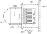
图20是用于说明根据本发明的又一实施例的发光二极管被应用于头灯的示例的剖面图。20 is a sectional view for explaining an example in which a light emitting diode according to still another embodiment of the present invention is applied to a headlight.
具体实施方式Detailed ways
以下,参照附图详细说明本发明的实施例。为了能够将本发明的思想充分传递给本领域技术人员,作为示例提供以下介绍的实施例。因此,本发明并不限定于如下所述的实施例,其可以具体化为其他形态。另外,在附图中,为了便利而可能夸张示出构成要素的宽度、长度、厚度等。并且,当记载为一个构成要素位于其他构成要素的“上部”或“上”时,不仅包括各个部分位于其他部分的“紧邻的上部”或“紧邻的上”的情况,还包括在各个构成要素与其他构成要素之间存在另外的构成要素的情形。在整个说明书中,相同的附图符号表示相同的构成要素。Hereinafter, embodiments of the present invention will be described in detail with reference to the drawings. In order to fully convey the idea of the present invention to those skilled in the art, the embodiments described below are provided as examples. Therefore, the present invention is not limited to the Examples described below, and may be embodied in other forms. In addition, in the drawings, the width, length, thickness, and the like of constituent elements may be exaggerated for convenience. In addition, when it is stated that one constituent element is located "on" or "on" another constituent element, it includes not only the case where each part is located "immediately above" or "immediately on" another part, but also the case where each constituent element is located When there is another constituent element between other constituent elements. Throughout the specification, the same reference numerals denote the same constituent elements.
根据本发明的一实施例的一种发光二极管包括:第一导电型半导体层;台面,位于所述第一导电型半导体层上,并包括活性层及第二导电型半导体层;透明的导电型氧化物层,布置在所述台面上,并与所述第二导电型半导体层电连接;介电层,覆盖所述导电型氧化物层,并具有使所述导电型氧化物层暴露的多个开口部,并具有比所述第二导电型半导体层及所述导电型氧化物层低的折射率;金属反射层,布置在所述介电层上,并通过所述介电层的开口部与所述导电型氧化物层连接;下部绝缘层,覆盖所述台面及所述金属反射层,并包括使所述第一导电型半导体层暴露的第一开口部及使所述金属反射层暴露的第二开口部;第一垫金属层,布置在所述下部绝缘层上,并通过所述第一开口部电连接于所述第一导电型半导体层;第二垫金属层,布置在所述下部绝缘层上,并通过所述第二开口部与所述金属反射层电连接;以及上部绝缘层,覆盖所述第一垫金属层及所述第二垫金属层,并具有使所述第一垫金属层暴露的第一开口部及使所述第二垫金属层暴露的第二开口部,所述介电层的厚度范围为所述第二导电型半导体层的厚度的4倍至13倍。A light emitting diode according to an embodiment of the present invention includes: a first conductivity type semiconductor layer; a mesa located on the first conductivity type semiconductor layer and including an active layer and a second conductivity type semiconductor layer; a transparent conductivity type semiconductor layer an oxide layer arranged on the mesa and electrically connected to the second conductivity type semiconductor layer; a dielectric layer covering the conductivity type oxide layer and having multiple layers exposing the conductivity type oxide layer an opening having a lower refractive index than the second conductivity type semiconductor layer and the conductivity type oxide layer; a metal reflective layer arranged on the dielectric layer and passing through the opening of the dielectric layer The part is connected to the conductive oxide layer; the lower insulating layer covers the mesa and the metal reflective layer, and includes a first opening that exposes the first conductive type semiconductor layer and exposes the metal reflective layer The exposed second opening; the first pad metal layer, arranged on the lower insulating layer, and electrically connected to the first conductivity type semiconductor layer through the first opening; the second pad metal layer, arranged on the on the lower insulating layer, and electrically connected to the metal reflective layer through the second opening; and an upper insulating layer, covering the first pad metal layer and the second pad metal layer, and having a The first opening exposing the first pad metal layer and the second opening exposing the second pad metal layer, the thickness range of the dielectric layer is 4 times the thickness of the second conductivity type semiconductor layer to 13 times.
所述介电层的厚度范围可以为200nm至1000nm,厚度范围具体可以为300nm至800nm。在此厚度范围内可以实现高的光输出及低的正向电压。The thickness of the dielectric layer may range from 200 nm to 1000 nm, specifically, the thickness range may range from 300 nm to 800 nm. High light output and low forward voltage can be achieved within this thickness range.
另外,所述导电型氧化物层的厚度范围可以为3nm至50nm,具体地,厚度范围可以为6nm至30nm。在此厚度范围内可以确保良好的欧姆接触电阻,并且可以减少光吸收所导致的损失。In addition, the thickness of the conductive oxide layer may range from 3 nm to 50 nm, specifically, the thickness range may range from 6 nm to 30 nm. Within this thickness range, good ohmic contact resistance can be ensured, and losses caused by light absorption can be reduced.
并且,所述介电层覆盖所述台面的侧面,并可以部分覆盖所述台面周围的第一导电型半导体层。In addition, the dielectric layer covers side surfaces of the mesa, and may partially cover the first conductivity type semiconductor layer around the mesa.
进一步,所述下部绝缘层可以覆盖所述介电层的边缘。Further, the lower insulating layer may cover edges of the dielectric layer.
另外,所述下部绝缘层的第一开口部沿着所述台面的周围使所述第一导电型半导体层暴露,所述第一垫金属层可以具有沿着所述台面周围与所述第一导电型半导体层接触的外部接触部。由于第一垫金属层沿着台面周围与第一导电型半导体层接触,因此可以提高发光二极管的电流分散性能。In addition, the first opening of the lower insulating layer exposes the first conductivity type semiconductor layer along the periphery of the mesa, and the first pad metal layer may have a The external contact portion where the conductive semiconductor layer contacts. Since the first pad metal layer is in contact with the first conductive type semiconductor layer along the periphery of the mesa, the current spreading performance of the light emitting diode can be improved.
并且,所述台面包括暴露所述第一导电型半导体层的凹入部,所述下部绝缘层的第一开口部可以在所述凹入部内还使所述第一导电型半导体层暴露。进而,所述第一垫金属层还可以包括在所述凹入部内与所述第一导电型半导体层接触的内部接触部。由于第一垫金属层在台面周围及台面内部与第一导电型半导体层接触,因此进一步加强发光二极管的电流分散性能。Also, the mesa includes a concave portion exposing the first conductive type semiconductor layer, and the first opening portion of the lower insulating layer may also expose the first conductive type semiconductor layer in the concave portion. Further, the first pad metal layer may further include an internal contact portion in the concave portion in contact with the first conductive type semiconductor layer. Since the first pad metal layer is in contact with the first conductive type semiconductor layer around the mesa and inside the mesa, the current spreading performance of the light emitting diode is further enhanced.
进一步,所述内部接触部可以与所述外部接触部连接,但本发明不限于此,内部接触部和外部接触部可以彼此相隔。Further, the internal contact part may be connected to the external contact part, but the present invention is not limited thereto, and the internal contact part and the external contact part may be separated from each other.
在若干实施例中,所述台面具有贯通所述第二导电型半导体层及活性层而使所述第一导电型半导体层暴露的过孔,所述下部绝缘层的第一开口部使被所述过孔暴露的第一导电型半导体层暴露,所述第一垫金属层可以具有与被所述过孔暴露的第一导电型半导体层接触的内部接触部。In several embodiments, the mesa has a via hole penetrating through the second conductive type semiconductor layer and the active layer to expose the first conductive type semiconductor layer, and the first opening of the lower insulating layer allows the The first conductive type semiconductor layer exposed by the via hole is exposed, and the first pad metal layer may have an internal contact portion in contact with the first conductive type semiconductor layer exposed by the via hole.
进一步,所述第一垫金属层包括在所述台面的外部与所述第一导电型半导体层接触的多个外部接触部,所述外部接触部可以彼此相隔。Further, the first pad metal layer includes a plurality of external contact portions contacting the first conductive type semiconductor layer outside the mesa, and the external contact portions may be separated from each other.
另外,所述发光二极管还可以包括:第一凸起垫,通过所述上部绝缘层的第一开口部与所述第一垫金属层连接;第二凸起垫,通过所述上部绝缘层的第二开口部与所述第二垫金属层连接。第一凸起垫及第二凸起垫在将发光二极管贴装于电路基板等而制作发光模块时可以被用作键合垫。In addition, the light emitting diode may further include: a first raised pad connected to the first pad metal layer through the first opening of the upper insulating layer; a second raised pad connected to the first pad metal layer through the upper insulating layer. The second opening is connected to the second pad metal layer. The first bump pad and the second bump pad can be used as bonding pads when mounting the light emitting diode on a circuit board or the like to manufacture a light emitting module.
进一步,所述下部绝缘层可以包括多个第二开口部,所述第二凸起垫可以覆盖所述下部绝缘层的至少一个第二开口部的上部。Further, the lower insulating layer may include a plurality of second openings, and the second raised pad may cover an upper portion of at least one second opening of the lower insulating layer.
所述第一凸起垫只要在与所述第二垫金属层绝缘的情况下其位置及形状可以多样地变形,并且第二凸起垫在与第一垫金属层绝缘的情况下其位置及形状也可以多样地变形。The position and shape of the first bump pad can be variously deformed as long as it is insulated from the second pad metal layer, and the position and shape of the second bump pad are insulated from the first pad metal layer. The shape can also be variously deformed.
另外,所述第二垫金属层可以被所述第一垫金属层围绕。因此可以在第一垫金属层和第二垫金属层之间形成使下部绝缘层暴露的边界区域。该边界区域可以被上部绝缘层所覆盖。In addition, the second pad metal layer may be surrounded by the first pad metal layer. A boundary region exposing the lower insulating layer may thus be formed between the first pad metal layer and the second pad metal layer. The boundary region may be covered by an upper insulating layer.
在若干实施例中,所述第二凸起垫可以限定于所述第二垫金属层的上部区域内而布置,但不限于此,所述第二凸起垫可以与所述第一垫金属层部分重叠。In several embodiments, the second raised pads may be arranged within the upper region of the second pad metal layer, but not limited thereto, and the second raised pads may be aligned with the first pad metal layer. Layers partially overlap.
另外,所述发光二极管还可以包括位于所述第一导电型半导体层一侧的基板。所述基板使从所述活性层生成的光透过。In addition, the light emitting diode may further include a substrate on one side of the first conductive type semiconductor layer. The substrate transmits light generated from the active layer.
根据本发明的另一实施例的一种发光二极管包括:第一导电型半导体层;台面,位于所述第一导电型半导体层上,包括活性层及第二导电型半导体层;透明的导电型氧化物层,布置在所述台面上,并与所述第二导电型半导体层电连接;介电层,覆盖所述导电型氧化物层,并具有使所述导电型氧化物层暴露的多个开口部,并具有比所述第二导电型半导体层及所述导电型氧化物层低的折射率;金属反射层,布置在所述介电层上,并通过所述介电层的开口部与所述导电型氧化物层连接;所述介电层具有低于所述导电型氧化物层及第二导电型半导体层的折射率且厚度范围为300nm至800nm。A light emitting diode according to another embodiment of the present invention includes: a first conductivity type semiconductor layer; a mesa, located on the first conductivity type semiconductor layer, including an active layer and a second conductivity type semiconductor layer; a transparent conductivity type semiconductor layer an oxide layer arranged on the mesa and electrically connected to the second conductivity type semiconductor layer; a dielectric layer covering the conductivity type oxide layer and having multiple layers exposing the conductivity type oxide layer an opening having a lower refractive index than the second conductivity type semiconductor layer and the conductivity type oxide layer; a metal reflective layer arranged on the dielectric layer and passing through the opening of the dielectric layer The portion is connected to the conductive oxide layer; the dielectric layer has a lower refractive index than the conductive oxide layer and the second conductive semiconductor layer and has a thickness ranging from 300nm to 800nm.
并且,所述介电层的厚度范围可以为所述第二导电型半导体层的厚度的4倍以上且13倍以下。In addition, the thickness range of the dielectric layer may be more than 4 times and less than 13 times the thickness of the second conductive type semiconductor layer.
另外,所述导电型氧化物层可以为铟锡氧化物(ITO)层,所述ITO层的厚度范围为6nm至30nm。In addition, the conductive oxide layer may be an indium tin oxide (ITO) layer, and the thickness of the ITO layer ranges from 6 nm to 30 nm.
所述发光二极管还可以包括:基板,位于所述第一导电型半导体层一侧;第一凸起垫,位于所述金属反射层的上部,并与所述第一导电型半导体层电连接;以及第二凸起垫,位于所述金属反射层的上部,并与所述金属反射层电连接。The light emitting diode may further include: a substrate located on one side of the first conductive type semiconductor layer; a first raised pad located on the upper part of the metal reflective layer and electrically connected to the first conductive type semiconductor layer; And the second raised pad is located on the upper part of the metal reflective layer and is electrically connected with the metal reflective layer.
根据本发明的又一实施例的一种发光二极管包括:第一导电型半导体层;台面,位于所述第一导电型半导体层上,并包括活性层及第二导电型半导体层;透明的导电型氧化物层,布置在所述台面上,并与所述第二导电型半导体层电连接;介电层,覆盖所述导电型氧化物层,并具有使所述导电型氧化物层暴露的多个开口部;金属反射层,布置在所述介电层上,并通过所述介电层的开口部与所述导电型氧化物层连接;下部绝缘层,覆盖所述台面及所述金属反射层,并包括使所述第一导电型半导体层暴露的第一开口部及使所述金属反射层暴露的第二开口部;第一垫金属层,布置在所述下部绝缘层上,并通过所述第一开口部电连接于所述第一导电型半导体层;第二垫金属层,布置在所述下部绝缘层上,并通过所述第二开口部与所述金属反射层电连接;上部绝缘层,覆盖所述第一垫金属层及所述第二垫金属层,并具有使所述第一垫金属层暴露的第一开口部及使所述第二垫金属层暴露的第二开口部,所述介电层的开口部包括与所述下部绝缘层的第一开口部中的至少一个相邻的宽度较窄且长的条形状的开口部。A light emitting diode according to yet another embodiment of the present invention includes: a first conductivity type semiconductor layer; a mesa located on the first conductivity type semiconductor layer and including an active layer and a second conductivity type semiconductor layer; a transparent conductive type oxide layer arranged on the mesa and electrically connected to the second conductive type semiconductor layer; a dielectric layer covering the conductive type oxide layer and having a layer that exposes the conductive type oxide layer A plurality of openings; a metal reflective layer arranged on the dielectric layer and connected to the conductive oxide layer through the openings of the dielectric layer; a lower insulating layer covering the mesa and the metal a reflective layer, including a first opening exposing the first conductive type semiconductor layer and a second opening exposing the metal reflective layer; a first pad metal layer arranged on the lower insulating layer, and Electrically connected to the first conductive type semiconductor layer through the first opening; a second pad metal layer, arranged on the lower insulating layer, and electrically connected to the metal reflective layer through the second opening an upper insulating layer covering the first pad metal layer and the second pad metal layer, and having a first opening exposing the first pad metal layer and a first opening exposing the second pad metal layer Two openings, the openings of the dielectric layer include narrow and long strip-shaped openings adjacent to at least one of the first openings of the lower insulating layer.
所述条状的开口部可布置为与下部绝缘层的第一开口部相邻,从而防止发光二极管由于电过载或静电放电而受损。The strip-shaped opening portion may be disposed adjacent to the first opening portion of the lower insulating layer, thereby preventing the light emitting diode from being damaged due to electrical overload or electrostatic discharge.
所述介电层可以包括所述条状开口部以外的其他形状的开口部,所述条状的开口部可以布置在相应的所述下部绝缘层的第一开口部与所述介电层的其他形状的开口部之间。The dielectric layer may include openings of other shapes than the strip-shaped openings, and the strip-shaped openings may be arranged between the corresponding first openings of the lower insulating layer and the openings of the dielectric layer. between openings of other shapes.
进一步,相应的所述下部绝缘层的第一开口部可以具有沿着一方向较长的形状,所述介电层的条状的开口部可以以与相应的所述下部绝缘层的第一开口部平行的方式布置。Further, the corresponding first openings of the lower insulating layer may have a long shape along one direction, and the strip-shaped openings of the dielectric layer may be aligned with the corresponding first openings of the lower insulating layer. Arranged in a parallel manner.
另外,所述介电层的条状的开口部可以比相应的所述下部绝缘层的第一开口部长。因此,可以提供对电过载或静电放电具有更好的抗性的发光二极管。In addition, the strip-shaped openings of the dielectric layer may be longer than the corresponding first openings of the lower insulating layer. Thus, light-emitting diodes with better resistance to electrical overload or electrostatic discharge can be provided.
另外,所述下部绝缘层可以具有在所述台面周围使所述第一导电型半导体层暴露的多个第一开口部,所述第一垫金属层可以在所述多个第一开口部与所述第一导电型半导体层接触。In addition, the lower insulating layer may have a plurality of first openings exposing the first conductive type semiconductor layer around the mesa, and the first pad metal layer may be formed between the plurality of first openings and the first conductive type semiconductor layer. The first conductive type semiconductor layer contacts.
在若干实施例中,所述介电层可以具有与所述多个第一开口部分别相邻的多个条状的开口部。In several embodiments, the dielectric layer may have a plurality of strip-shaped openings respectively adjacent to the plurality of first openings.
在若干实施例中,所述介电层的条状的开口部可以跨过所述外部接触部而较长地布置。In several embodiments, the strip-shaped openings of the dielectric layer can be arranged longer across the external contact.
所述发光二极管还可以包括:第一凸起垫;以及第二凸起垫,所述第一凸起垫和第二凸起垫分别通过所述上部绝缘层的第一开口部及第二开口部电连接于所述第一垫金属层及所述第二垫金属层,所述条状的开口部的至少一部分可以布置于所述第一凸起垫的下部。The light emitting diode may further include: a first raised pad; and a second raised pad, the first raised pad and the second raised pad respectively pass through the first opening and the second opening of the upper insulating layer The portion is electrically connected to the first pad metal layer and the second pad metal layer, and at least a part of the strip-shaped opening may be disposed under the first bump pad.
并且,所述条状的开口部的一部分也可以布置于所述第二凸起垫的下部。In addition, a part of the strip-shaped opening may be arranged under the second bump pad.
另外,所述发光二极管还可以包括位于所述第一导电型半导体层一侧的基板,所述基板使从所述活性层生成的光透过。In addition, the light emitting diode may further include a substrate on a side of the first conductive type semiconductor layer, and the substrate transmits light generated from the active layer.
另外,所述第一垫金属层可以沿着所述台面M的一侧边缘而具有突出部,所述第一垫金属层在所述台面的边缘附近具有与所述第一导电型半导体层接触的外部接触部,所述外部接触部借助所述突出部而形成,所述第一垫金属层的边缘中的所述突出部之间的区域可以位于所述导电型氧化物层上。In addition, the first pad metal layer may have a protruding portion along one side edge of the mesa M, and the first pad metal layer may have a protruding portion in contact with the first conductivity type semiconductor layer near the edge of the mesa M. The external contact part is formed by the protruding part, and the area between the protruding parts in the edge of the first pad metal layer may be located on the conductive oxide layer.
根据本发明的又一实施例的一种发光二极管包括:第一导电型半导体层;台面,位于所述第一导电型半导体层上,并包括活性层及第二导电型半导体层;透明的导电型氧化物层,布置在所述台面上,并与所述第二导电型半导体层电连接;介电层,覆盖所述导电型氧化物层,并具有使所述导电型氧化物层暴露的多个开口部;金属反射层,布置在所述介电层上,并通过所述介电层的开口部与所述导电型氧化物层连接;下部绝缘层,覆盖所述台面及所述金属反射层,并包括使所述第一导电型半导体层暴露的至少一个第一开口部及使所述金属反射层暴露的第二开口部;第一垫金属层,布置在所述下部绝缘层上,并通过所述至少一个第一开口部电连接于所述第一导电型半导体层;第二垫金属层,布置在所述下部绝缘层上,并通过所述第二开口部与所述金属反射层电连接;以及上部绝缘层,覆盖所述第一垫金属层及所述第二垫金属层,并具有使所述第一垫金属层暴露的第一开口部及使所述第二垫金属层暴露的第二开口部,所述介电层的开口部包括具有彼此不同的大小的开口部,与所述上部绝缘层的第一开口部相邻的所述介电层的开口部中的至少一个的宽度或长度大于从所述上部绝缘层的第一开口部更远地布置的所述介电层的至少一个其他开口部。A light emitting diode according to yet another embodiment of the present invention includes: a first conductivity type semiconductor layer; a mesa located on the first conductivity type semiconductor layer and including an active layer and a second conductivity type semiconductor layer; a transparent conductive type oxide layer arranged on the mesa and electrically connected to the second conductive type semiconductor layer; a dielectric layer covering the conductive type oxide layer and having a layer that exposes the conductive type oxide layer A plurality of openings; a metal reflective layer arranged on the dielectric layer and connected to the conductive oxide layer through the openings of the dielectric layer; a lower insulating layer covering the mesa and the metal A reflective layer, including at least one first opening exposing the first conductive type semiconductor layer and a second opening exposing the metal reflective layer; a first pad metal layer arranged on the lower insulating layer , and is electrically connected to the first conductive type semiconductor layer through the at least one first opening; the second pad metal layer is arranged on the lower insulating layer, and is connected to the metal layer through the second opening. The reflective layer is electrically connected; and an upper insulating layer covers the first pad metal layer and the second pad metal layer, and has a first opening that exposes the first pad metal layer and exposes the second pad A second opening in which the metal layer is exposed, the opening in the dielectric layer includes openings having different sizes from each other, and the opening in the dielectric layer adjacent to the first opening in the upper insulating layer At least one of the width or length is greater than at least one other opening portion of the dielectric layer disposed further from the first opening portion of the upper insulating layer.
通过使上部绝缘层的第一开口部,即,相邻于第一垫金属层与第一导电型半导体层所接触的区域的介电层的开口部大于其他介电层的开口部,可以提供具有对于电过载或静电放电强的抗性的发光二极管。By making the first opening of the upper insulating layer, that is, the opening of the dielectric layer adjacent to the region where the first pad metal layer is in contact with the first conductivity type semiconductor layer larger than the openings of other dielectric layers, it is possible to provide Light-emitting diodes with high resistance to electrical overload or electrostatic discharge.
在若干实施例中,所述具有更大的宽度或长度的所述介电层的开口部可以具有条(bar)形状。在其他实施例中,所述介电层的开口部可以具有圆形或环形状。In several embodiments, the opening portion of the dielectric layer having a greater width or length may have a bar shape. In other embodiments, the opening of the dielectric layer may have a circular or ring shape.
所述发光二极管还可以包括:第一凸起垫;以及第二凸起垫,所述第一凸起垫和第二凸起垫可以分别通过所述上部绝缘层的第一开口部及第二开口部电连接于所述第一垫金属层及所述第二垫金属层,所述具有更大的宽度或长度的所述介电层的开口部的至少一部分布置于所述第一凸起垫的下部。The light emitting diode may further include: a first raised pad; and a second raised pad, and the first raised pad and the second raised pad may respectively pass through the first opening and the second opening of the upper insulating layer. The opening is electrically connected to the first pad metal layer and the second pad metal layer, and at least a part of the opening of the dielectric layer having a greater width or length is arranged on the first protrusion lower part of the pad.
在一实施例中,所述具有更大的宽度或长度的所述介电层的开口部的至少一个可以从所述第一凸起垫的下部沿伸至所述第二凸起垫的下部。In one embodiment, at least one of the openings of the dielectric layer having a greater width or length may extend from the lower portion of the first raised pad to the lower portion of the second raised pad. .
在若干实施例中,所述台面可以具有使所述第一导电型半导体层暴露的过孔,所述下部绝缘层的第一开口部包括在所述过孔内使所述第一导电型半导体层暴露的开口部,所述第一垫金属层包括在所述过孔内与所述第一导电型半导体层接触的内部接触部,所述具有更大的宽度或长度的所述介电层的开口部可以与所述过孔相邻而布置。In several embodiments, the mesa may have a via hole exposing the first conductive type semiconductor layer, and the first opening of the lower insulating layer includes a via hole that exposes the first conductive type semiconductor layer. layer exposed opening, the first pad metal layer includes an internal contact portion in contact with the first conductivity type semiconductor layer in the via hole, and the dielectric layer having a greater width or length The opening portion of the via hole may be arranged adjacent to the via hole.
进一步,与所述过孔相邻而布置的所述介电层的开口部可以围绕所述孔。Further, the opening portion of the dielectric layer disposed adjacent to the via hole may surround the hole.
另外,所述第一垫金属层可以包括在所述台面的外部与所述第一导电型半导体层接触的外部接触部,所述外部接触部彼此相隔,所述具有更大的宽度或长度的所述介电层的开口部可以与所述外部接触部分别相邻而布置。In addition, the first pad metal layer may include an external contact part in contact with the first conductive type semiconductor layer outside the mesa, the external contact parts are spaced apart from each other, and the outer contact part having a larger width or length The opening portions of the dielectric layer may be arranged adjacent to the external contact portions, respectively.
另外,所述介电层可以具有低于所述第二导电型半导体层及所述导电型氧化物层的折射率,且厚度范围为300nm至800nm。并且,所述导电型氧化物层的厚度范围可以为3nm至50nm。In addition, the dielectric layer may have a lower refractive index than the second conductivity type semiconductor layer and the conductivity type oxide layer, and have a thickness ranging from 300 nm to 800 nm. Also, the thickness of the conductive oxide layer may range from 3nm to 50nm.
并且,所述发光二极管还可以包括位于所述第一导电型半导体层一侧的基板,所述基板使从所述活性层生成的光透过。Also, the light emitting diode may further include a substrate on a side of the first conductive type semiconductor layer, and the substrate transmits light generated from the active layer.
根据本发明的又一实施例的一种发光二极管包括:第一导电型半导体层;台面,位于所述第一导电型半导体层上,并包括活性层及第二导电型半导体层;透明的导电型氧化物层,布置在所述台面上,并与所述第二导电型半导体层电连接;介电层,覆盖所述导电型氧化物层,并具有使所述导电型氧化物层暴露的多个开口部;金属反射层,布置在所述介电层上,并通过所述介电层的开口部与所述导电型氧化物层连接;下部绝缘层,覆盖所述台面及所述金属反射层,并包括使所述第一导电型半导体层暴露的至少一个第一开口部及使所述金属反射层暴露的第二开口部;第一垫金属层,布置在所述下部绝缘层上,并通过所述至少一个第一开口部电连接于所述第一导电型半导体层;第二垫金属层,布置在所述下部绝缘层上,并通过所述第二开口部与所述金属反射层电连接;以及上部绝缘层,覆盖所述第一垫金属层及所述第二垫金属层,并具有使所述第一垫金属层暴露的第一开口部及使所述第二垫金属层暴露的第二开口部,所述介电层的开口部包括位于所述上部绝缘层的第一开口部的下部的开口部,位于所述上部绝缘层的第一开口部下部且与所述下部绝缘层的第一开口部相邻的开口部中的从所述第一开口部沿垂直方向相隔的开口部的相隔距离大于最靠近所述第一开口部的所述介电层的开口部的相隔距离。A light emitting diode according to yet another embodiment of the present invention includes: a first conductivity type semiconductor layer; a mesa located on the first conductivity type semiconductor layer and including an active layer and a second conductivity type semiconductor layer; a transparent conductive type oxide layer arranged on the mesa and electrically connected to the second conductive type semiconductor layer; a dielectric layer covering the conductive type oxide layer and having a layer that exposes the conductive type oxide layer A plurality of openings; a metal reflective layer arranged on the dielectric layer and connected to the conductive oxide layer through the openings of the dielectric layer; a lower insulating layer covering the mesa and the metal A reflective layer, including at least one first opening exposing the first conductive type semiconductor layer and a second opening exposing the metal reflective layer; a first pad metal layer arranged on the lower insulating layer , and is electrically connected to the first conductive type semiconductor layer through the at least one first opening; the second pad metal layer is arranged on the lower insulating layer, and is connected to the metal layer through the second opening. The reflective layer is electrically connected; and an upper insulating layer covers the first pad metal layer and the second pad metal layer, and has a first opening that exposes the first pad metal layer and exposes the second pad The second opening part where the metal layer is exposed, the opening part of the dielectric layer includes an opening part located at the lower part of the first opening part of the upper insulating layer, located at the lower part of the first opening part of the upper insulating layer and connected to the Among the openings adjacent to the first opening of the lower insulating layer, the openings separated from the first opening in the vertical direction are separated by a distance greater than the opening of the dielectric layer closest to the first opening. The distance between the parts.
通过调节第一垫金属层与第一导电型半导体层接触的接触部与相邻于该接触部的介电层的开口部的距离,可以提供对电过载或静电放电具有提高的抗性的发光二极管。By adjusting the distance between the contact portion where the first pad metal layer is in contact with the first conductive type semiconductor layer and the opening portion of the dielectric layer adjacent to the contact portion, it is possible to provide light emission with improved resistance to electrical overload or electrostatic discharge diode.
以下,参照附图对本发明的实施例进行具体的说明。Hereinafter, embodiments of the present invention will be specifically described with reference to the drawings.
图1是用于说明根据本发明的一实施例的发光二极管的示意性平面图,图2是沿着图1的截取线A-A截取的剖面图。1 is a schematic plan view illustrating a light emitting diode according to an embodiment of the present invention, and FIG. 2 is a cross-sectional view taken along line A-A of FIG. 1 .
参照图1及图2,所述发光二极管包括基板21、第一导电型半导体层23、活性层25、第二导电型半导体层27、导电型氧化物层28、介电层29、金属反射层31、下部绝缘层33、第一垫金属层35a、第二垫金属层35b及上部绝缘层37。进而,所述发光二极管还可以包括第一凸起垫39a及第二凸起垫39b。1 and 2, the light emitting diode includes a
所述基板21只要是能够使氮化镓系半导体层生长的基板,就不受特殊限制。作为基板21的示例,可以有蓝宝石基板、氮化镓基板、SiC基板等多种,并且可以是图案化的蓝宝石基板。基板21可以如图1所示地具有矩形或正方形的外形,但是不必受限于此。基板21的大小不受特殊限制,并且可以多样地选择。The
第一导电型半导体层23布置于基板21上。第一导电型半导体层23是在基板21上生长的层,可以是氮化镓系半导体层。第一导电型半导体层23可以是掺杂有杂质,例如Si的氮化镓系半导体层。The first conductive
在本实施例中,第一导电型半导体层23的边缘与基板21的边缘平行。但是,本发明并不限于此,第一导电型基板23可以位于被基板21的边缘围绕的区域内侧。在此情况下,基板21的上部面中的一部分区域可以沿着第一导电型半导体层23的周围而暴露。In this embodiment, the edge of the first conductive
在第一导电型半导体层23上布置有台面M。台面M可以限定于被第一导电型半导体层23围绕的区域内侧而布置。因此,第一导电型半导体层23的边缘附近区域不被台面M覆盖而暴露于外部。A mesa M is arranged on the first conductive
台面M包括第二导电型半导体层27和活性层25。所述活性层25存在于第一导电型半导体层23和第二导电型半导体层27之间。活性层25可以具有单量子阱或多量子阱结构。活性层25内的阱层的组成及厚度决定生成的光的波长,尤其,可以通过调节阱层的组成而提供生成紫外线、蓝色光或绿色光的活性层。The mesa M includes the second conductive
另外,第二导电型半导体层可以是掺杂有p型杂质,例如Mg的氮化镓系半导体层。第二导电型半导体层27的p型杂质的浓度影响第二导电型半导体层27的折射率。第二导电型半导体层27的p型杂质的浓度可以具有8×10-18~4×10-21/cm3的范围。在杂质的浓度低于8×10-18/cm3的情况下,无法得到增加折射率的效果,并且在高于4×10-21/cm3的情况下,难以形成稳定的欧姆接触。In addition, the second conductive type semiconductor layer may be a gallium nitride-based semiconductor layer doped with p-type impurities, such as Mg. The concentration of the p-type impurity of the second conductivity
尤其,第二导电型半导体层27内的p型杂质浓度可以不具有预定的值而具有在所述范围内随着厚度而变化的浓度属性。尤其,为了在第二导电型半导体层27的表面具有更高的折射率,在靠近导电型氧化物层28的一侧可以具有更高的杂质浓度。In particular, the p-type impurity concentration in the second conductivity
据此,可以通过增加第二导电型半导体层27的折射率而增加与导电型氧化物层28的折射率的差距,并且使第二导电型半导体层27和导电型氧化物层28之间的折射率差距与导电型氧化物层28和介电层29之间的折射率差距更加相似,从而进行高效的光提取。Accordingly, the gap between the refractive index of the second conductive
图3示出第二导电型半导体层27内的浓度属性。如图3所示,第二导电型半导体层27内的p型杂质(例如Mg)的浓度可以具有斜率彼此不同的区间。并且可以具有浓度在靠近活性层25的一侧减少且随着靠近导电型氧化物层28而增加的属性,尤其,浓度随着靠近导电型氧化物层28而急剧增加,从而可以具有比靠近活性层的一侧的浓度减少斜率的绝对值更大的斜率。据此,折射率急剧增加的部分与导电型氧化物层28相接而可以最大化光提取效果。FIG. 3 shows concentration profiles within the second conductivity
另外,第一导电型半导体层23及第二导电型半导体层27可以分别为单层,但不限于此,也可以是多层,并且也可以包括超晶格层。第一导电型半导体层23、活性层25及第二导电型半导体层27可以通过诸如金属有机化学气相生长法(MOCVD)或者分子束外延(MBE)等公知的方法在腔室内生长于基板21上而形成。In addition, the first conductive
另外,如图1所示,在所述台面M可以形成有向内部渗透的凹入部30,并且第一导电型半导体层23的上表面可以借助于凹入部30而暴露。凹入部30可以形成为从台面M的一侧边缘朝向与之相向的另一侧边缘而在台面M的内部较长地沿伸。凹入部30的长度不受特殊限制,并且可以等于或大于台面M长度的1/2。并且,在图1中示出了两个凹入部30,但是凹入部30的数量可以为1个或3个以上。随着凹入部30的数量增加,后述的第一垫金属层35a的内部接触部35a2的数量增加,从而改善电流分散性能。In addition, as shown in FIG. 1 , a
另外,凹入部30的宽度在末端部变长而具有圆弧形状。通过如此形成凹入部30的末端部形状,可以将下部绝缘层33以类似的形状图案化。尤其,在下部绝缘层33包括分布式布拉格反射器的情况下,如果宽度没有如图1所示地在末端部增加,则在分布式布拉格反射器的侧壁形成严重的双重台阶并且侧壁的倾斜角增加,因此第一垫金属层35a容易产生裂纹。因此,通过如本实施例一样形成凹入部30的末端部形状及下部绝缘层33的第一开口部33a2的末端部形状,可以使下部绝缘层33的边缘形成为具有缓慢的倾斜角,从而可以改善发光二极管的良率。In addition, the width of the recessed
在本实施例中,对于凹入部30形成于台面M的情形进行了图示及说明,但是代替凹入部30,台面M可以具有贯通第二导电型半导体层27及活性层25的至少一个过孔。In this embodiment, the situation where the recessed
另外,导电型氧化物层28布置在台面M上部而与第二导电型半导体层27接触。导电型氧化物层28可以在台面M上部区域布置于台面M的几乎全部区域。例如,导电型氧化物层28可以覆盖台面M上部区域的80%以上,或进一步地覆盖90%以上。In addition, the conductive
导电型氧化物层28形成为使在活性层25生成的光透过的氧化物层。导电型氧化物层28例如可以利用ITO(铟锡氧化物)或ZnO等来形成。导电型氧化物层28形成为足够与第二导电型半导体层27欧姆接触的厚度,例如可以在3nm至50nm的厚度范围内,具体为在6nm至30nm的厚度范围内形成。如果导电型氧化物层28的厚度过薄,则无法提供足够的欧姆特性,从而使正向电压增加。并且,如果导电型氧化物层28的厚度过厚,则产生光吸收引起的损失,从而降低发光效率。The
另外,介电层29覆盖导电型氧化物层28,进而,可以覆盖第二导电型半导体层27、活性层25及第一导电型半导体层23的侧面。介电层29的边缘可以被下部绝缘层33覆盖。因此,介电层29的边缘相比于下部绝缘层33的边缘而更远离基板21的边缘。但是,本发明不限于此,介电层29的一部分可以暴露于下部绝缘层33的外部。In addition, the
介电层29具有使导电型氧化物层28暴露的开口部29a。多个开口部29a可以布置于导电型氧化物层28的上部。开口部29a用作使金属反射层31与导电型氧化物层28连接的连接通道。并且,介电层29在台面M周围使第一导电型半导体层23暴露,并在凹入部30内使第一导电型半导体层23暴露。
介电层29由具有比第二导电型半导体层27及导电型氧化物层28低的折射率的绝缘物质形成。介电层29例如可以由SiO2形成。The
介电层29的厚度会影响发光二极管的正向电压以及光输出。介电层29的厚度可以具有200nm至1000nm范围内的厚度,具体可以具有300nm至800nm范围内的厚度。在介电层29的厚度小于200nm的情况下,正向电压较高而光输出较低而并不优秀。另外,如果介电层29的厚度超过400nm,则光输出饱和并表现出正向电压再次增加的倾向。因此,介电层29的厚度在不超过1000nm时有利,尤其可以为800nm以下。尤其,介电层29的厚度可以为活性层25上的第二导电型半导体层27的厚度的4倍以上,并且可以为13倍以下。The thickness of the
另外,金属反射层31布置于介电层29上而通过开口部29a与欧姆接触层28连接。金属反射层31包括反射性金属,例如可以包括Ag或Ni/Ag。进而,金属反射层32可以包括用于保护反射金属物质层的阻挡层,例如Ni。并且可以包括用于防止金属层的氧化的Au层。进而,为了提高Au层的粘合力,可以在Au层的下部包括Ti层。金属反射层31与介电层29的上表面相接,因此,所示介电层29的厚度等于导电型氧化物层28与金属反射层31之间的相隔距离。In addition, the metal
利用导电型氧化物层28形成欧姆接触并在介电层29上布置金属反射层31,从而可以防止欧姆电阻由于焊料等而变高。进一步地,通过将导电型氧化物层28、介电层29及金属反射层布置于第二导电型半导体层27上,可以提高光的反射率,因此可以改善发光效率。By forming an ohmic contact with the
下部绝缘层33覆盖台面M及金属反射层31。下部绝缘层还可以沿着台面M周围而覆盖第一导电型半导体层23,并且可以在台面M内部的凹入部30内覆盖第一导电型半导体层23。下部绝缘层33尤其覆盖台面M的侧面。下部绝缘层33还可以覆盖介电层29。The lower insulating
另外,下部绝缘层33具有使第一导电型半导体层暴露的第一开口部33a1、33a2及使金属反射层31暴露的第二开口部33b。第一开口部33a1沿着台面M的周围而使第一导电型半导体层23暴露,并且第一开口部33a2在所述凹入部30内使第一导电型半导体层23暴露。在代替凹入部30而形成过孔的情况下,第一开口部33a2在过孔内使第一导电型半导体层23暴露。In addition, the lower insulating
如图1所示,所述第一开口部33a1和第一开口部33a2可以彼此连接。但是,本发明不限于此,第一开口部33a1、33a2可以彼此相隔。As shown in FIG. 1 , the first opening portion 33a1 and the first opening portion 33a2 may be connected to each other. However, the present invention is not limited thereto, and the first opening parts 33a1, 33a2 may be spaced apart from each other.
本实施例中,下部绝缘层33的第一开口部33a1形成为使包括第一导电型半导体层23的边缘的周围区域全部暴露。但是,本发明不限于此,下部绝缘层33的第一开口部33a1可以沿着台面M的周围而形成为带状。在此情况下,第一导电型半导体层23的边缘可以被下部绝缘层33覆盖或与下部绝缘层33的边缘平行。In the present embodiment, the
第二开口部33b使金属反射层31暴露。可以形成多个第二开口部33b,并且这些第二开口部33b可以与所述凹入部30相向而布置于基板21的一侧边缘附近。在下文中对第二开口部33b的位置再次进行说明。The
另外,下部绝缘层33可以形成为SiO2或Si3N4的单层,但不限于此。例如,下部绝缘层33可以具有包括氮化硅膜和氧化硅膜的多层结构,并且可以包括将氧化硅膜和氧化钛膜交替层叠的分布式布拉格反射器。In addition, the lower insulating
另外,第一垫金属层35a布置于所述下部绝缘层33上,并且可以借助下部绝缘层33而与台面M及金属反射层31绝缘。第一垫金属层35a可以通过下部绝缘层33的第一开口部33a1、33a2与第一导电型半导体层23接触。第一垫金属层35a可以包括沿着台面M周围而与第一导电型半导体层23接触的外部接触部35a1以及在所述凹入部30或过孔内与第一导电型半导体层23接触的内部接触部35a2。外部接触部35a1可以沿着台面M的周围而在基板21的边缘附近与第一导电型半导体层23接触,并且内部接触部35a2可以在被外部接触部35a1围绕的区域内部与第一导电型半导体层23接触。外部接触部35a1和内部接触部35a2可以彼此连接,但不限于此,也可以彼此相隔。并且,外部接触部35a1可以沿着台面M周围而连续地与第一导电型半导体层23接触,但不限于此,多个外部接触部35a1可以彼此相隔布置。In addition, the first
另外,第二垫金属层35b在下部绝缘层33上布置于台面M的上部区域,并且通过下部绝缘层33的第二开口部33b而与金属反射层31电连接。第二垫金属层35b可以被第一垫金属层35a围绕,并且可以在其间形成边界区域35ab。下部绝缘层33在边界区域35ab暴露,并且该边界区域35ab被后述的上部绝缘层37覆盖。In addition, the second
第一垫金属层35a和第二垫金属层35b可以通过同一工序利用同一材料一同形成。第一垫金属层35a和第二垫金属层35b可以包括如Al层的欧姆反射层,欧姆反射层可以形成在Ti、Cr或Ni等的粘合层上。并且,可以在所述欧姆反射层上形成Ni、Cr、Au等的单层或复合层结构的保护层。第一垫金属层35a和第二垫金属层35b例如可以具有Cr/Al/Ni/Ti/Ni/Ti/Au/Ti的多层结构。The first
上部绝缘层37覆盖第一垫金属层35a和第二垫金属层35b。并且,上部绝缘层37可以沿着台面M的周围而覆盖第一导电型半导体层23。本实施例中,上部绝缘层37可以沿着基板21的边缘而使第一导电型半导体层23暴露。但是,本发明不限于此,上部绝缘层37可以将第一导电型半导体层23全部覆盖,并且可以与基板21的边缘平行。The upper insulating
另外,上部绝缘层37具有使第一垫金属层35a暴露的第一开口部37a及使第二垫金属层35b暴露的第二开口部37。第一开口部37a及第二开口部37b可以布置在台面M的上部区域,并且可以彼此相向地布置。尤其,第一开口部37a及第二开口部37b可以靠近台面M的两侧边缘而布置。In addition, the upper insulating
上部绝缘层37可以形成为SiO2或Si3N4的单层,但不限于此。例如,上部绝缘层37可以具有包括氮化硅膜和氧化硅膜的多层结构,并且可以包括将氧化硅膜和氧化钛膜交替层叠的分布式布拉格反射器。The upper insulating
另外,第一凸起垫39a与通过上部绝缘层37的第一开口部37a暴露的第一垫金属层35a电接触,第二凸起垫39b与通过第二开口部37b暴露的第二垫金属层35b电接触。如图1所示,第一凸起垫39a可以布置于上部绝缘层37的第一开口部37a内,第二凸起垫39b可以布置于上部绝缘层37的第二开口部37b内。但是,本发明不限于此,第一凸起垫39a和第二凸起垫39b可以分别将第一开口部37a及第二开口部37b全部覆盖而进行密封。并且,所述第二凸起垫39b可以覆盖下部绝缘层33的第二开口部33b的上部区域。第二凸起垫39b可以将下部绝缘层33的第二开口部33b全部覆盖,但不限于此,开口部33b中的一部分可以位于第二凸起垫39b的外部。In addition, the
并且,如图1所示,第二凸起垫39b可以限定于第二垫金属层35a的上部区域内而布置。但是,本发明不限于此,第二凸起垫39b的一部分可以与第一垫金属层35a重叠。但是,上部绝缘层37可以布置于第一垫金属层35a和第二凸起垫39b之间而使第一垫金属层35a和第二凸起垫39b绝缘。Also, as shown in FIG. 1 , the
根据本发明的实施例,代替现有的欧姆反射层而使用导电型氧化物层28、介电层29及金属反射层31的反射结构。因此,可以防止焊料等结合材料渗透至接触区域,并且可以确保稳定的欧姆接触电阻而提高发光二极管的可靠性。并且,可以使介电层29的厚度为300nm以上而实现高的光输出及低的正向电压。According to an embodiment of the present invention, the reflective structure of the
图4a及图4b为示出导电型氧化物层28为ITO并介电层29为SiO2,以及根据SiO2的厚度的正向电压Vf及光输出Po的图表。4a and 4b are graphs showing the
ITO的厚度为20nm,并且将SiO2变为200nm、400nm、600nm及800nm。第二导电型半导体层27的厚度大约为65nm。The thickness of ITO is 20nm, and SiO2 is changed to 200nm, 400nm, 600nm and 800nm. The thickness of the second conductivity
如图4a所示,当介电层29的厚度为200nm时,正向电压相对较高,并且在400nm表现出最低值。并且,当厚度在400nm以上变大时,表现出了正向电压增加的倾向。As shown in FIG. 4a, when the thickness of the
另外,如图4b所示,当介电层29的厚度为200nm时表现出最低的光输出,并且在400nm以上时表现出大致类似的光输出。In addition, as shown in FIG. 4b, the lowest light output is exhibited when the thickness of the
图5是用于说明根据本发明的又一实施例的发光二极管的示意性平面图,图6是沿着图5的截取线B-B截取的剖面图。5 is a schematic plan view illustrating a light emitting diode according to still another embodiment of the present invention, and FIG. 6 is a cross-sectional view taken along line B-B of FIG. 5 .
参照图5及图6,根据本实施例的发光二极管与参照图1及图2说明的发光二极管大致类似,因此为了避免重复说明,以下主要对特征性的区别点进行说明。Referring to FIG. 5 and FIG. 6 , the light emitting diode according to this embodiment is substantially similar to the light emitting diode described with reference to FIG. 1 and FIG. 2 , so in order to avoid repeated description, the following mainly describes the characteristic differences.
首先,在前一实施例中,第一导电型半导体层23的边缘与基板21的边缘平行,但是,本实施例中,第一导电型半导体层23的边缘布置于被基板21的边缘围绕的区域内。因此,基板21的边缘附近的区域暴露于第一导电型半导体层23的外部。First of all, in the previous embodiment, the edge of the first conductive
并且,在本实施例中,介电层29的开口部29a的位置被控制,并且在下文中对此进行说明。Also, in the present embodiment, the position of the
另外,在前一实施例中,下部绝缘层33的边缘位于第一导电型半导体层23上,但是,本实施例中,下部绝缘层33覆盖第一导电型半导体层23的边缘,并与基板21的边缘平行。下部绝缘层33的第一开口部33a1限定于第一导电型半导体层23上而布置,并且沿着台面M的周围而以环状布置。In addition, in the previous embodiment, the edge of the lower insulating
进而,下部绝缘层33的第二开口部33b形成于第二凸起垫39b的外部以不与第二凸起垫39b重叠。通过使第二开口部33b与第二凸起垫39b沿水平方向相隔而布置,可以在焊接第二凸起垫39b时防止焊料向发光二极管的内部扩散。Furthermore, the
第一垫金属层35a覆盖下部绝缘层33的第一开口部33a1而与第一导电型半导体层23接触,据此,在所述第一开口部33a1内形成外部接触部35a1。如前一实施例所述,外部接触部35a1可以与内部接触部35a2连接或与内部接触部35a2相隔。The first
另外,在本实施例中,第二垫金属层35b的形状相比于图1的实施例而存在差异,因此,第二垫金属层35b与第一垫金属层35a之间的边界区域35ab的位置也与图1的实施例存在差异。如图5所示,第二垫金属层35b向内部接触部35a2和外部接触部35a1之间的区域沿伸。在布置有多个内部接触部35a2的情况下,如图所示,第二垫金属层35b的前端可以具有凹凸形状。第一垫金属层35a可以与第二垫金属层35b以预定的间距相隔,因此,与第二垫金属层35b的前端相邻的第一垫金属层35a也具有凹凸形状。In addition, in this embodiment, the shape of the second
通过将第二垫金属层35b的前端向内部接触部35a2的附近沿伸,可以容易地使下部绝缘层33的第二开口部33b与第二凸起垫39b沿水平方向相隔。By extending the tip of the second
另外,上部绝缘层37覆盖下部绝缘层33,并且上部绝缘层37的边缘可以与基板21及下部绝缘层33的边缘平行地形成。进而,在上述实施例中,虽然以第一凸起垫39a及第二凸起垫39b以限定于上部绝缘层37的第一开口部37a及第二开口部37b内的方式布置的情形进行图示及说明,但是在本实施例中,第一凸起垫39a及第二凸起垫39b覆盖上部绝缘层37的第一开口部37a和第二开口部37b而进行密封。即,第一凸起垫39a及第二凸起垫39b的边缘位于上部绝缘层37的上表面上。据此,可以防止第一垫金属层35a及第二垫金属层35b在上部绝缘层37与凸起垫39a、39b之间暴露。据此,可以防止焊料直接向第一垫金属层35a及第二垫金属层35b扩散。In addition, the upper insulating
本实施例中,对第一导电型半导体层23、下部绝缘层33、上部绝缘层37及凸起垫39a、39b的边缘位置不同于图1的实施例的情形进行了说明,但这是为了说明相对于图1的实施例而可变形的实施例,本实施例不限于在此说明的事项。即,在本实施例中,第一导电型半导体层23、下部绝缘层33及上部绝缘层37的边缘位置可以与图1的实施例相同,并且,可以将图1的实施例如本实施例地变形。In this embodiment, the case where the edge positions of the first conductivity
另外,在本实施例中,为了加强相对于电过载或静电放电的抗性而调节介电层29的开口部29a的位置。导电型氧化物层28、介电层29及金属反射层31的反射结构提高反射率,但是导电型氧化物层28与金属反射层31需要电连接。介电层29的开口部29a提供金属反射层电连接于导电型氧化物层28的通道。并且,为了将电流均匀地分散至导电型氧化物层28的宽的区域,多个开口部29a在导电型氧化物层28上较宽地分布。但是,与第一垫金属层相接的外部接触部35a1及内部接触部35a2与开口部29a的距离可能会影响发光二极管对于电过载或静电放电的特性。In addition, in the present embodiment, the position of the opening
作为对此的对策,如图5所示,本实施例的特征在于,使位于上部绝缘层37的第一开口部37a区域下部(或者第一凸起垫39a的下部)的介电层29的开口部29a中的最靠近外部接触部35a1及内部接触部35a2的开口部29a相对远离。As a countermeasure against this, as shown in FIG. 5, the present embodiment is characterized in that the
即,图5中,外部接触部35a1与位于上部绝缘层37的第一开口部37a下部的开口部29a之间的最短距离Dv1大于外部接触部35a1与位于上部绝缘层37的第一开口部37a的外部的开口部29a之间的最短距离Ds。在附图中,表示外部接触部35a1与开口部29a之间的距离,但同样应用于内部接触部35a2与开口部29a之间的距离。That is, in FIG. 5 , the shortest distance Dv1 between the external contact portion 35a1 and the
位于电连接于第一导电型半导体层23的第一凸起垫39a的下部的介电层29的开口部29a与接触部35a1、35a2之间的距离受电过载或静电放电的较大的影响。因此,可以通过使位于第一凸起垫39a的下部的介电层29的开口部29a远离接触部35a1、35a2而提高发光二极管的可靠性。The distance between the
另外,除了第一凸起垫39a的下部,还可以使第二凸起垫39b的下部及其他位置的开口部29a与接触部35a1、35a2远离,但是可能无法使电流较宽地分散而降低发光效率。因此,在本实施例中,通过仅将位于第一凸起垫39a下部的开口部29a相比于其他开口部而相对较远地布置,可以不降低电流分散性能并改善静电放电特性。In addition, in addition to the lower part of the
图7是用于说明根据本发明的又一实施例的发光二极管的示意性平面图。FIG. 7 is a schematic plan view for explaining a light emitting diode according to still another embodiment of the present invention.
参照图7,根据本实施例的发光二极管与参照图5及图6说明的发光二极管大致类似,但区别在于,介电层29的开口部与多个开口部29a一同包括较长的形状的开口部29b。Referring to FIG. 7, the light emitting diode according to this embodiment is substantially similar to the light emitting diode described with reference to FIGS.
如果开口部29b位于外部接触部35a1及内部接触部35a2与开口部29a之间,则沿着外部接触部35a1及内部接触部35a2而形成闭环。与外部接触部35a1及内部接触部35a2相邻的开口部29b沿着接触部35a1、35a2而较长地相邻,因此可以防止在特定地点产生较大的电压差异,因此,可以提供对于电过载或静电放电具有较强抗性的发光二极管。When the
在本实施例中,开口部29b形成闭环,虽未图示,但是长度大于宽度的较长形状的开口部29b可以沿着接触部35a1、35a2排列。In this embodiment, the
另外,本实施例中,对于开口部29b不限于第一凸起垫39a的下部而还向第一凸起垫39a的外部沿伸的情形进行了说明,但是可以以限定于第一凸起垫39a的下部的方式布置。In addition, in this embodiment, the case where the
图8是用于说明根据本发明的又一实施例的发光二极管的示意性平面图。FIG. 8 is a schematic plan view for explaining a light emitting diode according to still another embodiment of the present invention.
参照图8,根据本实施例的发光二极管与参照图7说明的发光二极管大致类似,但区别在于,介电层29的开口部还包括开口部29c。Referring to FIG. 8 , the light emitting diode according to this embodiment is substantially similar to the light emitting diode described with reference to FIG. 7 , but the difference is that the opening portion of the
开口部29c位于被开口部29b围绕的区域内,尤其,可以位于第二凸起垫39b的下部区域外部。开口部29c的一部分也可以位于第一凸起垫39a的下部。The opening
图9是用于说明根据本发明的又一实施例的发光二极管的示意性平面图。FIG. 9 is a schematic plan view for explaining a light emitting diode according to still another embodiment of the present invention.
参照图9,根据本实施例的发光二极管与参照图5说明的发光二极管大致类似,但区别在于,台面M具有沿着一个轴方向的较长的形状,并且外部接触部35a1在没有内部接触部35a2的情况下形成于台面的一侧边缘附近,并且,第一垫金属层35a以不围绕第二垫金属层35b的方式形成。Referring to FIG. 9, the light emitting diode according to the present embodiment is substantially similar to the light emitting diode explained with reference to FIG. 35a2 is formed near one edge of the mesa, and the first
台面M具有沿着一个轴方向的较长的形状,例如,其长度可以为宽度的4倍以上,并且可以为7倍以下。通过使台面M形成为沿着一个轴方向较长的形状,可以相对减少第一垫金属层35a与第一导电型半导体层23接触的区域,因此可以确保发光面积。The mesa M has a long shape along one axis, for example, the length may be 4 times or more and 7 times or less the width. By forming the mesa M in a long shape along one axis, the contact area between the first
另外,台面M的一侧边缘可以形成为具有凹陷或凸出部。In addition, one side edge of the mesa M may be formed to have a depression or a protrusion.
介电层29覆盖导电型氧化物层28并覆盖台面M的侧面。如参照图5的说明,介电层29的一部分部分覆盖在台面M的周围暴露的第一导电型半导体层23。The
另外,介电层29具有使导电型氧化物层28暴露的多个开口部29a,并且为了改善对于电过载及静电放电的抗性而调节开口部29a的位置。在下文中对此进行再次的说明。In addition, the
金属反射层31布置于介电层29上,并且通过介电层29的开口部29a而与导电型氧化物层28连接。The metal
在本实施例中,导电型氧化物层28及金属反射层31覆盖台面M的上表面的大部分。但是,导电型氧化物层28及金属反射层31的边缘与台面M的边缘相隔,尤其,与相邻于外部接触部35a1的台面M的一侧边缘相隔更远。尤其,通过使导电型氧化物层28的边缘与接触部35a1相隔更远,可以防止由电过载或静电放电引起的元件不良的产生。In this embodiment, the
下部绝缘层33覆盖介电层29及金属反射层31,并且可以覆盖在台面M的周围暴露的第一导电型半导体层23的一部分。下部绝缘层33在台面M的凹陷区域使第一导电型半导体层23暴露。并且,下部绝缘层33可以覆盖第一导电型半导体层23,但是如图所示,也可以形成为使第一导电型半导体层23的边缘附近暴露。下部绝缘层33还具有使金属反射层31暴露的第二开口部33b。The lower insulating
另外,在本实施例中,第一垫金属层35a的除了形成外部接触部35a1的区域以外的部分布置于台面M上部。与图5的实施例的区别在于,图5的实施例中,第一垫金属层35a覆盖台面M的上部区域及侧面,并覆盖台面M周围的第一导电型半导体层23的一部分。并且,第一垫金属层35a的边缘可以在台面M的凹陷之间的区域位于台面M上。In addition, in the present embodiment, the portion of the first
并且,第一垫金属层35a可以包括具有偏向于台面M的一侧的较宽宽度的区域以及从该区域沿伸的具有较窄宽度的区域。外部接触部35a1沿着台面M的一侧边缘而形成,并且可以形成于在台面M的一侧边缘形成的凹陷内。外部接触部35a1可以形成为具有沿着台面M的长度方向较长的形状。并且,如图所示,外部接触部35a1可以借助第一垫金属层35a的具有较宽宽度的区域以及具有较窄宽度的区域而形成。Also, the first
第一垫金属层35a可以沿着台面M的一侧边缘而具有突出部,并且这些突出部可以形成外部接触部35a1。并且,第一垫金属层35a的边缘中的所述突出部之间的区域可以位于台面M上,进而可以位于导电型氧化物层28上。The first
另外,第二垫金属层35b可以布置在台面M的上部区域内。第二垫金属层35b可以沿着第一垫金属层35a的具有较窄宽度的区域而较长地形成。第二垫金属层35b可以通过下部绝缘层33的第二开口部33b而电连接于金属反射层31。下部绝缘层33的第二开口部33b也可以布置于第二凸起垫39b的下部,但是如图所示,可以与第二凸起垫39b沿水平方向相隔而布置。In addition, the second
本实施例中,介电层29的开口部29a与台面M的边缘相隔而布置,尤其,与相邻于外部接触部35a1的台面M的边缘相隔更远。尤其,位于第一凸起垫39a的下部的开口部29a中,与一个外部接触部35a1沿着垂直方向相隔最近的开口部29a的相隔距离Dv1大于与该外部接触部35a1相隔最近的开口部29a的相隔距离Ds。进而,相隔外部接触部35a1最近的开口部29a相比于最靠近台面M的边缘的开口部而更远离台面M的边缘而布置。In this embodiment, the
不仅可以调节位于第一凸起垫39a的下部的开口部29a的位置,还可以调节位于第二凸起垫39b的下部的开口部29a的位置,并且位于第一凸起垫39a和第二凸起垫39b下部的开口部29a的位置也可以被调节。即,如图9所示,与外部接触部35a1沿着垂直方向相隔的开口部29a的相隔距离Dv2可以大于与该外部接触部35a1相隔最近的开口部29a的相隔距离Ds。布置于第二凸起垫39b下部的开口部29a也可以如图所示地相同地布置。Not only the position of the
图10是用于说明根据本发明的又一实施例的发光二极管的示意性平面图。FIG. 10 is a schematic plan view for explaining a light emitting diode according to still another embodiment of the present invention.
参照图10,根据本实施例的发光二极管与参照图9说明的发光二极管大致类似,但区别在于,介电层29具有彼此不同的大小地开口部29a、129a。Referring to FIG. 10, the light emitting diode according to this embodiment is substantially similar to the light emitting diode described with reference to FIG. 9, but the difference is that the
本实施例中,相对较大的开口部129a相比于较小的开口部29a而更靠近外部接触部35a1而布置。尤其,在第一凸起垫39a的下部区域,开口部129a相比于开口部29a更靠近外部接触部35a1而布置。进而,在第二凸起垫39b的下部区域及其他区域,开口部129a可以比开口部29a更靠近外部接触部35a1而布置。In this embodiment, the relatively larger opening portion 129a is arranged closer to the external contact portion 35a1 than the
相对大的开口部129a防止电流集中于特定地点,从而提高对于电过载或静电放电的发光二极管的抗性。The relatively large opening portion 129a prevents current from concentrating on a specific place, thereby improving the resistance of the light emitting diode to electrical overload or electrostatic discharge.
本实施例中,虽然对开口部129a为圆形的情形进行了图示,但是其形状可以多样。尤其,开口部129a可以具有沿着台面M的长度方向较长的形状,例如可以具有椭圆形状或条状。In this embodiment, although the case where the opening part 129a is circular is shown in figure, it can have various shapes. In particular, the opening 129a may have a long shape along the longitudinal direction of the mesa M, for example, may have an oval shape or a strip shape.
图11是用于说明根据本发明的又一实施例的发光二极管的示意性平面图。FIG. 11 is a schematic plan view for explaining a light emitting diode according to still another embodiment of the present invention.
参照图11,根据本实施例的发光二极管与参照图10说明的发光二极管大致类似,但区别在于,条状的开口部129b与外部接触部35a1相邻而布置。Referring to FIG. 11 , the light emitting diode according to the present embodiment is substantially similar to the light emitting diode described with reference to FIG. 10 , but differs in that a strip-shaped
尤其,在第一凸起垫39a的下部布置有条状的开口部129b,进而,在第二凸起垫39b的下部及其他区域也可以布置有条状的开口部129b。条状的开口部129b可以与下部绝缘层33的第一开口部33a或外部接触部35a1平行地布置。In particular, strip-shaped
所述开口部129b布置于外部接触部35a1和开口部29a之间,并且防止电流集中于特定地点而提高对于电过载或静电放电的发光二极管的抗性。条状的开口部129b的末端以具有相对宽的宽度的方式形成,从而可以使图案化容易。The
图12是用于说明根据本发明的又一实施例的发光二极管的示意性平面图。FIG. 12 is a schematic plan view for explaining a light emitting diode according to still another embodiment of the present invention.
参照图12,根据本实施例的发光二极管与参照图11说明的发光二极管大致类似,但区别在于,一个条状的开口部129c跨过外部接触部35a1而连续形成。条状的开口部129c没必要是直线。尤其,位于第一凸起垫39a的下部区域的开口部129c的部分可以比其他部分更远离外部接触部35a1而布置。Referring to FIG. 12 , the light emitting diode according to this embodiment is substantially similar to the light emitting diode described with reference to FIG. 11 , but differs in that a strip-shaped
图13是用于说明根据本发明的又一实施例的发光二极管的示意性平面图,图14是沿着图13的截取线C-C截取的示意性剖面图。FIG. 13 is a schematic plan view illustrating a light emitting diode according to still another embodiment of the present invention, and FIG. 14 is a schematic cross-sectional view taken along line C-C of FIG. 13 .
参照图13及图14,根据本实施例的发光二极管与上文中说明的发光二极管大致类似,但区别在于,形成多个发光单元C1、C2,并且这些发光单元C1、C2串联连接。Referring to FIG. 13 and FIG. 14 , the light emitting diode according to this embodiment is substantially similar to the light emitting diode described above, but the difference is that a plurality of light emitting cells C1 and C2 are formed and these light emitting cells C1 and C2 are connected in series.
第一发光单元C1及第二发光单元C2布置于基板21上。第一发光单元C1及第二发光单元C2借助于暴露基板21的分离区域I而彼此分离。因此,第一发光单元C1和第二发光单元C2的半导体层彼此相隔。第一发光单元C1及第二发光单元C2彼此相隔而布置,并且可以分别具有正方形或矩形形状。尤其,第一发光单元C1及第二发光单元C2可以沿着彼此相向的方向而具有较长的矩形形状。The first light emitting unit C1 and the second light emitting unit C2 are arranged on the
分离区域I使发光单元C1、C2彼此分离。据此,基板21的表面在分离区域I通过半导体层而暴露。分离区域I通过光刻及蚀刻工序而形成,形成具有缓慢的倾斜面的光刻胶图案并将其用作掩膜而蚀刻半导体层而能够在分离区域I形成相对缓慢的倾斜的侧面。The separation region I separates the light emitting cells C1, C2 from each other. Accordingly, the surface of the
发光单元C1、C2隔着所述分离区域I而彼此相向。彼此相向的发光单元C1、C2的侧面被定义为内侧面,除此之外的侧面被定义为外侧面。因此,第一发光单元C1及第二发光单元C2内的第一导电型半导体层23也分别包括内侧面及外侧面。例如,第一导电型半导体层23可以包括一个内侧面和3个外侧面。The light emitting cells C1 and C2 face each other with the separation region I interposed therebetween. The side surfaces of the light-emitting cells C1 and C2 facing each other are defined as inner surfaces, and the other sides are defined as outer surfaces. Therefore, the first conductive
在各个第一导电型半导体层23上布置有台面M。台面M可以限定于被第一导电型半导体层23围绕的区域内侧而布置,因此,与第一导电型半导体层23的外侧面相邻的边缘附近区域不被台面M覆盖而暴露于外部。在其他实施例中,在分离区域I的侧壁,台面M的侧面和第一导电型半导体层23的侧面可以彼此连续。Mesas M are arranged on the respective first conductive type semiconductor layers 23 . The mesa M may be arranged inside a region surrounded by the first conductive
各个台面M包括第二导电型半导体层27和活性层25。所述活性层25存在于第一导电型半导体层23和第二导电型半导体层27之间。各个台面M具有凹陷,并且如下文所述,在该凹陷内形成下部绝缘层33的第一开口部33a,并且形成第一开口部33a内的外部接触部35a1。Each mesa M includes a second conductive
另外,在各个台面M上布置有导电型氧化物层28,并且介电层29覆盖各个发光单元C1、C2上的导电型氧化物层28及台面M。导电型氧化物层28与第二导电型半导体层27欧姆接触。导电型氧化物层28可以在台面M的上部区域遍布台面M的几乎整个区域而布置。但是,导电型氧化物层28可以与台面M的边缘相隔。In addition, a
介电层29覆盖台面M的上部区域及侧面,并且可以覆盖在台面M的周围暴露的第一导电型半导体层。介电层29还具有开口部29a、129b,并且条状的开口部129b可以布置于外部接触部35a1与不同的开口部29a之间。在本实施例中,以条状的开口部129a作为一例进行了图示及说明,但是除了条状以外,可以布置具有比开口部29a更大的大小的圆形、椭圆形或其他形状的开口部,并且连续地较长地沿伸的单个线形状的开口部可以布置于各个台面M上。The
金属反射层31布置于介电层29上,并且通过介电层29的开口部29a、129b与导电型氧化物层28连接。金属反射层31布置在各个发光单元C1、C2的台面M上部区域内。The metal
下部绝缘层33覆盖台面M,并且覆盖金属反射层31及介电层29。下部绝缘层33还覆盖在介电层29的外部暴露的第一导电型半导体层23及基板21。在基板21为图案化的蓝宝石基板的情况下,下部绝缘层33可以沿着基板21上的突出部的形状而形成。The lower insulating
下部绝缘层33具有在各个台面M的凹陷内使第一导电型半导体层23暴露的第一开口部33a,并且具有在第二发光单元上使金属反射层31暴露的第二开口部33b1以及在第一发光单元C1上使金属反射层31暴露的第三开口部33b2。第一开口部33a沿着台面M的外侧面而使第一导电型半导体层23暴露,并且第三开口部33b2在分离区域I附近使第一发光单元C1上的金属反射层31暴露。第三开口部33b2可以大致具有沿着分离区域I而较长的形状,但不限于此,可以具有多种形状。The lower insulating
另外,第二开口部33b1位于第二发光单元C2上,并且可以位于第二凸起垫39b的下部区域内。但是,在其他实施例中,第二开口部33b1可以在第二发光单元C2上与第二凸起垫39b沿着水平方向相隔而布置。In addition, the second opening part 33b1 is located on the second light emitting unit C2, and may be located in a lower region of the
另外,第一垫金属层35a、第二垫金属层35b及连接金属层35c布置于下部绝缘层33上。In addition, the first
第一垫金属层35a布置于第一发光单元C上,并与在台面M周围暴露的第一导电型半导体层23欧姆接触。如图13良好地示出,第一垫金属层35a沿着台面M的周围而通过下部绝缘层33的第一开口部33a而与第一导电型半导体层23欧姆接触,从而可以形成外部接触部35a1。附图中示出了第一垫金属层35a沿着台面M的周围而在台面M的凹陷内与第一导电型半导体层23断续地接触的情形,但是本发明不限于此,可以连续地接触。即,下部绝缘层33形成为具有沿着台面M的周围而使第一导电型半导体层23连续暴露的第一开口部33a,并且第一垫金属层35a可以通过下部绝缘层33的第一开口部33a而与第一导电型半导体层23连续接触。The first
另外,介电层29的条状开口部129b可以与下部绝缘层33的第一开口部33a平行,因此,可以与外部接触部35a1平行。In addition, the strip-shaped
第二垫金属层35b布置于第二发光单元C2上,且可以通过下部绝缘层33的第二开口部33b1而与第二发光单元C2上的金属反射层31连接。第二垫金属层35b位于台面M上,并且与第一导电型半导体层23绝缘。例如,第二垫金属层35b可以与第二发光单元C2上的台面M的侧面相隔。The second
另外,连接金属层35c通过下部绝缘层33的第三开口部33b2而与第一发光单元C1上的金属反射层31电连接,并且可以通过第二发光单元C2的第一开口部33a而与第二发光单元C2的第一导电型半导体层23电连接。因此,第一发光单元C1及第二发光单元C2通过连接金属层33c而彼此串联连接。In addition, the
连接金属层35c可以沿着第二发光单元C2的边缘而在台面M的凹陷内与第一导电型半导体层23接触而形成外部接触部35a1。尤其,连接金属层35c可以沿着台面M的周围而连续或断续地与第一导电型半导体层23接触。并且,连接金属层35c可以围绕第二垫金属层35b,并且可以在连接金属层35c和第二垫金属层35b之间形成边界区域35bc。另外,在连接金属层35c和第一垫金属层35a之间可以形成有边界区域35ac。这些边界区域35ac、35bc被后述的上部绝缘层137覆盖。The
第一垫金属层35a、第二垫金属层35b及连接金属层35c可以通过同一工序利用同一材料一同形成。例如,第一垫金属层35a、第二垫金属层35b及连接金属层35c可以包括如Al层的欧姆反射层,欧姆反射层可以形成在Ti、Cr或Ni等的粘合层上。并且,可以在所述欧姆反射层上形成Ni、Cr、Au等的单层或复合层结构的保护层。第一垫金属层35a、第二垫金属层35b及连接金属层35c例如可以具有Cr/Al/Ni/Ti/Ni/Ti/Au/Ti的多层结构。The first
上部绝缘层37布置在第一垫金属层35a、第二垫金属层35b及连接金属层35c上,并具有使第一垫金属层35a暴露的第一开口部37a及使第二垫金属层35b暴露的第二开口部37b。上部绝缘层37还在台面M周围覆盖与第一导电型半导体层23连接的第一垫金属层35a及连接金属层35c。如图13所示,第一垫金属层35a及连接金属层35c与第一导电型半导体层23的边缘之间的区域被上部绝缘层37覆盖。上部绝缘层37还可以在分离区域I上覆盖连接金属层35c,并且可以沿着连接金属层35c的形状而以具有凹凸的方式形成。上部绝缘层37从水分等外部环境保护第一垫金属层35a、第二垫金属层35b及连接金属层35c。The upper insulating
另外,所述第一开口部37a限定于第一垫金属层35a的上部区域内而形成,因此,与连接金属层35c及下部绝缘层33的第三开口部33b2相隔。并且,所述第二开口部37b也限定于第二垫金属层35b上而布置,并与连接金属层35c相隔。In addition, the
在本实施例中,通过上部绝缘层37的第一开口部37a及第二开口部37b暴露的所述第一垫金属层35a及第二垫金属层35b可以用作使焊料直接结合的结合垫。与此不同地,如参照图1及图2进行的说明,第一凸起垫39a及第二凸起垫39b可以分别覆盖通过上部绝缘层37的第一开口部37a及第二开口部37b暴露的第一垫金属层35a及第二垫金属层35b。所述第一凸起垫39a及第二凸起垫39b可以形成于上部绝缘层37的第一开口部37a及第二开口部37b内,但不限于此,可以覆盖第一开口部37a及第二开口部37b而进行密封。In this embodiment, the first
图15是用于说明根据本发明的又一实施例的发光二极管的示意性平面图。FIG. 15 is a schematic plan view for explaining a light emitting diode according to still another embodiment of the present invention.
参照图15,根据本实施例的发光二极管包括6个发光单元C1、C2、C3、C4、C5、C6,并且这些发光单元串联连接。如参照图13的说明,各个发光单元C1~C6包括第一导电型半导体层23及台面M,并且借助分离区域彼此分离。Referring to FIG. 15, the light emitting diode according to the present embodiment includes six light emitting units C1, C2, C3, C4, C5, C6, and these light emitting units are connected in series. As described with reference to FIG. 13 , the respective light emitting cells C1 to C6 include the first conductive
各个台面M具有使第一导电型半导体层23暴露的过孔30a,并且下部绝缘层33在各个过孔30a内具有使第一导电型半导体层23暴露的第一开口部33a,并且,下部绝缘层33在各个发光单元上具有使金属反射层31暴露的第二开口部33b。Each mesa M has a via
另外,第一垫金属层35a布置于第一发光单元C1上,并且在发光单元C1内的过孔30a内形成内部接触部35a2。第二垫金属层35b布置在最后一个发光单元,即,第六发光单元C6上,并且通过第二开口部33b与金属反射层31连接。另外,连接金属层35c使相邻的发光单元彼此串联连接。连接金属层35c将相邻的发光单元的金属反射层31与第一导电型半导体层23电连接。借助连接金属层35c而在第二发光单元至第六发光单元C2~C6的过孔30a内形成内部接触部335a2。In addition, the first
本实施例中,举例示出了代替外部接触部35a1而形成内部接触部35a2的情形,但是也可以形成外部接触部35a1。In this embodiment, the case where the internal contact portion 35a2 is formed instead of the external contact portion 35a1 is shown as an example, but the external contact portion 35a1 may also be formed.
另外,在本实施例中,介电层29包括开口部29a与开口部229b。开口部29a在台面M上广泛地分布。另外,开口部229b在各个台面M上围绕内部接触部35a2。开口部229b布置于内部接触部35a2与开口部29a之间。即,开口部229b相比于开口部29a更靠近内部接触部35a2而布置。据此,借由与内部接触部35a2相邻的开口部,可以防止电过载或静电放电引起的元件不良的产生。In addition, in this embodiment, the
另外,第一凸起垫39a布置在第一发光单元C1上,并且第二凸起垫39b布置在第六发光单元C6上。第一至第六发光单元C1~C6在第一凸起垫39a和第二凸起垫39b之间彼此串联。In addition, the
本实施例中,示出了开口部229b为围绕过孔30a的环状的情形,但是本发明不限于此。例如,开口部229b可以形成于过孔30a的外周一部分区域。只是,开口部229b可以具有比开口部29a长的形状。在其他实施例中,围绕过孔30a的介电层29的开口部在各个台面M上彼此连接而可以形成如图16所示的开口部329b。In this embodiment, the case where the
(静电放电实验例)(Example of electrostatic discharge experiment)
比较了图9至图12的发光二极管(实施例1至实施例4)与图9的实施例中的开口部29a相邻于外部接触部35a1而布置的发光二极管(比较例)的静电放电特性。Electrostatic discharge characteristics of the light emitting diodes (Example 1 to Example 4) of FIGS. .
将各个样品分别准备16个而以0.3秒的间距从1kV施加电压到6kV三次而确认了元件不良的产生与否。从1kV到4kV每次增加1kV的电压,从4kV到6kV每次增加0.5kV的电压。Sixteen samples were prepared for each sample, and a voltage was applied from 1 kV to 6 kV three times at intervals of 0.3 seconds to confirm the occurrence of device failure. Increase the voltage by 1kV each time from 1kV to 4kV, and increase the voltage by 0.5kV each time from 4kV to 6kV.
比较例的发光二极管在4kV的电压下在所有发光二极管均产生了静电放电的不良,并且在图9的实施例1的发光二极管中,在4kV产生了2个,在4.5kV产生了14个的元件不良。In the light-emitting diode of the comparative example, electrostatic discharge defects occurred in all the light-emitting diodes at a voltage of 4 kV, and among the light-emitting diodes of Example 1 in FIG. Defective component.
在图10的实施例的2的发光二极管中,在4.5kV产生了2个,在5kV产生了14个的元件不良,在图11的实施例3的发光二极管中,在4.5kV产生了1个元件不良,在5kV产生了6个,在5.5kV产生了6个元件不良。In the light-emitting diode of Example 2 in FIG. 10 , two defective elements occurred at 4.5 kV, and 14 defective elements occurred at 5 kV. In the light-emitting diode of Example 3 in FIG. 11 , one defect occurred at 4.5 kV. Components are defective, 6 at 5kV, and 6 at 5.5kV.
另外,在图12的实施例的4的发光二极管中,在4kV产生了1个元件不良,在5.5kV产生了7个,在6kV产生了8个元件不良。In addition, in the light emitting diode of Example 4 of FIG. 12 , one element defect occurred at 4 kV, seven elements occurred at 5.5 kV, and eight element defects occurred at 6 kV.
将上述结果示出于表1。Table 1 shows the above results.
[表1][Table 1]

参照表1,可以确认实施例1至4的发光二极管相比于比较例而表现出强的对静电放电的抗性,尤其,可以确认具有较长的条状的开口部的实施例4(图12)的发光二极管对静电放电表现出了最强的抗性。图17是用于说明根据本发明的一实施例的发光二极管被应用的照明装置的分解立体图。Referring to Table 1, it can be confirmed that the light-emitting diodes of Examples 1 to 4 exhibit strong resistance to electrostatic discharge compared with Comparative Examples, and in particular, it can be confirmed that Example 4 having a longer strip-shaped opening (Fig. The light-emitting diode of 12) showed the strongest resistance to electrostatic discharge. FIG. 17 is an exploded perspective view illustrating a lighting device to which a light emitting diode is applied according to an embodiment of the present invention.
参照图17,根据本实施例的照明装置包括扩散盖1010、发光元件模块1020及主体部1030。主体部1030可以收容发光元件模块1020,并且扩散盖1010可以布置在主体部1030上以覆盖发光元件模块1020的上部。Referring to FIG. 17 , the lighting device according to this embodiment includes a
主体部1030只要是收容并支撑发光元件模块1020并向发光元件模块1020供应电源的形态就不受限制。例如,如图所示,主体部1030可以包括主体壳体1031、电源供应装置1033、电源壳体1035及电源连接部1037。The
电源供应装置1033收容于电源壳体1035内而与发光元件模块1020电连接,并且可以包括至少一个IC芯片。所述IC芯片可以将供应到发光元件模块1020的电源的特性调节、变换或控制。电源壳体1035可以将电源供应装置1033收容而支撑,并且在内部固定了电源供应装置1033的电源壳体1035可以位于主体壳体1031的内部。电源连接部1037可以布置于电源壳体1035的下端而与电源壳体1035连接。因此,电源连接部1037可以与电源壳体1035内部的电源供应装置1033电连接而起到使外部电源供应至电源供应装置1033的通道作用。The
发光元件模块1020包括基板1023及布置在基板1023上的发光元件1021。发光元件模块1020可以配备于主体壳体1031的上部而与电源供应装置1033电连接。The light emitting device module 1020 includes a substrate 1023 and a
基板1023只要是能够支撑发光元件1021的基板就不受限制,例如,可以是包括布线的印刷电路板。基板1023可以具有对应于主体壳体1031的上部的固定部的形态以稳定地固定于主体壳体1031。发光元件1021可以包括根据上述的本发明的实施例的发光二极管中的至少一个。The substrate 1023 is not limited as long as it can support the
扩散盖1010布置在发光元件1021上,并且可以固定于主体壳体1031而覆盖发光元件1021。扩散盖1010可以具有透光性材质,并且可以通过调节扩散盖1010的形态及透光性而调节照明装置的指向特性。因此,扩散盖1010可以根据照明装置的利用目的及应用形态而变形为多种形态。The
图18是用于说明根据本发明的又一实施例的发光二极管被应用的显示装置的分解立体图。FIG. 18 is an exploded perspective view illustrating a display device to which light emitting diodes according to still another embodiment of the present invention are applied.
本实施例的显示装置包括显示面板2110、向显示面板2110提供光的背光单元及支撑所述显示面板2110的下部边缘的面板引导件。The display device of the present embodiment includes a display panel 2110 , a backlight unit providing light to the display panel 2110 , and a panel guide supporting a lower edge of the display panel 2110 .
显示面板2110不受特殊限制,例如,可以是包括液晶层的液晶显示面板。在显示面板2110的边缘还可以布置有向所述栅极线供应驱动信号的栅极驱动PCB。在此,栅极驱动PCB也可以不由单独的PCB构成而形成于薄膜晶体管基板上。The display panel 2110 is not particularly limited, and may be, for example, a liquid crystal display panel including a liquid crystal layer. A gate driving PCB supplying driving signals to the gate lines may also be arranged at the edge of the display panel 2110 . Here, the gate drive PCB may be formed on the thin film transistor substrate instead of being constituted by a separate PCB.
背光单元包括至少一个基板及包括多个发光元件2160的光源模块。进而,背光单元还可以包括底盖2180、反射片2170、扩散板2131及光学片2130。The backlight unit includes at least one substrate and a light source module including a plurality of
底盖2180向上部开口,从而可以收纳基板、发光元件2160、反射片2170、扩散板2131及光学片2130。并且,底盖2180可以与面板引导件结合。基板位于反射片2170的下部,并且可以以被反射片2170包围的形态布置。但是,不限于此,在表面涂覆有反射物质的情况下,可以位于反射片2170上。并且,基板可以形成多个而以并排布置多个基板的形态布置,但不限于此,也可以由单个基板形成。The
发光元件2160可以包括根据上述的本发明的实施例的发光二极管。发光元件2160可以在基板上以预定的图案有规则地排列。并且,在各个发光元件2160上布置有透镜2210,从而可以提高从多个发光元件2160发出的光的均匀性。The
扩散板2131及光学片2130位于发光元件2160上。从发光元件2160发出的光可以经过扩散板2131及光学片2130而以面光源形态向显示面板2110供应。The diffusion plate 2131 and the
如上所述,根据本发明的实施例的发光元件可以应用于如本实施例的直下型显示装置。As described above, the light emitting element according to the embodiment of the present invention can be applied to a direct type display device like the present embodiment.
图19是用于说明根据本发明的又一实施例的发光二极管被应用的显示装置的剖面图。FIG. 19 is a cross-sectional view illustrating a display device to which light emitting diodes according to still another embodiment of the present invention are applied.
根据本实施例的配备背光单元的显示装置包括显示图像的显示面板3210、布置于显示面板3210的背面而照射光的背光单元。进一步,所述显示装置包括支撑显示面板3210并收纳背光单元的框架3240及包围所述显示面板的盖部3240、3280。A display device equipped with a backlight unit according to the present embodiment includes a
显示面板3210不受特殊限制,例如可以是包括液晶层的液晶显示面板。在显示面板3210的边缘还可以布置有向所述栅极线供应驱动信号的栅极驱动PCB。在此,栅极驱动PCB可以不构成于其他PCB而形成于薄膜晶体管基板上。显示面板3210位于其上下部的盖部3270、3280固定,并且位于下部的盖部3280可以与背光单元连接。The
向显示面板3210提供光的背光单元包括上表面的一部分开放的下部盖3270、布置于下部盖3270的内部一侧的光源模块以及与所述光源模块平行地布置而将点光转换成面光的导光板3250。并且,本实施例的背光单元还可以包括位于导光板3250上而将光扩散及集光的光学片3230、布置于导光板3250的下部而将向导光板3250的下部方向传播行进的光向显示面板3210方向反射的反射片3260。The backlight unit for supplying light to the
光源模块包括基板3220以及在所述基板3220的一面相隔预定间距而布置的多个发光元件3110。基板3220只要支撑发光元件3110并与发光元件3110电连接就不受限制,例如,可以是印刷电路板。发光元件3110可以包括至少一个根据上述的本发明的实施例的发光二极管。从光源模块发出的光入射到导光板3250而通过光学片3230向显示面板3210供应。通过导光板3250及光学片3230而从发光元件3110发出的点光源可以变形为面光源。The light source module includes a
如上所述,根据本发明的实施例的发光元件可以应用于如本实施例的边缘型显示装置。As described above, the light emitting element according to the embodiment of the present invention can be applied to an edge type display device like the present embodiment.
图20是用于说明根据本发明的又一实施例的发光二极管被应用于头灯的示例的剖面图。20 is a sectional view for explaining an example in which a light emitting diode according to still another embodiment of the present invention is applied to a headlight.
参照图20,所述头灯包括灯主体4070、基板4020、发光元件4010及透镜盖4050。进而,所述头灯还可以包括散热部4030、支撑架4060及连接部件4040。Referring to FIG. 20 , the headlight includes a lamp
基板4020可以被支撑架4060固定而与灯主体4070相隔布置。基板4020只要是可以支撑发光元件4010的基板就不受限制,例如,可以是如印刷电路板的具有导电图案的基板。发光元件4010位于基板4020上,并且可以被基板4020支撑及固定。并且,发光元件4010可以通过基板4020的导电图案与外部的电源电连接。并且,发光元件4010可以包括至少一个根据上述的本发明的实施例的发光二极管。The
透镜盖4050位于从发光元件4010发出的光移动的路径上。例如,如图所示,透镜盖4050可以借助连接部件4040而与发光元件4010相隔而布置,并且可以布置于从发光元件4010发出的光欲被提供的方向上。可以借助透镜盖4050调节从头灯向外部发出的光的指向角和/或颜色。另外,连接部件4040将透镜盖4050与基板4020固定的同时以围绕发光元件4010的方式布置而可以起到提供发光路径4045的光引导件作用。此时,连接部件4040可以由光反射性物质形成,或者涂覆有光反射性物质。另外,散热部4030可以包括散热销4031和/或散热风扇4033,并且可以将驱动发光元件4010时产生的热向外部释放。The
如上所述,根据本发明的实施例的发光元件可以应用于如本实施例的头灯,尤其可以应用于车辆用头灯。As described above, the light-emitting element according to the embodiment of the present invention can be applied to a headlight like the present embodiment, especially to a headlight for a vehicle.
以上,对本发明的多种实施例进行了说明,但本发明不限于这些实施例。并且,对于一个实施例说明的事项或构成要素可以在不超过本发明的技术思想的情况下还应用于其他实施例。Various embodiments of the present invention have been described above, but the present invention is not limited to these embodiments. In addition, matters or constituent elements described in one embodiment can also be applied to other embodiments without departing from the technical idea of the present invention.
Claims (22)
Priority Applications (3)
| Application Number | Priority Date | Filing Date | Title |
|---|---|---|---|
| CN202211241597.XA CN115621387A (en) | 2017-12-22 | 2018-12-10 | led |
| CN202211241646.XA CN115621388A (en) | 2017-12-22 | 2018-12-10 | led |
| CN201911394635.3A CN111129265B (en) | 2017-12-22 | 2018-12-10 | led |
Applications Claiming Priority (5)
| Application Number | Priority Date | Filing Date | Title |
|---|---|---|---|
| KR10-2017-0178222 | 2017-12-22 | ||
| KR1020170178222A KR102440223B1 (en) | 2017-12-22 | 2017-12-22 | Chip Scale Package Light Emitting Diode |
| KR10-2018-0156201 | 2018-12-06 | ||
| KR1020180156201A KR102601421B1 (en) | 2018-12-06 | 2018-12-06 | Chip scale packaged light emitting diode |
| PCT/KR2018/015628 WO2019124843A1 (en) | 2017-12-22 | 2018-12-10 | Chip scale package light emitting diode |
Related Child Applications (3)
| Application Number | Title | Priority Date | Filing Date |
|---|---|---|---|
| CN202211241646.XA Division CN115621388A (en) | 2017-12-22 | 2018-12-10 | led |
| CN202211241597.XA Division CN115621387A (en) | 2017-12-22 | 2018-12-10 | led |
| CN201911394635.3A Division CN111129265B (en) | 2017-12-22 | 2018-12-10 | led |
Publications (2)
| Publication Number | Publication Date |
|---|---|
| CN110192287A CN110192287A (en) | 2019-08-30 |
| CN110192287B true CN110192287B (en) | 2022-10-28 |
Family
ID=66994071
Family Applications (4)
| Application Number | Title | Priority Date | Filing Date |
|---|---|---|---|
| CN201880005632.3A Active CN110192287B (en) | 2017-12-22 | 2018-12-10 | Chip Scale Package Light Emitting Diodes |
| CN201911394635.3A Active CN111129265B (en) | 2017-12-22 | 2018-12-10 | led |
| CN202211241646.XA Withdrawn CN115621388A (en) | 2017-12-22 | 2018-12-10 | led |
| CN202211241597.XA Withdrawn CN115621387A (en) | 2017-12-22 | 2018-12-10 | led |
Family Applications After (3)
| Application Number | Title | Priority Date | Filing Date |
|---|---|---|---|
| CN201911394635.3A Active CN111129265B (en) | 2017-12-22 | 2018-12-10 | led |
| CN202211241646.XA Withdrawn CN115621388A (en) | 2017-12-22 | 2018-12-10 | led |
| CN202211241597.XA Withdrawn CN115621387A (en) | 2017-12-22 | 2018-12-10 | led |
Country Status (4)
| Country | Link |
|---|---|
| US (5) | US10998469B2 (en) |
| EP (2) | EP3716346B1 (en) |
| CN (4) | CN110192287B (en) |
| WO (1) | WO2019124843A1 (en) |
Families Citing this family (19)
| Publication number | Priority date | Publication date | Assignee | Title |
|---|---|---|---|---|
| US20190189850A1 (en) * | 2017-12-19 | 2019-06-20 | Epistar Corporation | Light-emitting device |
| CN110192287B (en) | 2017-12-22 | 2022-10-28 | 首尔伟傲世有限公司 | Chip Scale Package Light Emitting Diodes |
| DE102019113119A1 (en) * | 2019-05-17 | 2020-11-19 | OSRAM Opto Semiconductors Gesellschaft mit beschränkter Haftung | Optoelectronic semiconductor chip and method for producing an optoelectronic semiconductor chip |
| CN112736179B (en) * | 2019-08-06 | 2023-04-07 | 天津三安光电有限公司 | Light-emitting diode, manufacturing process and light-emitting device |
| CN113363366B (en) * | 2020-03-06 | 2024-04-19 | 隆达电子股份有限公司 | Light-emitting components |
| US11387334B2 (en) * | 2020-04-24 | 2022-07-12 | Renesas Electronics Corporation | Semiconductor device with electrode plating deposition |
| CN116195076A (en) * | 2020-07-17 | 2023-05-30 | 首尔伟傲世有限公司 | Deep UV Light Emitting Diodes |
| CN112201735B (en) * | 2020-09-03 | 2022-08-19 | 厦门三安光电有限公司 | Semiconductor light emitting diode and method for manufacturing the same |
| US12272765B2 (en) * | 2020-09-24 | 2025-04-08 | Seoul Viosys Co., Ltd. | High efficiency light emitting device, unit pixel having the same, and displaying apparatus having the same |
| US12310152B2 (en) | 2021-05-20 | 2025-05-20 | Nichia Corporation | Light emitting element including substrate, emission parts, insulation layer, and electrodes |
| KR20230013705A (en) * | 2021-07-19 | 2023-01-27 | 삼성디스플레이 주식회사 | Light emitting element and display device including the same |
| CN113644180B (en) * | 2021-08-05 | 2023-01-06 | 厦门士兰明镓化合物半导体有限公司 | Flip LED chip and preparation method thereof |
| CN113782658B (en) * | 2021-11-10 | 2022-02-11 | 华引芯(武汉)科技有限公司 | Light-emitting semiconductor and preparation method thereof |
| TW202329483A (en) * | 2022-01-05 | 2023-07-16 | 晶元光電股份有限公司 | Light-emitting device |
| US20240072099A1 (en) * | 2022-08-25 | 2024-02-29 | Creeled, Inc. | Light-emitting diode chip structures |
| TWI827271B (en) * | 2022-09-23 | 2023-12-21 | 國立清華大學 | Optoelectronic device |
| CN116031345A (en) * | 2022-12-23 | 2023-04-28 | 厦门三安光电有限公司 | a light emitting diode |
| US20250267986A1 (en) * | 2024-02-19 | 2025-08-21 | Seoul Viosys Co., Ltd. | Light emitting device and light emitting apparatus including the same |
| CN121078859A (en) * | 2025-11-07 | 2025-12-05 | 江西兆驰半导体有限公司 | Flip LED Chip and Its Fabrication Method |
Family Cites Families (22)
| Publication number | Priority date | Publication date | Assignee | Title |
|---|---|---|---|---|
| JP4507358B2 (en) * | 2000-06-16 | 2010-07-21 | 日亜化学工業株式会社 | Optical semiconductor device |
| DE102007019776A1 (en) * | 2007-04-26 | 2008-10-30 | Osram Opto Semiconductors Gmbh | Optoelectronic component and method for producing a plurality of optoelectronic components |
| JP2009164423A (en) * | 2008-01-08 | 2009-07-23 | Nichia Corp | Light emitting element |
| JP5633477B2 (en) * | 2010-08-27 | 2014-12-03 | 豊田合成株式会社 | Light emitting element |
| JP5949294B2 (en) * | 2011-08-31 | 2016-07-06 | 日亜化学工業株式会社 | Semiconductor light emitting device |
| CN106058000B (en) * | 2011-09-16 | 2019-04-23 | 首尔伟傲世有限公司 | Light-emitting diode and method of manufacturing the same |
| KR101691589B1 (en) * | 2011-09-16 | 2017-01-02 | 서울바이오시스 주식회사 | Light emitting diode and method of fabricating the same |
| JP5768759B2 (en) * | 2012-04-27 | 2015-08-26 | 豊田合成株式会社 | Semiconductor light emitting device |
| CN110600593B (en) * | 2012-12-06 | 2023-01-03 | 首尔伟傲世有限公司 | Light emitting diode |
| KR101546929B1 (en) * | 2013-09-24 | 2015-08-25 | 서울바이오시스 주식회사 | Light emitting diode and led module having the same |
| US9577171B2 (en) * | 2014-06-03 | 2017-02-21 | Seoul Viosys Co., Ltd. | Light emitting device package having improved heat dissipation efficiency |
| CN106663734B (en) * | 2014-06-10 | 2019-06-14 | 世迈克琉明有限公司 | Semiconductor light-emitting element |
| KR20160016361A (en) * | 2014-08-05 | 2016-02-15 | 서울바이오시스 주식회사 | Light emitting diode and method of fabricating the same |
| KR20160037060A (en) * | 2014-09-26 | 2016-04-05 | 서울바이오시스 주식회사 | Light emitting device and method for fabricating the same |
| KR102323686B1 (en) * | 2014-10-21 | 2021-11-11 | 서울바이오시스 주식회사 | Light emitting device and method of fabricating the same |
| JP2016143682A (en) * | 2015-01-29 | 2016-08-08 | 豊田合成株式会社 | Group iii nitride semiconductor light-emitting element |
| KR102303460B1 (en) * | 2015-03-31 | 2021-09-17 | 쑤저우 레킨 세미컨덕터 컴퍼니 리미티드 | Light emitting device and light emitting device package including the same |
| KR20170009359A (en) * | 2015-07-16 | 2017-01-25 | 서울바이오시스 주식회사 | LIGHT-EMITTING apparatus AND METHOD OF FABRICATING THE SAME |
| KR102471670B1 (en) * | 2016-02-11 | 2022-11-29 | 서울바이오시스 주식회사 | High power light emitting diode and light emitting module having the same |
| KR101826949B1 (en) * | 2017-04-06 | 2018-02-07 | 서울바이오시스 주식회사 | Light emitting diode |
| KR101843512B1 (en) * | 2017-05-22 | 2018-05-14 | 서울바이오시스 주식회사 | Light Emitting Diode Module for Surface Mount Technology and Method of manufacturing the same |
| CN110192287B (en) | 2017-12-22 | 2022-10-28 | 首尔伟傲世有限公司 | Chip Scale Package Light Emitting Diodes |
-
2018
- 2018-12-10 CN CN201880005632.3A patent/CN110192287B/en active Active
- 2018-12-10 CN CN201911394635.3A patent/CN111129265B/en active Active
- 2018-12-10 CN CN202211241646.XA patent/CN115621388A/en not_active Withdrawn
- 2018-12-10 EP EP18890348.8A patent/EP3716346B1/en active Active
- 2018-12-10 CN CN202211241597.XA patent/CN115621387A/en not_active Withdrawn
- 2018-12-10 WO PCT/KR2018/015628 patent/WO2019124843A1/en not_active Ceased
- 2018-12-10 EP EP23208095.2A patent/EP4297105A3/en active Pending
-
2020
- 2020-05-28 US US16/885,536 patent/US10998469B2/en active Active
-
2021
- 2021-01-25 US US17/157,600 patent/US11557696B2/en active Active
-
2023
- 2023-01-11 US US18/153,205 patent/US11862455B2/en active Active
- 2023-08-14 US US18/449,179 patent/US12349517B2/en active Active
-
2025
- 2025-06-24 US US19/247,589 patent/US20250324825A1/en active Pending
Also Published As
| Publication number | Publication date |
|---|---|
| US20230299240A1 (en) | 2023-09-21 |
| US20200295229A1 (en) | 2020-09-17 |
| EP4297105A2 (en) | 2023-12-27 |
| US11862455B2 (en) | 2024-01-02 |
| EP3716346B1 (en) | 2023-11-08 |
| US10998469B2 (en) | 2021-05-04 |
| US11557696B2 (en) | 2023-01-17 |
| CN110192287A (en) | 2019-08-30 |
| EP3716346A4 (en) | 2021-08-25 |
| US20250324825A1 (en) | 2025-10-16 |
| CN111129265A (en) | 2020-05-08 |
| CN115621388A (en) | 2023-01-17 |
| WO2019124843A1 (en) | 2019-06-27 |
| US20210151628A1 (en) | 2021-05-20 |
| EP4297105A3 (en) | 2024-04-24 |
| CN115621387A (en) | 2023-01-17 |
| CN111129265B (en) | 2023-06-02 |
| US20240055563A1 (en) | 2024-02-15 |
| US12349517B2 (en) | 2025-07-01 |
| EP3716346A1 (en) | 2020-09-30 |
| EP3716346C0 (en) | 2023-11-08 |
Similar Documents
| Publication | Publication Date | Title |
|---|---|---|
| CN110192287B (en) | Chip Scale Package Light Emitting Diodes | |
| CN111120962B (en) | Light-emitting diode with multiple light-emitting units | |
| KR102070088B1 (en) | Semiconductor light emitting device | |
| US10193017B2 (en) | Light emitting diode | |
| EP3490013A1 (en) | Light-emitting diode including distributed bragg reflector | |
| CN111509101A (en) | led | |
| KR101761835B1 (en) | Light-emitting diode with high efficiency | |
| KR102478524B1 (en) | Highly efficient light-emitting diode | |
| KR102495483B1 (en) | Light emitting diode having plurality of light emitting cells and light emitting device having the same | |
| KR102562475B1 (en) | Chip scale packaged light emitting diode | |
| KR102601421B1 (en) | Chip scale packaged light emitting diode | |
| KR20200112410A (en) | Light emitting diode | |
| KR102571402B1 (en) | Chip scale packaged light emitting diode | |
| KR20170048885A (en) | Light emitting device |
Legal Events
| Date | Code | Title | Description |
|---|---|---|---|
| PB01 | Publication | ||
| PB01 | Publication | ||
| SE01 | Entry into force of request for substantive examination | ||
| SE01 | Entry into force of request for substantive examination | ||
| GR01 | Patent grant | ||
| GR01 | Patent grant |