CN110148615B - Light-emitting device and manufacturing method thereof, mask plate, display substrate and device - Google Patents
Light-emitting device and manufacturing method thereof, mask plate, display substrate and device Download PDFInfo
- Publication number
- CN110148615B CN110148615B CN201910425411.8A CN201910425411A CN110148615B CN 110148615 B CN110148615 B CN 110148615B CN 201910425411 A CN201910425411 A CN 201910425411A CN 110148615 B CN110148615 B CN 110148615B
- Authority
- CN
- China
- Prior art keywords
- orthographic projection
- electrode
- base substrate
- light
- auxiliary electrode
- Prior art date
- Legal status (The legal status is an assumption and is not a legal conclusion. Google has not performed a legal analysis and makes no representation as to the accuracy of the status listed.)
- Active
Links
Images


Classifications
-
- H—ELECTRICITY
- H10—SEMICONDUCTOR DEVICES; ELECTRIC SOLID-STATE DEVICES NOT OTHERWISE PROVIDED FOR
- H10K—ORGANIC ELECTRIC SOLID-STATE DEVICES
- H10K59/00—Integrated devices, or assemblies of multiple devices, comprising at least one organic light-emitting element covered by group H10K50/00
- H10K59/10—OLED displays
- H10K59/12—Active-matrix OLED [AMOLED] displays
- H10K59/1201—Manufacture or treatment
-
- H—ELECTRICITY
- H10—SEMICONDUCTOR DEVICES; ELECTRIC SOLID-STATE DEVICES NOT OTHERWISE PROVIDED FOR
- H10K—ORGANIC ELECTRIC SOLID-STATE DEVICES
- H10K59/00—Integrated devices, or assemblies of multiple devices, comprising at least one organic light-emitting element covered by group H10K50/00
- H10K59/80—Constructional details
- H10K59/805—Electrodes
- H10K59/8052—Cathodes
- H10K59/80522—Cathodes combined with auxiliary electrodes
-
- H—ELECTRICITY
- H10—SEMICONDUCTOR DEVICES; ELECTRIC SOLID-STATE DEVICES NOT OTHERWISE PROVIDED FOR
- H10K—ORGANIC ELECTRIC SOLID-STATE DEVICES
- H10K50/00—Organic light-emitting devices
- H10K50/80—Constructional details
- H10K50/805—Electrodes
- H10K50/82—Cathodes
- H10K50/824—Cathodes combined with auxiliary electrodes
-
- H—ELECTRICITY
- H10—SEMICONDUCTOR DEVICES; ELECTRIC SOLID-STATE DEVICES NOT OTHERWISE PROVIDED FOR
- H10K—ORGANIC ELECTRIC SOLID-STATE DEVICES
- H10K59/00—Integrated devices, or assemblies of multiple devices, comprising at least one organic light-emitting element covered by group H10K50/00
- H10K59/10—OLED displays
- H10K59/12—Active-matrix OLED [AMOLED] displays
- H10K59/121—Active-matrix OLED [AMOLED] displays characterised by the geometry or disposition of pixel elements
- H10K59/1213—Active-matrix OLED [AMOLED] displays characterised by the geometry or disposition of pixel elements the pixel elements being TFTs
-
- H—ELECTRICITY
- H10—SEMICONDUCTOR DEVICES; ELECTRIC SOLID-STATE DEVICES NOT OTHERWISE PROVIDED FOR
- H10K—ORGANIC ELECTRIC SOLID-STATE DEVICES
- H10K59/00—Integrated devices, or assemblies of multiple devices, comprising at least one organic light-emitting element covered by group H10K50/00
- H10K59/10—OLED displays
- H10K59/12—Active-matrix OLED [AMOLED] displays
- H10K59/123—Connection of the pixel electrodes to the thin film transistors [TFT]
-
- H—ELECTRICITY
- H10—SEMICONDUCTOR DEVICES; ELECTRIC SOLID-STATE DEVICES NOT OTHERWISE PROVIDED FOR
- H10K—ORGANIC ELECTRIC SOLID-STATE DEVICES
- H10K71/00—Manufacture or treatment specially adapted for the organic devices covered by this subclass
- H10K71/10—Deposition of organic active material
- H10K71/16—Deposition of organic active material using physical vapour deposition [PVD], e.g. vacuum deposition or sputtering
- H10K71/166—Deposition of organic active material using physical vapour deposition [PVD], e.g. vacuum deposition or sputtering using selective deposition, e.g. using a mask
-
- H—ELECTRICITY
- H10—SEMICONDUCTOR DEVICES; ELECTRIC SOLID-STATE DEVICES NOT OTHERWISE PROVIDED FOR
- H10K—ORGANIC ELECTRIC SOLID-STATE DEVICES
- H10K71/00—Manufacture or treatment specially adapted for the organic devices covered by this subclass
- H10K71/621—Providing a shape to conductive layers, e.g. patterning or selective deposition
-
- H—ELECTRICITY
- H10—SEMICONDUCTOR DEVICES; ELECTRIC SOLID-STATE DEVICES NOT OTHERWISE PROVIDED FOR
- H10K—ORGANIC ELECTRIC SOLID-STATE DEVICES
- H10K50/00—Organic light-emitting devices
- H10K50/10—OLEDs or polymer light-emitting diodes [PLED]
- H10K50/11—OLEDs or polymer light-emitting diodes [PLED] characterised by the electroluminescent [EL] layers
Landscapes
- Engineering & Computer Science (AREA)
- Manufacturing & Machinery (AREA)
- Physics & Mathematics (AREA)
- Microelectronics & Electronic Packaging (AREA)
- Optics & Photonics (AREA)
- Geometry (AREA)
- Electroluminescent Light Sources (AREA)
Abstract
本申请公开了一种显示器件及其制造方法、掩膜板、显示基板及装置,属于显示技术领域。所述方法包括:在衬底基板上形成辅助电极和第一电极,辅助电极在衬底基板上的第一正投影位于第一电极在衬底基板上的第二正投影外;利用具有镂空区域的掩膜板,在形成有辅助电极和第一电极的衬底基板上沉积发光层;在形成有发光层的衬底基板上形成第二电极。本申请解决了杂质颗粒会对发光层的发光造成影响的问题,使得发光器件的发光效果也不会受到杂质颗粒的影响。本申请用于显示器件。

The present application discloses a display device and a manufacturing method thereof, a mask plate, a display substrate and a device, which belong to the technical field of display. The method includes: forming an auxiliary electrode and a first electrode on a base substrate, the first orthographic projection of the auxiliary electrode on the base substrate is located outside the second orthographic projection of the first electrode on the base substrate; A mask plate is used to deposit a light-emitting layer on the base substrate formed with the auxiliary electrode and the first electrode; and a second electrode is formed on the base substrate formed with the light-emitting layer. The present application solves the problem that impurity particles will affect the light emission of the light-emitting layer, so that the light-emitting effect of the light-emitting device will not be affected by the impurity particles. This application is used for display devices.
Description
技术领域technical field
本申请涉及显示技术领域,特别涉及一种显示器件及其制造方法、掩膜板、显示基板及装置。The present application relates to the field of display technology, and in particular, to a display device and a manufacturing method thereof, a mask, a display substrate and a device.
背景技术Background technique
有机发光二极管(英文:Organic Light-Emitting Diode;简称:OLED)显示装置由于显示效果较好而得到了广泛的应用。Organic Light-Emitting Diode (English: Organic Light-Emitting Diode; OLED for short) display devices have been widely used due to their better display effect.
相关技术中,OLED显示装置包括:发光器件,发光器件包括:衬底基板、绝缘层、OLED和辅助电极,OLED包括沿远离衬底基板的方向依次排布的阳极、发光层和阴极。辅助电极和绝缘层均位于衬底基板和OLED的发光层之间,沿远离衬底基板的方向依次排布。并且,OLED的阴极通过绝缘层和发光层中的过孔与辅助电极电连接。在制造该发光器件时,需要首先在衬底基板上先形成辅助电极、绝缘层、阳极和发光层,之后采用激光在发光层和绝缘层中形成过孔,以使辅助电极通过该过孔裸露。最后,形成阴极,以使阴极通过该过孔电连接至辅助电极。In the related art, an OLED display device includes a light-emitting device, the light-emitting device includes a base substrate, an insulating layer, an OLED and an auxiliary electrode, and the OLED includes an anode, a light-emitting layer and a cathode sequentially arranged along a direction away from the base substrate. Both the auxiliary electrode and the insulating layer are located between the base substrate and the light-emitting layer of the OLED, and are sequentially arranged in a direction away from the base substrate. And, the cathode of the OLED is electrically connected with the auxiliary electrode through the via hole in the insulating layer and the light-emitting layer. When manufacturing the light-emitting device, it is necessary to first form an auxiliary electrode, an insulating layer, an anode and a light-emitting layer on the base substrate, and then use a laser to form a via hole in the light-emitting layer and the insulating layer, so that the auxiliary electrode is exposed through the via hole . Finally, the cathode is formed such that the cathode is electrically connected to the auxiliary electrode through the via.
相关技术中,发光层通常为有机材质,在采用激光照射发光层以形成过孔时,会形成杂质颗粒附着在发光层上,该杂质颗粒会对发光层的发光造成影响。In the related art, the light-emitting layer is usually made of organic material. When the light-emitting layer is irradiated with a laser to form a via hole, impurity particles will be formed and attached to the light-emitting layer, and the impurity particles will affect the light emission of the light-emitting layer.
发明内容SUMMARY OF THE INVENTION
本申请提供了一种显示器件及其制造方法、掩膜板、显示基板及装置,可以解决杂质颗粒会对发光层的发光造成影响的问题,所述技术方案如下:The present application provides a display device and a manufacturing method thereof, a mask plate, a display substrate and a device, which can solve the problem that impurity particles will affect the light emission of the light emitting layer. The technical solutions are as follows:
一方面,提供了一种发光器件的制造方法,所述方法包括:In one aspect, a method for manufacturing a light-emitting device is provided, the method comprising:
在衬底基板上形成辅助电极和第一电极,所述辅助电极在所述衬底基板上的第一正投影位于所述第一电极在所述衬底基板上的第二正投影外;forming an auxiliary electrode and a first electrode on the base substrate, the first orthographic projection of the auxiliary electrode on the base substrate is located outside the second orthographic projection of the first electrode on the base substrate;
利用具有镂空区域的掩膜板,在形成有所述辅助电极和所述第一电极的衬底基板上沉积发光层,其中,所述发光层在所述衬底基板上的第三正投影位于目标正投影外,且与所述第二正投影至少部分重叠,所述目标正投影包括至少部分所述第一正投影;A light-emitting layer is deposited on the base substrate on which the auxiliary electrode and the first electrode are formed by using a mask having a hollow area, wherein the third orthographic projection of the light-emitting layer on the base substrate is located at outside the target orthographic projection and at least partially overlapping the second orthographic projection, the target orthographic projection includes at least part of the first orthographic projection;
在形成有所述发光层的衬底基板上形成第二电极,其中,所述第二电极在所述衬底基板上的第四正投影与所述目标正投影至少部分重叠,所述第四正投影与所述第三正投影至少部分重叠。A second electrode is formed on the base substrate on which the light emitting layer is formed, wherein a fourth orthographic projection of the second electrode on the base substrate at least partially overlaps the target orthographic projection, and the fourth orthographic projection of the second electrode on the base substrate at least partially overlaps with the target orthographic projection. The orthographic projection at least partially overlaps the third orthographic projection.
可选地,所述掩膜板具有所述镂空区域和目标非镂空区域,所述利用具有镂空区域的掩膜板,在形成有所述辅助电极和所述第一电极的衬底基板上沉积发光层,包括:Optionally, the mask plate has the hollow area and a target non-hollow area, and the mask plate with the hollow area is used to deposit on the base substrate on which the auxiliary electrode and the first electrode are formed Light-emitting layers, including:
将所述掩膜板置于所述辅助电极远离所述衬底基板的一侧的目标位置,以使所述目标正投影位于所述目标非镂空区域在所述衬底基板上的正投影内,且所述第二正投影与所述镂空区域在所述衬底基板上的正投影存在重叠;The mask is placed at a target position on the side of the auxiliary electrode away from the base substrate, so that the target orthographic projection is located in the orthographic projection of the target non-hollow region on the base substrate , and the second orthographic projection overlaps with the orthographic projection of the hollow region on the base substrate;
从所述掩膜板远离所述衬底基板的一侧,通过所述掩膜板的所述镂空区域,向形成有所述辅助电极和所述第一电极的衬底基板上沉积所述发光层。From the side of the mask away from the base substrate, through the hollowed-out region of the mask, the light-emitting element is deposited on the base substrate on which the auxiliary electrode and the first electrode are formed Floor.
可选地,所述第三正投影与所述第一正投影的间距大于零;和/或,所述第三正投影包围所述第一正投影;和/或,所述第二正投影位于所述第三正投影内;和/或,所述第一正投影和所述第三正投影均位于所述第四正投影内。Optionally, the distance between the third orthographic projection and the first orthographic projection is greater than zero; and/or, the third orthographic projection surrounds the first orthographic projection; and/or, the second orthographic projection is located within the third orthographic projection; and/or, both the first orthographic projection and the third orthographic projection are located within the fourth orthographic projection.
可选地,所述第一电极透光且所述第二电极遮光,或者,所述第一电极遮光且所述第二电极透光。Optionally, the first electrode is light-transmitting and the second electrode is light-shielding, or the first electrode is light-shielding and the second electrode is light-transmitting.
可选地,所述掩膜板为精细金属掩膜板。Optionally, the mask is a fine metal mask.
可选地,所述在衬底基板上形成辅助电极和第一电极,包括:Optionally, forming the auxiliary electrode and the first electrode on the base substrate includes:
在所述衬底基板上形成所述辅助电极;forming the auxiliary electrode on the base substrate;
在形成有所述辅助电极的衬底基板上形成所述第一电极。The first electrode is formed on the base substrate on which the auxiliary electrode is formed.
可选地,在所述在衬底基板上形成辅助电极和第一电极之前,所述方法还包括:在所述衬底基板上形成控制电路层;Optionally, before the forming the auxiliary electrode and the first electrode on the base substrate, the method further includes: forming a control circuit layer on the base substrate;
所述在衬底基板上形成辅助电极和第一电极,包括:在形成有所述控制电路层的衬底基板上形成所述辅助电极和所述第一电极,所述第一电极与所述控制电路层电连接。The forming the auxiliary electrode and the first electrode on the base substrate includes: forming the auxiliary electrode and the first electrode on the base substrate on which the control circuit layer is formed, and the first electrode and the The control circuit layer is electrically connected.
另一方面,提供了一种发光器件,所述发光器件由本发明实施例提供的发光器件的制造方法制成,所述发光器件包括:衬底基板、辅助电极、第一电极、发光层和第二电极;In another aspect, a light-emitting device is provided. The light-emitting device is manufactured by the method for manufacturing a light-emitting device provided by the embodiment of the present invention, and the light-emitting device includes: a base substrate, an auxiliary electrode, a first electrode, a light-emitting layer, and a first electrode. two electrodes;
所述第一电极与所述辅助电极位于所述衬底基板上,且所述辅助电极在所述衬底基板上的第一正投影位于所述第一电极在所述衬底基板上的第二正投影外;The first electrode and the auxiliary electrode are located on the base substrate, and the first orthographic projection of the auxiliary electrode on the base substrate is located at the second projection of the first electrode on the base substrate. Two orthographic projections;
所述发光层位于所述辅助电极远离所述衬底基板的一侧,且所述发光层在所述衬底基板上的第三正投影位于目标正投影外,且与所述第二正投影至少部分重叠,所述目标正投影包括至少部分所述第一正投影;The light-emitting layer is located on the side of the auxiliary electrode away from the base substrate, and the third orthographic projection of the light-emitting layer on the base substrate is located outside the target orthographic projection, and is different from the second orthographic projection. at least partially overlapping, the target orthographic projection includes at least a portion of the first orthographic projection;
所述第二电极位于所述发光层远离所述衬底基板的一侧,且所述第二电极在所述衬底基板上的第四正投影与所述目标正投影至少部分重叠,所述第四正投影与所述第三正投影至少部分重叠。The second electrode is located on a side of the light-emitting layer away from the base substrate, and a fourth orthographic projection of the second electrode on the base substrate at least partially overlaps with the target orthographic projection, the The fourth orthographic projection at least partially overlaps the third orthographic projection.
另一方面,提供了一种掩膜板,所述掩膜板用于制备本发明实施例提供的发光器件,所述掩膜板具有镂空区域和非镂空区域;In another aspect, a mask is provided, the mask is used for preparing the light-emitting device provided by the embodiment of the present invention, and the mask has a hollow area and a non-hollow area;
当利用具有镂空区域的掩膜板,在形成有所述辅助电极和所述第一电极的衬底基板上沉积发光层时,目标正投影位于所述非镂空区域在所述衬底基板上的正投影内,所述第一电极在所述衬底基板上的第二正投影与所述镂空区域在所述衬底基板上的正投影存在重叠,其中,所述目标正投影包括至少部分第一正投影,所述第一正投影为所述辅助电极在所述衬底基板上的正投影。When a light-emitting layer is deposited on the base substrate on which the auxiliary electrode and the first electrode are formed by using a mask with a hollow area, the target orthographic projection of the non-hollow area on the base substrate In the orthographic projection, the second orthographic projection of the first electrode on the base substrate overlaps with the orthographic projection of the hollow region on the base substrate, wherein the target orthographic projection includes at least part of the first orthographic projection. An orthographic projection, the first orthographic projection is an orthographic projection of the auxiliary electrode on the base substrate.
另一方面,提供了一种显示基板,所述显示面板包括:本发明实施例提供的发光器件。In another aspect, a display substrate is provided, and the display panel includes: the light-emitting device provided by the embodiment of the present invention.
另一方面,提供了一种显示装置,所述显示装置包括:本发明实施例提供的显示基板。In another aspect, a display device is provided, and the display device includes: the display substrate provided by the embodiment of the present invention.
本申请提供的技术方案带来的有益效果至少包括:The beneficial effects brought by the technical solution provided by this application include at least:
本发明实施例提供的发光器件的制造方法中,在衬底基板上形成辅助电极和第一电极后,利用掩膜板沉积发光层,且发光层并未覆盖辅助电极。之后,再形成第二电极,以使第二电极能够直接覆盖辅助电极和发光层,从而实现第二电极电连接至辅助电极。由于该制造方法中并未使用激光,因此,发光层上并不会附着有杂质颗粒,发光器件的发光效果也不会受到杂质颗粒的影响。In the manufacturing method of the light-emitting device provided by the embodiment of the present invention, after the auxiliary electrode and the first electrode are formed on the base substrate, a mask is used to deposit the light-emitting layer, and the light-emitting layer does not cover the auxiliary electrode. After that, the second electrode is formed, so that the second electrode can directly cover the auxiliary electrode and the light-emitting layer, so as to realize the electrical connection of the second electrode to the auxiliary electrode. Since a laser is not used in this manufacturing method, impurity particles are not attached to the light-emitting layer, and the light-emitting effect of the light-emitting device is not affected by the impurity particles.
另外,利用掩膜板形成发光层的效率较高,因此,本发明实施例中发光器件的制造效率高于相关技术中发光器件的制造效率。In addition, the efficiency of forming the light-emitting layer by using the mask is relatively high. Therefore, the manufacturing efficiency of the light-emitting device in the embodiment of the present invention is higher than the manufacturing efficiency of the light-emitting device in the related art.
附图说明Description of drawings
为了更清楚地说明本发明实施例中的技术方案,下面将对实施例描述中所需要使用的附图作简单地介绍,显而易见地,下面描述中的附图仅仅是本申请的一些实施例,对于本领域普通技术人员来讲,在不付出创造性劳动的前提下,还可以根据这些附图获得其他的附图。In order to illustrate the technical solutions in the embodiments of the present invention more clearly, the following briefly introduces the accompanying drawings used in the description of the embodiments. Obviously, the accompanying drawings in the following description are only some embodiments of the present application. For those of ordinary skill in the art, other drawings can also be obtained from these drawings without creative effort.
图1示出了相关技术中的OLED显示装置的结构示意图;FIG. 1 shows a schematic structural diagram of an OLED display device in the related art;
图2为本发明实施例提供的一种发光器件的制造方法的流程图;2 is a flowchart of a method for manufacturing a light-emitting device according to an embodiment of the present invention;
图3为本发明实施例提供的另一种发光器件的制造方法的流程图;3 is a flowchart of another method for manufacturing a light-emitting device according to an embodiment of the present invention;
图4为本发明实施例提供的一种发光器件的制造过程示意图;FIG. 4 is a schematic diagram of a manufacturing process of a light-emitting device according to an embodiment of the present invention;
图5为本发明实施例提供的一种发光器件的制造过程示意图;5 is a schematic diagram of a manufacturing process of a light-emitting device according to an embodiment of the present invention;
图6为本发明实施例提供的一种发光器件的制造过程示意图;FIG. 6 is a schematic diagram of a manufacturing process of a light-emitting device according to an embodiment of the present invention;
图7为本发明实施例提供的一种发光器件的制造过程示意图;7 is a schematic diagram of a manufacturing process of a light-emitting device according to an embodiment of the present invention;
图8为本发明实施例提供的一种发光器件的制造过程示意图;FIG. 8 is a schematic diagram of a manufacturing process of a light-emitting device according to an embodiment of the present invention;
图9为本发明实施例提供的一种发光器件的制造过程示意图;FIG. 9 is a schematic diagram of a manufacturing process of a light-emitting device according to an embodiment of the present invention;
图10为本发明实施例提供的一种显示装置的结构示意图。FIG. 10 is a schematic structural diagram of a display device according to an embodiment of the present invention.
具体实施方式Detailed ways
为使本申请的目的、技术方案和优点更加清楚,下面将结合附图对本申请实施方式作进一步地详细描述。In order to make the objectives, technical solutions and advantages of the present application clearer, the embodiments of the present application will be further described in detail below with reference to the accompanying drawings.
图1示出了相关技术中的OLED显示装置的结构示意图。如图1所示,OLED显示装置01包括:显示基板(图1中未标出)、盖板012、黑矩阵013、彩膜014、上层覆盖层015、支撑柱016、填充层017和封框胶(图1中未示出)。FIG. 1 shows a schematic structural diagram of an OLED display device in the related art. As shown in FIG. 1 , the
其中,显示基板包括发光器件011,发光器件011包括:衬底基板0111、控制电路层0112、OLED和辅助电极0113,OLED包括沿远离衬底基板0111的方向依次排布的阳极0114、发光层0115和阴极0116。控制电路层0112包括导电层和绝缘层(图1中均未示出)。辅助电极0113和控制电路层0112均位于衬底基板0111和OLED的发光层0115之间,且沿远离衬底基板0111的方向依次排布。并且,OLED的阴极0116通过绝缘层和发光层0115中的过孔A与辅助电极0113电连接。The display substrate includes a light-emitting
在制造该发光器件011时,需要首先在衬底基板0111上先形成辅助电极0113、控制电路层0112、阳极0114和发光层0115,之后采用激光在发光层0115和控制电路层0112中的绝缘层中形成过孔A,以使辅助电极0113通过该过孔A裸露。最后,形成阴极0114,以使阴极0114通过该过孔A电连接至辅助电极0113。When manufacturing the light-emitting
但由于发光层0115通常为有机材质,在采用激光照射发光层0115以形成过孔时,会形成杂质颗粒附着在发光层0115上,进而影响发光器件的发光效果。并且,采用激光形成过孔的效率较低,因此,发光器件的制造效率较低。本发明实施例提供了一种发光器件的制造方法,采用该制造方法制造发光器件并不会影响发光器件的发光效果,且制造效率较高。However, since the light-emitting
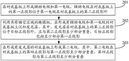
示例地,图2为本发明实施例提供的一种发光器件的制造方法的流程图,如图2所示,该发光器件的制造方法可以包括:For example, FIG. 2 is a flowchart of a method for manufacturing a light-emitting device according to an embodiment of the present invention. As shown in FIG. 2 , the method for manufacturing a light-emitting device may include:
步骤201、在衬底基板上形成辅助电极和第一电极,辅助电极在衬底基板上的第一正投影位于第一电极在衬底基板上的第二正投影外。
步骤202、利用具有镂空区域的掩膜板,在形成有辅助电极和第一电极的衬底基板上沉积发光层,其中,发光层在衬底基板上的第三正投影位于目标正投影外,且与第二正投影至少部分重叠,目标正投影包括至少部分第一正投影。
步骤203、在形成有发光层的衬底基板上形成第二电极,其中,第二电极在衬底基板上的第四正投影与目标正投影至少部分重叠,第四正投影与第三正投影至少部分重叠。
综上所述,本发明实施例提供的发光器件的制造方法中,在衬底基板上形成辅助电极和第一电极后,利用掩膜板沉积发光层,且发光层并未覆盖辅助电极。之后,再形成第二电极,以使第二电极能够直接覆盖辅助电极和发光层,从而实现第二电极电连接至辅助电极。由于该制造方法中并未使用激光,因此,发光层上并不会附着有杂质颗粒,发光器件的发光效果也不会受到杂质颗粒的影响。To sum up, in the method for manufacturing a light emitting device provided by the embodiment of the present invention, after the auxiliary electrode and the first electrode are formed on the base substrate, a mask is used to deposit the light emitting layer, and the light emitting layer does not cover the auxiliary electrode. After that, the second electrode is formed, so that the second electrode can directly cover the auxiliary electrode and the light-emitting layer, so as to realize the electrical connection of the second electrode to the auxiliary electrode. Since a laser is not used in this manufacturing method, impurity particles are not attached to the light-emitting layer, and the light-emitting effect of the light-emitting device is not affected by the impurity particles.
另外,利用掩膜板形成发光层的效率较高,因此,本发明实施例中发光器件的制造效率高于相关技术中发光器件的制造效率。In addition, the efficiency of forming the light-emitting layer by using the mask is relatively high. Therefore, the manufacturing efficiency of the light-emitting device in the embodiment of the present invention is higher than the manufacturing efficiency of the light-emitting device in the related art.
示例地,图3为本发明实施例提供的另一种发光器件的制造方法的流程图,如图3所示,该发光器件的制造方法可以包括:For example, FIG. 3 is a flowchart of another method for manufacturing a light-emitting device according to an embodiment of the present invention. As shown in FIG. 3 , the manufacturing method for the light-emitting device may include:
步骤301、在衬底基板上形成控制电路层。
该控制电路层可以包括多个绝缘层和多个导体层,且该多个绝缘层和多个导体层能够形成薄膜晶体管(或者薄膜晶体管和电容)。在步骤301之后,就可以得到如图4所示的结构,该结构包括衬底基板021,以及位于衬底基板021上的控制电路层022。The control circuit layer may include a plurality of insulating layers and a plurality of conductor layers, and the plurality of insulating layers and the plurality of conductor layers can form thin film transistors (or thin film transistors and capacitors). After
步骤302、在形成有控制电路层的衬底基板上形成辅助电极。
在步骤302中,可以采用涂覆、物理气相沉积(英文:Physical Vapor Deposition;简称:PVD)或化学气相沉积(英文:Chemical Vapor Deposition;简称:CVD)等方法在形成有控制电路层的衬底基板上形成一层导电材料,得到导电材质层。其中,PVD包括:磁控溅射或热蒸发等物理沉积方法,CVD包括离子体增强化学气相沉积法(英文: Plasma EnhancedChemical Vapor Deposition;简称:PECVD)等化学沉积方法。In
在得到导电材质层后,可以采用一次构图工艺对该导电材质层进行处理就可以得到如图5所示的辅助电极023。一次构图工艺包括:光刻胶涂覆、曝光、显影、刻蚀和光刻胶剥离。采用一次构图工艺对导电材质层进行处理包括:在导电材质层上涂覆一层光刻胶;然后采用掩膜版对光刻胶进行曝光,使光刻胶形成曝光区和非曝光区;之后采用显影工艺进行处理,使曝光区和非曝光区中一种区域的光刻胶被去除,而另一种区域的光刻胶保留;之后对导电材质层上未覆盖有光刻胶的区域进行刻蚀;刻蚀完毕后剥离导电材质层上的光刻胶即可得到辅助电极。After the conductive material layer is obtained, a patterning process may be used to process the conductive material layer to obtain the
需要说明的是,光刻胶可以为正性光刻胶或负性光刻胶。若光刻胶为正性光刻胶,则在上述显影工艺之后,曝光区的光刻胶被去除,而非曝光区的光刻胶保留;若光刻胶为负性光刻胶,则在上述显影工艺之后,非曝光区的光刻胶被去除,而曝光区的光刻胶保留。It should be noted that the photoresist may be a positive photoresist or a negative photoresist. If the photoresist is a positive photoresist, after the above-mentioned developing process, the photoresist in the exposed area is removed, but the photoresist in the non-exposed area remains; if the photoresist is a negative photoresist, After the above-mentioned developing process, the photoresist in the non-exposed area is removed, while the photoresist in the exposed area remains.
步骤303、在形成有辅助电极的衬底基板上形成第一电极,辅助电极在衬底基板上的第一正投影位于第一电极在衬底基板上的第二正投影外。
在形成辅助电极后,可以在形成有辅助电极的衬底基板上,采用涂覆、PVD或CVD等方法形成一层导电材料,得到导电材质层。在得到该导电材质层后,可以采用一次构图工艺对该导电材质层进行处理就可以得到如图6所示的第一电极024。第一电极024与控制电路层022电连接。After the auxiliary electrode is formed, a layer of conductive material may be formed on the base substrate on which the auxiliary electrode is formed by coating, PVD or CVD to obtain a conductive material layer. After the conductive material layer is obtained, a patterning process may be used to process the conductive material layer to obtain the
辅助电极023和第一电极024均可以位于控制电路层022远离衬底基板的表面。如图6所示,辅助电极023在衬底基板021上的第一正投影B1位于第一电极024在衬底基板021上的第二正投影B2外,相当于辅助电极023和第一电极024相互绝缘。Both the
需要说明的是,第一电极和辅助电极的材质可以相同也可以不同,当第一电极和辅助电极的材质相同或不同时,均可以按照步骤302和步骤303中的方式形成辅助电极和第一电极。当第一电极和辅助电极的材质相同时,还可以是不采用步骤302和步骤303的方式形成辅助电极和第一电极。比如,可以直接在形成有控制电路层的衬底基板上形成导电材质层,之后,再通过一次构图工艺对该导电材质层进行处理,即可同时得到上述辅助电极和第一电极。本发明实施例对此不作限定。It should be noted that the materials of the first electrode and the auxiliary electrode can be the same or different. When the materials of the first electrode and the auxiliary electrode are the same or different, the auxiliary electrode and the first electrode can be formed according to the methods in
步骤304、将掩膜板置于辅助电极远离衬底基板的一侧的目标位置,以使目标正投影位于目标非镂空区域在衬底基板上的正投影内,且第二正投影与镂空区域在衬底基板上的正投影存在重叠,其中,目标正投影包括至少部分第一正投影。Step 304: Place the mask at the target position on the side of the auxiliary electrode away from the base substrate, so that the target orthographic projection is located in the orthographic projection of the target non-hollow area on the base substrate, and the second orthographic projection and the hollow area The orthographic projections on the base substrate overlap, wherein the target orthographic projection includes at least part of the first orthographic projection.
本发明实施例中利用掩膜板制备发光器件,如图7所示,该掩膜板03具有镂空区域031和目标非镂空区域032。可选地,掩膜板03还可以包括除镂空区域031和目标非镂空区域032之外的辅助非镂空区域(图7中未标出)。示例地,该掩膜板03可以为精细金属掩膜板(英文:Fine Metal Mask;简称:FFM)。In the embodiment of the present invention, a mask plate is used to prepare a light-emitting device. As shown in FIG. 7 , the
在形成辅助电极023和第一电极024后,可以将掩膜板03置于辅助电极023远离衬底基板021的一侧的目标位置(如图7中掩膜板所在的位置)。此时,掩膜板03可以悬空在衬底基板021上,当然也可以是掩膜板03位于形成有辅助电极023和第一电极024的衬底基板021上。After the
当掩膜板位于目标位置时,目标正投影位于掩膜板03的目标非镂空区域032在衬底基板021上的正投影C3内,第一电极024在衬底基板021上的第二正投影B2与掩膜板03的镂空区域031在衬底基板021上的正投影C4存在重叠。图7中以目标正投影为辅助电极023在衬底基板021上的全部第一正投影B1为例,当然,目标正投影也可以仅包括部分第一正投影B1。图7中以正投影C3包围第一正投影B1,且第二正投影B2位于正投影C3外为例。可选地,第二正投影B2也可以不位于正投影C3外(比如第二正投影B2与正投影C3部分重叠)。When the mask is at the target position, the orthographic projection of the target is located in the orthographic projection C3 of the target
步骤305、从掩膜板远离衬底基板的一侧,通过掩膜板的镂空区域,向形成有辅助电极和第一电极的衬底基板上沉积发光层。
在将掩膜板置于目标位置后,如图8所示,可以从掩膜板03远离衬底基板021的一侧,通过掩膜板03的镂空区域031,向形成有辅助电极023和第一电极024的衬底基板021上沉积发光材质X,以在形成有辅助电极023和第一电极024的衬底基板021上形成发光层025。示例的,上述沉积发光材质的过程可以通过蒸镀等方式实现。After the mask is placed at the target position, as shown in FIG. 8 , from the side of the
沉积得到的发光层025的形状与掩膜板03中镂空区域031的形状相同,所以发光层025在衬底基板021上的第三正投影B3位于目标正投影(如图7中辅助电极023在衬底基板021上的第一正投影B1)之外,且第一电极024在衬底基板021上的第二正投影B2与该第三正投影B3至少部分重叠。The shape of the deposited light-emitting
并且,图8中以第三正投影B3包围第一正投影B1,且第二正投影B2位于第三正投影B3内为例。可选地,第二正投影B2也可以不位于第三正投影B3内(比如第二正投影B2与第三正投影B3部分重叠等)。可选地,第三正投影B3与第一正投影B1的间距可以大于零,此时发光层与辅助电极不接触。Moreover, in FIG. 8 , it is taken as an example that the third orthographic projection B3 surrounds the first orthographic projection B1 , and the second orthographic projection B2 is located within the third orthographic projection B3 . Optionally, the second orthographic projection B2 may not be located within the third orthographic projection B3 (for example, the second orthographic projection B2 and the third orthographic projection B3 partially overlap, etc.). Optionally, the distance between the third orthographic projection B3 and the first orthographic projection B1 may be greater than zero, and at this time, the light-emitting layer is not in contact with the auxiliary electrode.
步骤306、在形成有发光层的衬底基板上形成第二电极,其中,第二电极在衬底基板上的第四正投影与目标正投影至少部分重叠,第四正投影与第三正投影至少部分重叠。
上述第二电极可以为整面电极,覆盖衬底基板上的各个区域。此时,在形成上述发光层后,可以在形成有发光层的衬底基板上采用涂覆、PVD或CVD等方法形成一层导电材料,得到该第二电极。The above-mentioned second electrode may be a full-surface electrode, covering each region on the base substrate. At this time, after the above-mentioned light-emitting layer is formed, a layer of conductive material can be formed on the base substrate on which the light-emitting layer is formed by coating, PVD or CVD, etc., to obtain the second electrode.
如图9所示,第二电极026在衬底基板011上的第四正投影B4与目标正投影(如辅助电极023在衬底基板011上的第一正投影B1)至少部分重叠。第二电极026在衬底基板011上的第四正投影B4与发光层025在衬底基板011上的第三正投影B3至少部分重叠。可以看出,在步骤306之前形成的发光层025并未覆盖辅助电极023,在步骤306中形成的第二电极026能够直接与辅助电极023和发光层025接触,从而实现第二电极026电连接至辅助电极023和发光层025的目的。由于第二电极与辅助电极电连接,因此,辅助电极能够降低第二电极上的阻抗。As shown in FIG. 9 , the fourth orthographic projection B4 of the
需要说明的是,图9中以第一正投影B1和第三正投影B3均位于第四正投影B4内为例。可选地,第一正投影B1和第三正投影B3也可以不是均位于第四正投影B4内(比如第三正投影B3可以与第四正投影B4部分重叠等)。It should be noted that in FIG. 9 , the first orthographic projection B1 and the third orthographic projection B3 are both located within the fourth orthographic projection B4 as an example. Optionally, the first orthographic projection B1 and the third orthographic projection B3 may not both be located within the fourth orthographic projection B4 (for example, the third orthographic projection B3 may partially overlap with the fourth orthographic projection B4, etc.).
在执行完毕步骤306后,即可得到发光器件,且该发光器件中的发光层能够在第一电极上的电位和第二电极上的电位的作用下发光,第一电极上的电位可以由控制电路层提供。该第一电极、发光层和第二电极可以组成OLED或发光二极管(英文:Light EmittingDiode;简称:LED)或其他能够发光的元件,本发明实施例对此不作限定。After
需要说明的是,本发明实施例制造得到的发光器件可以为顶发光器件也可以为底发光器件,本发明实施例对此不作限定。当发光器件为顶发光器件时,第一电极遮光且第二电极透光(如第一电极的材质包括金属或石墨烯等,第二电极的材质包括为氧化铟锡或氧化铟锌等),衬底基板可以透光也可以遮光,此时发光器件中第二电极所在侧出光。当发光器件为底发光器件时,第一电极透光且第二电极遮光(如第一电极的材质包括氧化铟锡或氧化铟锌等,第二电极的材质包括为金属或石墨烯等),且衬底基板透光,此时发光器件中第一电极所在侧出光。It should be noted that, the light-emitting device manufactured in the embodiment of the present invention may be a top light-emitting device or a bottom light-emitting device, which is not limited in the embodiment of the present invention. When the light-emitting device is a top light-emitting device, the first electrode shields light and the second electrode transmits light (for example, the material of the first electrode includes metal or graphene, and the material of the second electrode includes indium tin oxide or indium zinc oxide, etc.), The base substrate can transmit light or block light. In this case, the side where the second electrode is located in the light emitting device emits light. When the light-emitting device is a bottom light-emitting device, the first electrode transmits light and the second electrode shields light (for example, the material of the first electrode includes indium tin oxide or indium zinc oxide, and the material of the second electrode includes metal or graphene, etc.), In addition, the base substrate transmits light, and at this time, the light-emitting device emits light from the side where the first electrode is located.
另外,无论发光器件为顶发光器件还是底发光器件,上述辅助电极均可以透光或遮光。比如辅助电极的材质包括金属(如铝或铜)或氧化铟锡等。In addition, no matter whether the light emitting device is a top light emitting device or a bottom light emitting device, the above-mentioned auxiliary electrode can transmit or shield light. For example, the material of the auxiliary electrode includes metal (such as aluminum or copper) or indium tin oxide.
本发明实施例以制造得到的发光器件如图9所示为例,可选地,发光器件也可以与图9所示的结构不同。比如,制造得到的发光器件也可以不包括控制电路层,此时,无需执行步骤201,且在步骤202中可以直接在衬底基板上形成辅助电极。In this embodiment of the present invention, the manufactured light-emitting device is shown in FIG. 9 as an example. Optionally, the structure of the light-emitting device may also be different from that shown in FIG. 9 . For example, the manufactured light-emitting device may not include a control circuit layer. In this case,
综上所述,本发明实施例提供的发光器件的制造方法中,在衬底基板上形成辅助电极和第一电极后,利用掩膜板沉积发光层,且发光层并未覆盖辅助电极。之后,再形成第二电极,以使第二电极能够直接覆盖辅助电极和发光层,从而实现第二电极电连接至辅助电极。由于该制造方法中并未使用激光,因此,发光层上并不会附着有杂质颗粒,发光器件的发光效果也不会受到杂质颗粒的影响。To sum up, in the method for manufacturing a light emitting device provided by the embodiment of the present invention, after the auxiliary electrode and the first electrode are formed on the base substrate, a mask is used to deposit the light emitting layer, and the light emitting layer does not cover the auxiliary electrode. After that, the second electrode is formed, so that the second electrode can directly cover the auxiliary electrode and the light-emitting layer, so as to realize the electrical connection of the second electrode to the auxiliary electrode. Since a laser is not used in this manufacturing method, impurity particles are not attached to the light-emitting layer, and the light-emitting effect of the light-emitting device is not affected by the impurity particles.
另外,利用掩膜板形成发光层的效率较高,因此,本发明实施例中发光器件的制造效率高于相关技术中发光器件的制造效率。In addition, the efficiency of forming the light-emitting layer by using the mask is relatively high. Therefore, the manufacturing efficiency of the light-emitting device in the embodiment of the present invention is higher than the manufacturing efficiency of the light-emitting device in the related art.
本发明实施例提供了一种发光器件,该发光器件可以由本发明实施例提供的发光器件的制造方法(如图2或图3所示的方法)制成。The embodiment of the present invention provides a light-emitting device, and the light-emitting device can be manufactured by the method for manufacturing a light-emitting device provided by the embodiment of the present invention (the method shown in FIG. 2 or FIG. 3 ).
如图9所示,该发光器件02包括:衬底基板021、辅助电极023、第一电极024、发光层025和第二电极026;第一电极024与辅助电极023位于衬底基板021上,且辅助电极023在衬底基板021上的第一正投影B1位于第一电极024在衬底基板021上的第二正投影B2外。As shown in FIG. 9 , the light-emitting
发光层025位于辅助电极023远离衬底基板021的一侧,且发光层025在衬底基板021上的第三正投影B3位于目标正投影之外,第二正投影B2与第三正投影B3至少部分重叠。该目标正投影包括至少部分第一正投影B1,图9中以目标正投影包括全部的第一正投影B1为例。The light-emitting
第二电极026位于发光层025远离衬底基板021的一侧,且第二电极026在衬底基板021上的第四正投影B4与目标正投影(如上述第一正投影B1)至少部分重叠,第四正投影B4与第三正投影B3至少部分重叠。The
可选地,请继续参考图9,该发光器件02还可以包括控制电路层022,控制电路层022位于衬底基板021上,辅助电极023和第一电极024位于形成有控制电路层022的衬底基板021上。第一电极024与控制电路层022电连接。当然,发光器件02也可以不包括控制电路层022,本发明实施例对此不作限定。Optionally, please continue to refer to FIG. 9 , the light-emitting
本发明实施例还提供了一种掩膜板,该掩膜板可以用于制备本发明实施例提供的发光器件(如图9所示的发光器件)。如图7所示,该掩膜板03具有镂空区域031和目标非镂空区域032。The embodiment of the present invention also provides a mask, which can be used to prepare the light-emitting device provided by the embodiment of the present invention (the light-emitting device shown in FIG. 9 ). As shown in FIG. 7 , the
在掩膜板03位于辅助电极023远离衬底基板021的一侧的目标位置(如图7中掩膜板所在的位置)时,目标正投影(如辅助电极023在衬底基板021上的第一正投影B1)位于掩膜板03的目标非镂空区域032在衬底基板021上的正投影C3内,第一电极024在衬底基板021上的第二正投影B2与掩膜板03的镂空区域031在衬底基板021上的正投影C4存在重叠。When the
本发明实施例还提供了一种显示基板,该显示基板可以包括:本发明实施例提供的发光器件(如图9所示的发光器件)。The embodiment of the present invention further provides a display substrate, and the display substrate may include: the light-emitting device provided by the embodiment of the present invention (the light-emitting device shown in FIG. 9 ).
图10为本发明实施例提供的一种显示装置的结构示意图,如图10所示,该显示装置04可以包括:本发明实施例提供的显示基板,该显示基板包括本发明实施例提供的发光器件。图10中以发光器件为图9所示的发光器件为例。FIG. 10 is a schematic structural diagram of a display device provided by an embodiment of the present invention. As shown in FIG. 10 , the
可选地,显示装置04还可以包括盖板05。盖板05可以与发光器件02中的衬底基板021相对设置,发光器件02中除衬底基板021之外的其他结构均位于衬底基板021和盖板05之间。Optionally, the
可选地,显示装置04还可以包括:位于盖板05朝向衬底基板021一侧的彩膜06和黑矩阵07。此时,发光器件02发出的光可以为白光。需要说明的是,当显示装置04不包括彩膜06时,发光器件02发出的光可以为白光或者彩色光。Optionally, the
可选地,显示装置还可以包括:位于彩膜06朝向衬底基板021一侧的上层覆盖层08。可选地,显示装置还可以包括:位于上层覆盖层08和发光器件01之间的填充层09、支撑柱10和封框胶(图10中未示出)。Optionally, the display device may further include: an
在制造图10所示的显示装置时,可以采用本发明实施例提供的发光器件的制备方法制备发光元件,进而得到显示基板。还可以在盖板上形成彩膜、黑矩阵和上层覆盖层。之后,在显示基板中第二电极所在侧形成填充层、支撑柱和封框胶,再将形成有彩膜、黑矩阵和上层覆盖层的盖板与显示基板对盒即可。When manufacturing the display device shown in FIG. 10 , a light-emitting element can be prepared by using the method for preparing a light-emitting device provided in the embodiment of the present invention, and then a display substrate can be obtained. A color filter, a black matrix and an upper cover layer can also be formed on the cover plate. After that, a filling layer, a support column and a sealant are formed on the side where the second electrode is located in the display substrate, and then the cover plate on which the color filter, the black matrix and the upper cover layer are formed is assembled with the display substrate.
另外,本发明实施例提供的显示装置可以为:显示面板(如OLED显示面板或LED显示面板)、电子纸、手机、平板电脑、电视机、显示器、笔记本电脑、数码相框、导航仪等任何具有显示功能的产品或部件。In addition, the display device provided by the embodiment of the present invention may be: a display panel (such as an OLED display panel or an LED display panel), an electronic paper, a mobile phone, a tablet computer, a TV, a monitor, a notebook computer, a digital photo frame, a navigator, etc. A product or part that displays functionality.
本发明实施例提供的显示装置可以为大尺寸(如大于30~40英寸)的显示装置,或小尺寸(如小于或等于30英寸)的显示装置。The display device provided by the embodiment of the present invention may be a display device with a large size (eg, greater than 30 to 40 inches), or a display device with a small size (eg, less than or equal to 30 inches).
需要指出的是,在附图中,为了图示的清晰可能夸大了层和区域的尺寸。而且可以理解,当元件或层被称为在另一元件或层“上”时,它可以直接在其他元件上,或者可以存在中间的层。另外,可以理解,当元件或层被称为在另一元件或层“下”时,它可以直接在其他元件下,或者可以存在一个以上的中间的层或元件。另外,还可以理解,当层或元件被称为在两层或两个元件“之间”时,它可以为两层或两个元件之间唯一的层,或还可以存在一个以上的中间层或元件。通篇相似的参考标记指示相似的元件。It should be noted that, in the drawings, the sizes of layers and regions may be exaggerated for clarity of illustration. It will also be understood that when an element or layer is referred to as being "on" another element or layer, it can be directly on the other element or intervening layers may be present. In addition, it will be understood that when an element or layer is referred to as being "under" another element or layer, it can be directly under the other element, or more than one intervening layer or element may be present. In addition, it will also be understood that when a layer or element is referred to as being 'between' two layers or elements, it can be the only layer between the two layers or elements, or more than one intervening layer may also be present or element. Like reference numerals indicate like elements throughout.
在本公开中,术语“第一”、“第二”、“第三”和“第四”仅用于描述目的,而不能理解为指示或暗示相对重要性。术语“多个”指两个或两个以上,除非另有明确的限定。In this disclosure, the terms "first," "second," "third," and "fourth" are used for descriptive purposes only, and should not be construed to indicate or imply relative importance. The term "plurality" refers to two or more, unless expressly limited otherwise.
本发明中术语“和/或”,仅仅是一种描述关联对象的关联关系,表示可以存在三种关系,例如,A和/或B,可以表示:单独存在A,同时存在A和B,单独存在B这三种情况。另外,本文中字符“/”,一般表示前后关联对象是一种“或”的关系。The term "and/or" in the present invention is only an association relationship to describe associated objects, indicating that there can be three kinds of relationships, for example, A and/or B, it can mean that A exists alone, A and B exist at the same time, independently There are three cases of B. In addition, the character "/" in this document generally indicates that the related objects are an "or" relationship.
需要说明的是,本发明实施例提供的方法实施例能够与相应的发光模组实施例相互参考,本发明实施例对此不做限定。本发明实施例提供的方法实施例步骤的先后顺序能够进行适当调整,步骤也能够根据情况进行相应增减,任何熟悉本技术领域的技术人员在本发明揭露的技术范围内,可轻易想到变化的方法,都应涵盖在本发明的保护范围之内,因此不再赘述。It should be noted that, the method embodiments provided in the embodiments of the present invention can be cross-referenced with the corresponding light-emitting module embodiments, which are not limited in the embodiments of the present invention. The sequence of the steps of the method embodiments provided by the embodiments of the present invention can be appropriately adjusted, and the steps can also be increased or decreased according to the situation. All methods should be covered within the protection scope of the present invention, and therefore will not be repeated here.
以上所述仅为本申请的可选实施例,并不用以限制本申请,凡在本申请的精神和原则之内,所作的任何修改、等同替换、改进等,均应包含在本申请的保护范围之内。The above descriptions are only optional embodiments of the present application, and are not intended to limit the present application. Any modifications, equivalent replacements, improvements, etc. made within the spirit and principles of the present application shall be included in the protection of the present application. within the range.
Claims (9)
Priority Applications (3)
| Application Number | Priority Date | Filing Date | Title |
|---|---|---|---|
| CN201910425411.8A CN110148615B (en) | 2019-05-21 | 2019-05-21 | Light-emitting device and manufacturing method thereof, mask plate, display substrate and device |
| PCT/CN2020/090148 WO2020233485A1 (en) | 2019-05-21 | 2020-05-14 | Light-emitting component, manufacturing method therefor, mask, and display device |
| US17/271,637 US11723261B2 (en) | 2019-05-21 | 2020-05-14 | Light-emitting component, manufacturing method therefor, mask, and display device |
Applications Claiming Priority (1)
| Application Number | Priority Date | Filing Date | Title |
|---|---|---|---|
| CN201910425411.8A CN110148615B (en) | 2019-05-21 | 2019-05-21 | Light-emitting device and manufacturing method thereof, mask plate, display substrate and device |
Publications (2)
| Publication Number | Publication Date |
|---|---|
| CN110148615A CN110148615A (en) | 2019-08-20 |
| CN110148615B true CN110148615B (en) | 2022-09-23 |
Family
ID=67592593
Family Applications (1)
| Application Number | Title | Priority Date | Filing Date |
|---|---|---|---|
| CN201910425411.8A Active CN110148615B (en) | 2019-05-21 | 2019-05-21 | Light-emitting device and manufacturing method thereof, mask plate, display substrate and device |
Country Status (3)
| Country | Link |
|---|---|
| US (1) | US11723261B2 (en) |
| CN (1) | CN110148615B (en) |
| WO (1) | WO2020233485A1 (en) |
Families Citing this family (3)
| Publication number | Priority date | Publication date | Assignee | Title |
|---|---|---|---|---|
| CN110148615B (en) * | 2019-05-21 | 2022-09-23 | 京东方科技集团股份有限公司 | Light-emitting device and manufacturing method thereof, mask plate, display substrate and device |
| CN110942041B (en) * | 2019-11-29 | 2023-11-28 | 京东方科技集团股份有限公司 | Display substrate, manufacturing method and display device thereof |
| CN115064568B (en) * | 2022-06-14 | 2025-09-26 | 京东方科技集团股份有限公司 | Display panel, manufacturing method thereof, and display device |
Citations (2)
| Publication number | Priority date | Publication date | Assignee | Title |
|---|---|---|---|---|
| CN103882374A (en) * | 2014-03-03 | 2014-06-25 | 京东方科技集团股份有限公司 | Mask, organic layer machining method and display substrate preparation method |
| CN109713162A (en) * | 2018-12-27 | 2019-05-03 | 武汉天马微电子有限公司 | Display panel and display device |
Family Cites Families (8)
| Publication number | Priority date | Publication date | Assignee | Title |
|---|---|---|---|---|
| KR101254748B1 (en) * | 2009-05-06 | 2013-04-15 | 엘지디스플레이 주식회사 | Organic Light Emitting Display Device and Manufacturing Method of the same |
| KR102069193B1 (en) * | 2013-07-22 | 2020-01-23 | 삼성디스플레이 주식회사 | Organic light emitting display apparatus and method for manufacturing the same |
| CN104659063A (en) * | 2014-12-30 | 2015-05-27 | 京东方科技集团股份有限公司 | Display substrate, manufacture method thereof, display panel and mask plate |
| KR102614598B1 (en) * | 2016-06-27 | 2023-12-18 | 삼성디스플레이 주식회사 | Organic light emitting display |
| CN108878673A (en) * | 2017-05-10 | 2018-11-23 | 京东方科技集团股份有限公司 | Display base plate and preparation method thereof, display device |
| US10411188B2 (en) | 2017-09-12 | 2019-09-10 | Shenzhen China Star Optoelectronics Semiconductor Display Technology Co., Ltd. | Mask plate for vapor deposition of organic light-emitting diode (OLED) devices and OLED device thereof |
| CN107604306A (en) * | 2017-09-12 | 2018-01-19 | 深圳市华星光电半导体显示技术有限公司 | For the mask plate of OLED evaporation and its OLED of manufacture |
| CN110148615B (en) * | 2019-05-21 | 2022-09-23 | 京东方科技集团股份有限公司 | Light-emitting device and manufacturing method thereof, mask plate, display substrate and device |
-
2019
- 2019-05-21 CN CN201910425411.8A patent/CN110148615B/en active Active
-
2020
- 2020-05-14 WO PCT/CN2020/090148 patent/WO2020233485A1/en not_active Ceased
- 2020-05-14 US US17/271,637 patent/US11723261B2/en active Active
Patent Citations (2)
| Publication number | Priority date | Publication date | Assignee | Title |
|---|---|---|---|---|
| CN103882374A (en) * | 2014-03-03 | 2014-06-25 | 京东方科技集团股份有限公司 | Mask, organic layer machining method and display substrate preparation method |
| CN109713162A (en) * | 2018-12-27 | 2019-05-03 | 武汉天马微电子有限公司 | Display panel and display device |
Also Published As
| Publication number | Publication date |
|---|---|
| WO2020233485A1 (en) | 2020-11-26 |
| CN110148615A (en) | 2019-08-20 |
| US11723261B2 (en) | 2023-08-08 |
| US20210184126A1 (en) | 2021-06-17 |
Similar Documents
| Publication | Publication Date | Title |
|---|---|---|
| CN111864116B (en) | Display substrate, preparation method thereof and display device | |
| CN110112201B (en) | Display substrate, manufacturing method thereof and display device | |
| CN110943112B (en) | Array substrate and preparation method thereof, and display panel | |
| WO2019165826A1 (en) | Touch display substrate, fabrication method thereof, and display apparatus | |
| CN116916695B (en) | Display panel and display device | |
| CN108649060B (en) | OLED device and preparation method thereof, and display device | |
| CN111430428B (en) | Flexible display panel, manufacturing method thereof and display device | |
| CN110148615B (en) | Light-emitting device and manufacturing method thereof, mask plate, display substrate and device | |
| CN111584608A (en) | OLED display substrate, manufacturing method thereof, display panel and display device | |
| CN105742299B (en) | A kind of pixel unit and preparation method thereof, array substrate and display device | |
| CN112068732A (en) | A display panel and display device | |
| CN104867962A (en) | OLED array substrate, production method thereof, OLED display device | |
| CN110212091A (en) | Mask plate, oled display substrate and preparation method thereof, display device is deposited | |
| WO2019010953A1 (en) | Array substrate and preparation method therefor, display panel, and display device | |
| CN110289366A (en) | Cover plate structure and manufacturing method thereof, display panel, display device | |
| CN101740726B (en) | Organic electroluminescent device and manufacturing method thereof | |
| CN116322180A (en) | Display panel, display device and preparation method of display panel | |
| EP3506379B1 (en) | Oled device and manufacturing method therefor, display panel, and display apparatus | |
| CN108062181A (en) | Substrate, manufacturing method thereof, and electronic device | |
| CN105118834B (en) | Array substrate and preparation method thereof, display panel, display device | |
| CN111326565B (en) | Display panel, manufacturing method thereof and display device | |
| JP7267744B2 (en) | Touch panel, manufacturing method thereof, and display device | |
| CN120302833A (en) | Display panel, method for manufacturing display panel, and electronic device | |
| WO2022104937A1 (en) | Manufacturing method for oled panel, and oled panel | |
| CN119907572A (en) | Display panel, display device, and method for manufacturing display panel |
Legal Events
| Date | Code | Title | Description |
|---|---|---|---|
| PB01 | Publication | ||
| PB01 | Publication | ||
| SE01 | Entry into force of request for substantive examination | ||
| SE01 | Entry into force of request for substantive examination | ||
| GR01 | Patent grant | ||
| GR01 | Patent grant |