CN110021237B - A method of transferring MICRO LED chips from wafer to panel - Google Patents
A method of transferring MICRO LED chips from wafer to panel Download PDFInfo
- Publication number
- CN110021237B CN110021237B CN201811080486.9A CN201811080486A CN110021237B CN 110021237 B CN110021237 B CN 110021237B CN 201811080486 A CN201811080486 A CN 201811080486A CN 110021237 B CN110021237 B CN 110021237B
- Authority
- CN
- China
- Prior art keywords
- micro led
- unit
- led chip
- panel
- wafer
- Prior art date
- Legal status (The legal status is an assumption and is not a legal conclusion. Google has not performed a legal analysis and makes no representation as to the accuracy of the status listed.)
- Active
Links
Images


Classifications
-
- G—PHYSICS
- G09—EDUCATION; CRYPTOGRAPHY; DISPLAY; ADVERTISING; SEALS
- G09F—DISPLAYING; ADVERTISING; SIGNS; LABELS OR NAME-PLATES; SEALS
- G09F9/00—Indicating arrangements for variable information in which the information is built-up on a support by selection or combination of individual elements
- G09F9/30—Indicating arrangements for variable information in which the information is built-up on a support by selection or combination of individual elements in which the desired character or characters are formed by combining individual elements
- G09F9/33—Indicating arrangements for variable information in which the information is built-up on a support by selection or combination of individual elements in which the desired character or characters are formed by combining individual elements being semiconductor devices, e.g. diodes
-
- H10P54/00—
Landscapes
- Physics & Mathematics (AREA)
- General Physics & Mathematics (AREA)
- Engineering & Computer Science (AREA)
- Theoretical Computer Science (AREA)
- Led Device Packages (AREA)
- Led Devices (AREA)
Abstract
本发明公开了一种MICRO LED芯片从晶圆转出转入面板的方法,晶圆上MICRO LED芯片包括第一单元、第二单元,MICRO LED芯片从晶圆转出转入面板包括MICRO LED芯片的两次转移:第一次转移、第二次转移。本方法转移MICRO LED芯片不但简单,并且提高了生产过程中晶圆上MICRO LED芯片利用率,使MICRO LED芯片能与面板上的绑定点精准定位固定。
The invention discloses a method for transferring a MICRO LED chip from a wafer to a panel. The MICRO LED chip on the wafer includes a first unit and a second unit, and the MICRO LED chip transferred from the wafer to the panel includes the MICRO LED chip two transfers: the first transfer, the second transfer. The method is not only simple to transfer the MICRO LED chip, but also improves the utilization rate of the MICRO LED chip on the wafer during the production process, so that the MICRO LED chip can be accurately positioned and fixed with the binding point on the panel.
Description
技术领域technical field
本发明涉及MICRO LED芯片技术。更具体地说,本发明涉及MICRO LED芯片从晶圆转出转入面板的方法。The present invention relates to MICRO LED chip technology. More specifically, the present invention relates to a method for transferring MICRO LED chips from wafers to panels.
背景技术Background technique
在2018年1月份的CES展会上,三星推出了一款146英寸的巨型电视,这款电视为三星在对Micro LED长期研究后,第一款使用Micro LED技术的电视。Micro LED电视相对其它技术的电视,其亮度、对比度、色彩饱和度等各方面都有了突出的进步,因Micro LED的良好特性,其在显示技术领域的应用得到了广泛的推广,如智能手表、智能手机、电视显示器、平板电脑等等,经行业预估,Micro LED技术在大尺寸显示器市场的应用到2025年将占整个市场的68%以上,预估价值达19.8亿美元。此项预估值并非空穴来风,早在去年1月份索尼公司就在美国消费电子展上展示了一块Micro LED技术无缝拼接的大型显示屏,同年3月,谷歌公司申请了一项用Micro LED技术的显示屏制备的新款谷歌眼镜的技术专利,这项专利布局充分显示谷歌公司对该技术的热衷。At the CES show in January 2018, Samsung launched a 146-inch giant TV. This TV is Samsung's first TV to use Micro LED technology after long-term research on Micro LED. Compared with TVs of other technologies, Micro LED TV has made outstanding progress in brightness, contrast, color saturation and other aspects. Due to the good characteristics of Micro LED, its application in the field of display technology has been widely promoted, such as smart watches. , smartphones, TV monitors, tablet computers, etc. According to industry estimates, the application of Micro LED technology in the large-size display market will account for more than 68% of the entire market by 2025, with an estimated value of US$1.98 billion. This estimate is not groundless. As early as last January, Sony showed a large-scale display with Micro LED technology seamless splicing at the Consumer Electronics Show in the United States. In March of the same year, Google applied for a Micro LED technology. The technology patent of the new Google Glass made of the display screen, this patent layout fully shows Google's enthusiasm for the technology.
目前,随着国际巨头企业如:苹果、三星、索尼等在Micro LED技术方面急速布局,国内各大LED厂商也在Micro LED技术领域进行紧锣密鼓,充分显示了Micro LED技术的应用将成分这一行业的必然趋势,但根据行业内专家多年研究经验发现,由于Micro LED技术在显示技术的应用需要各方面技术的整合,如精密机械、半导体制程、测试、检修等等,都不能再仅仅停留于现有的光电技术领域,而Micro LED技术本身又存在几个关键问题:成本高、良率太低、批量生产困难等等。若不能切实有效地解决这些问题,Micro LED技术的应用推广将举步维艰,很难被广泛应用于显示器技术领域,阻碍了Micro LED显示器的商品化进程。At present, with the rapid deployment of international giants such as Apple, Samsung, Sony, etc. in Micro LED technology, major domestic LED manufacturers are also in the field of Micro LED technology, which fully shows that the application of Micro LED technology will make up this industry. However, according to the research experience of experts in the industry for many years, it is found that the application of Micro LED technology in display technology requires the integration of various technologies, such as precision machinery, semiconductor process, testing, maintenance, etc. In some optoelectronic technology fields, Micro LED technology itself has several key problems: high cost, low yield, difficulty in mass production, etc. If these problems cannot be solved effectively, the application and promotion of Micro LED technology will be difficult, and it will be difficult to be widely used in the field of display technology, which hinders the commercialization of Micro LED displays.
发明内容SUMMARY OF THE INVENTION
本发明的目的是提供一种MICRO LED芯片从晶圆转出转入面板的方法,用于提高MICRO LED芯片在显示技术中的良率,使MICRO LED芯片能与面板上的绑定点精准定位固定,并且提高了生产过程中晶圆上MICRO LED芯片利用率,降低生产成本,解决批量生产困难等系列问题。The purpose of the present invention is to provide a method for transferring MICRO LED chips from a wafer to a panel, which is used to improve the yield of the MICRO LED chips in display technology, so that the MICRO LED chips can be precisely positioned with the binding points on the panel It also improves the utilization rate of MICRO LED chips on the wafer in the production process, reduces production costs, and solves a series of problems such as difficulty in mass production.
为了实现根据本发明的目的和其它优点,本发明提供了一种 MICRO LED芯片从晶圆转出转入面板的方法,其中所述的晶圆上MICRO LED芯片包括第一单元、第二单元,所述的MICRO LED芯片从晶圆转出转入面板包括MICRO LED芯片的两次转移:第一次转移、第二次转移:In order to achieve the object and other advantages according to the present invention, the present invention provides a method for transferring MICRO LED chips from a wafer to a panel, wherein the on-wafer MICRO LED chips include a first unit and a second unit, The transfer of the MICRO LED chip from the wafer to the panel includes two transfers of the MICRO LED chip: the first transfer and the second transfer:
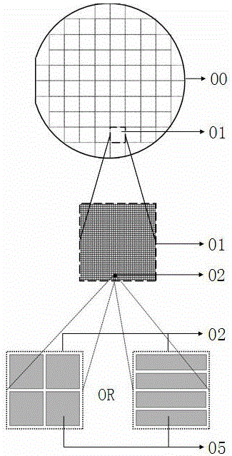
第一单元、第二单元均为MICRO LED芯片集,第二单元为第一单元的子单元,第一单元中包括第二单元的数量≥2,第二单元中包含的MICRO LED芯片的数量≥2;第二单元可以是个虚拟单元,并不一定非要标识出第二单元,为了与面板上的薄膜电晶体位置匹配,在第一单元上每次同时转移出间距相等所对应位置的MICRO LED芯片,如图1所示,第一单元上第二单元的区域面积划分一般根据面板上的薄膜电晶体所占位置来定。The first unit and the second unit are both MICRO LED chip sets, the second unit is a sub-unit of the first unit, the number of second units included in the first unit is ≥ 2, and the number of MICRO LED chips included in the second unit is greater than or equal to 2 2; The second unit can be a virtual unit, and it is not necessary to identify the second unit. In order to match the position of the thin film transistor on the panel, the MICRO LEDs at the corresponding positions with equal spacing are simultaneously transferred on the first unit each time. For the chip, as shown in FIG. 1 , the area division of the second unit on the first unit is generally determined according to the position occupied by the thin film transistor on the panel.
在晶圆进行定量划分MICRO LED芯片第一单元区域,以第一单元为单元从晶圆上第一次转移MICRO LED芯片,转出的第一单元MICRO LED芯片集以第二单元为单位进行MICRO LED芯片的第二次转移,以第一单元中每个第二单元上每次一颗MICRO LED芯片转移至面板,MICRO LED芯片与面板上的薄膜电晶体相固定,同一次转移时各第二单元上转出的MICRO LED芯片位于各第二单元的相同位置,如同是1号位置,或同是2号位置等。Quantitatively divide the first unit area of the MICRO LED chip on the wafer, transfer the MICRO LED chip from the wafer for the first time in the first unit, and transfer the first unit MICRO LED chip set to the second unit. For the second transfer of LED chips, one MICRO LED chip on each second unit in the first unit is transferred to the panel at a time, and the MICRO LED chips are fixed with the thin film transistor on the panel. The MICRO LED chips transferred out of the unit are located in the same position of each second unit, such as the No. 1 position, or the same No. 2 position.
本发明所述的MICRO LED芯片从晶圆转出转入面板的方法,其中所述的MICRO LED芯片从晶圆转出转入薄膜电晶体,其中进一步包括临时基板,用于临时固定MICRO LED芯片,临时基板上与每个薄膜电晶体相同面积区域内固定一颗MICRO LED芯片;并且其中的第二次转移包括两步,分别为第二次第一步转移、第二次第二步转移,其中第二次第一步转移,以第一单元中每个第二单元上每次一颗MICRO LED芯片转移至临时基板,MICRO LED芯片第二次第一步转移时同一次转移时各第二单元上转出的MICRO LED芯片位于各第二单元的相同位置;第二次第二步为从临时基板上一次把MICRO LED芯片向面板转移,使MICROLED芯片与面板上的薄膜电晶体相固定。The method for transferring the MICRO LED chip from the wafer to the panel according to the present invention, wherein the MICRO LED chip is transferred from the wafer to the thin film transistor, which further includes a temporary substrate for temporarily fixing the MICRO LED chip , a MICRO LED chip is fixed on the temporary substrate in the same area as each thin film transistor; and the second transfer includes two steps, respectively the second first step transfer and the second second step transfer, wherein the first transfer The second first-step transfer, one MICRO LED chip on each second unit in the first unit is transferred to the temporary substrate at a time, and the MICRO LED chips transferred from each second unit during the second first-step transfer of the MICRO LED chips are transferred at the same time. The LED chips are located in the same position of each second unit; the second step is to transfer the MICRO LED chips from the temporary substrate to the panel once, so that the MICROLED chips are fixed with the thin film transistors on the panel.
本发明所述的MICRO LED芯片从晶圆转出转入面板的方法,其中所述第二次第一步转移,包括MICRO LED芯片转移至临时基板后再次或多次MICRO LED芯片扩距转移;MICROLED芯片扩距转移包括:把临时基板上MICRO LED芯片按芯片集分单元,以每个单元上每次一颗MICRO LED芯片转移另一临时基板,MICRO LED芯片转移过程中同一次转移时各单元上转出的MICRO LED芯片位于各单元的相同位置。The method for transferring MICRO LED chips from a wafer to a panel according to the present invention, wherein the second first-step transfer includes the transfer of the MICRO LED chips to the temporary substrate again or more times after the transfer of the MICRO LED chips; The distance-expanding transfer includes: dividing the MICRO LED chips on the temporary substrate into units according to the chip set, and transferring one MICRO LED chip on each unit to another temporary substrate at a time. The outgoing MICRO LED chips are located in the same position of each unit.
本发明所述的MICRO LED芯片从晶圆转出转入面板的方法,其中所述的晶圆上第一单元的MICRO LED芯片集为包含两个或两个以上第二单元的MICRO LED芯片集,第一单元形状选自:圆形、菱形、正方形、长方形、三角形。The method for transferring MICRO LED chips from a wafer to a panel according to the present invention, wherein the MICRO LED chip set of the first unit on the wafer is a MICRO LED chip set comprising two or more second units , the first unit shape is selected from: circle, rhombus, square, rectangle, triangle.
本发明所述的MICRO LED芯片从晶圆转出转入面板的方法,其中所述的第一单元形状选自:正方形或长方形。In the method for transferring a MICRO LED chip from a wafer to a panel according to the present invention, the shape of the first unit is selected from: square or rectangle.
本发明所述的MICRO LED芯片从晶圆转出转入面板的方法,其中所述的MICRO LED芯片第二单元所占的面积区域≤一个薄膜电晶体所占的面积区域相等,形状相同,一个第二单元中包含的MICRO LED芯片的数量≤9。In the method for transferring a MICRO LED chip from a wafer to a panel according to the present invention, the area occupied by the second unit of the MICRO LED chip is equal to or less than the area occupied by a thin film transistor, with the same shape, and one The number of MICRO LED chips contained in the second unit is ≤9.
本发明所述的MICRO LED芯片从晶圆转出转入面板的方法,其中所述的第二次转移,利用激光选择性定位剥离技术以第一单元中每个第二单元上每次一颗MICRO LED芯片剥离后,转移固定至面板或临时基板。In the method for transferring MICRO LED chips from a wafer to a panel according to the present invention, in the second transfer, laser selective positioning and peeling technology is used to remove one chip at a time on each second unit in the first unit. After the MICRO LED chip is peeled off, it is transferred to a panel or temporary substrate.
本发明所述的MICRO LED芯片从晶圆转出转入面板的方法,其中所述的MICRO LED芯片在晶圆上第一次转移前完成制备。The method for transferring MICRO LED chips from a wafer to a panel according to the present invention, wherein the MICRO LED chips are prepared before the first transfer on the wafer.
本发明所述的MICRO LED芯片从晶圆转出转入面板的方法,其中所述的面板为透明基板,优选透明的玻璃基板。The method for transferring MICRO LED chips from a wafer to a panel according to the present invention, wherein the panel is a transparent substrate, preferably a transparent glass substrate.
本发明所述的MICRO LED芯片从晶圆转出转入面板的方法,其中所述的MICRO LED芯片通过MICRO LED芯片上的P电极与薄膜电晶体上的汲极点绑定固定。The method for transferring the MICRO LED chip from the wafer to the panel according to the present invention, wherein the MICRO LED chip is bound and fixed by the P electrode on the MICRO LED chip and the drain point on the thin film transistor.
本发明所述的MICRO LED芯片从晶圆转出转入面板的方法,其中所述的MICRO LED芯片通过MICRO LED芯片上的N电极与薄膜电晶体上的源极点绑定固定。The method for transferring a MICRO LED chip from a wafer to a panel according to the present invention, wherein the MICRO LED chip is bound and fixed by the N electrode on the MICRO LED chip and the source point on the thin film transistor.
本发明所述的MICRO LED芯片从晶圆转出转入面板的方法,其特征在于,根据MICRO LED芯片在临时基板转移的次数,所述的MICRO LED芯片通过MICRO LED芯片上的N电极与薄膜电晶体上的源极点绑定固定或MICRO LED芯片通过MICRO LED芯片上的P电极与薄膜电晶体上的汲极点绑定固定。The method of transferring the MICRO LED chip from the wafer to the panel according to the present invention is characterized in that, according to the transfer times of the MICRO LED chip on the temporary substrate, the MICRO LED chip passes through the N electrode and the thin film on the MICRO LED chip. The source point on the transistor is bound and fixed or the MICRO LED chip is bound and fixed with the drain point on the thin film transistor through the P electrode on the MICRO LED chip.
本发明至少包括以下有益效果:The present invention includes at least the following beneficial effects:
通过本发明能使MICRO LED芯片更好地转移向薄膜电晶体,并且使MICRO LED芯片有效利用,因晶圆上MICRO LED芯片间距与面板上所要求固定的MICRO LED芯片的间距是不同的,一般面板上所要求固定的MICRO LED芯片的间距≥2晶圆上MICRO LED芯片间距,若不使用本发明方法,晶圆上MICRO LED芯片至少有3/4将要被浪费,不能得到有效的利用。另一方面我们MICRO LED芯片一般主要用于手机显示屏的使用,即便最高分辨率,面板上所要固定的MICRO LED芯片间距与晶圆上MICRO LED芯片间距相同,但因为应用于手机显示屏需要红、绿、蓝三色MICRO LED芯片混合,所以对于同一晶圆上的MICRO LED芯片间距只能是面板上所要求固定的同色MICRO LED芯片的间距1/3。Through the invention, the MICRO LED chips can be better transferred to the thin film transistor, and the MICRO LED chips can be used effectively. Because the spacing between the MICRO LED chips on the wafer and the fixed MICRO LED chips on the panel is different, generally The required fixed spacing of MICRO LED chips on the panel is greater than or equal to 2 spacing of the MICRO LED chips on the wafer. If the method of the present invention is not used, at least 3/4 of the MICRO LED chips on the wafer will be wasted and cannot be effectively utilized. On the other hand, our MICRO LED chips are generally mainly used for the use of mobile phone displays. Even with the highest resolution, the MICRO LED chip spacing to be fixed on the panel is the same as the MICRO LED chip spacing on the wafer. , green and blue MICRO LED chips are mixed, so the spacing between MICRO LED chips on the same wafer can only be 1/3 of the same color MICRO LED chip spacing required to be fixed on the panel.
本发明通过多次转移可以扩大MICRO LED芯片之间的距离,并且可以有效利用,不浪费面积,可以把不同波长的MICRO LED芯片进行混合、参杂固定于面板,提高MICRO LED芯片光效的饱和度,做成全彩RGB,可以把红光、蓝光、绿光芯片混合、固定到面板上;另一方面使MICRO LED芯片从晶圆至面板的转移时,MICRO LED芯片电极与面板上绑定点更为精准匹配,在本发明中晶圆上的各MICRO LED芯片之间相对零位移地转移至面板。The invention can expand the distance between the MICRO LED chips through multiple transfers, and can effectively use the MICRO LED chips without wasting area. The MICRO LED chips of different wavelengths can be mixed, mixed and fixed on the panel, and the saturation of the light efficiency of the MICRO LED chips can be improved. It can be made into full-color RGB, and red, blue, and green chips can be mixed and fixed on the panel; on the other hand, when the MICRO LED chip is transferred from the wafer to the panel, the MICRO LED chip electrodes are bound to the panel. The points are more precisely matched, and in the present invention, the MICRO LED chips on the wafer are transferred to the panel with relative zero displacement.
本发明的发明人在对MICRO LED芯片制备应用的工艺研究的过程中发现,利用本发明的这种MICRO LED芯片从晶圆转出转入面板的方法,有效提高了效率及良率,在晶圆上制备完MICRO LED芯片,不需要进行单颗芯片的剥离,只需按芯片集,如本发明中定义的第一单元,按第一单元量整体从晶圆上取出MICRO LED芯片,在再第一单元上分第二单元,以每次每个第二单元上相同位置一颗MICRO LED芯片绑定至面板,并利用激光使该MICRO LED芯片从第一单元上剥离。方法简单,易于用于批量MICRO LED芯片转移。The inventor of the present invention found in the process of research on the process of MICRO LED chip preparation and application that the method of the present invention for transferring MICRO LED chips from a wafer to a panel can effectively improve the efficiency and yield. After the MICRO LED chips are prepared on the circle, there is no need to peel off a single chip. It is only necessary to press the chip set, such as the first unit defined in the present invention, to take out the MICRO LED chips from the wafer as a whole according to the first unit quantity, and then re-assemble the chip. The first unit is divided into second units, a MICRO LED chip is bound to the panel at the same position on each second unit each time, and the MICRO LED chip is peeled off from the first unit by using a laser. The method is simple and easy to use for batch MICRO LED chip transfer.
附图说明Description of drawings
说明书附图是为了进一步解释本发明,不是对本发明的发明保护范围的限制。The accompanying drawings in the description are for the purpose of further explaining the present invention, and are not intended to limit the protection scope of the present invention.
图1 为第一单元上第二单元定位及面板对应结构简图。Figure 1 is a schematic diagram of the positioning of the second unit on the first unit and the corresponding structure of the panel.
图2 为MICRO LED芯片以第一单元为集,完成第一次转移,从晶圆上转出,并在第一单元上定义出第二单元示意图。Figure 2 is a schematic diagram of the MICRO LED chip taking the first unit as a set, completing the first transfer, transferring from the wafer, and defining the second unit on the first unit.
图3 为晶圆上所转移出的第一单元一般与面板所划整数单元中一个单元对应示意图。FIG. 3 is a schematic diagram illustrating that the first unit transferred from the wafer generally corresponds to one unit in the integer unit of the panel.
图4 为第一单元上各第二单元位置A MICRO LED芯片与面板上的绑定点对应示意图。FIG. 4 is a schematic diagram showing the correspondence between each second unit position A MICRO LED chip on the first unit and the binding points on the panel.
图5 为第一单元上各第二单元位置A MICRO LED芯片绑定至面板激光剥离示意图。FIG. 5 is a schematic diagram of laser stripping of each second unit position A MICRO LED chip on the first unit being bound to the panel.
图6为第一单元上各第二单元位置B MICRO LED芯片与面板上的绑定点对应示意图。FIG. 6 is a schematic diagram showing the correspondence between the MICRO LED chips at each second unit position B on the first unit and the binding points on the panel.
图7 为第一单元上各第二单元位置B MICRO LED芯片绑定至面板激光剥离示意图。FIG. 7 is a schematic diagram of laser peeling of the MICRO LED chips bound to the panel at each second unit position B on the first unit.
图8 为在面板上MICRO LED芯片的N极做共阴极结构示意图。FIG. 8 is a schematic diagram of the structure of the common cathode on the N pole of the MICRO LED chip on the panel.
图9为第一单元上各第二单元位置A MICRO LED芯片与临时基板对应示意图。FIG. 9 is a schematic diagram showing the correspondence between each second unit position A MICRO LED chip on the first unit and the temporary substrate.
图10 为第一单元上各第二单元位置A MICRO LED芯片固定至临时基板激光剥离示意图。FIG. 10 is a schematic diagram of laser lift-off of each second unit position A MICRO LED chip on the first unit being fixed to the temporary substrate.
图11为第一单元上各第二单元位置B MICRO LED芯片与临时基板对应示意图。FIG. 11 is a schematic diagram showing the correspondence between the MICRO LED chips and the temporary substrate at each second unit position B on the first unit.
图12为第一单元上各第二单元位置B MICRO LED芯片固定至临时基板激光剥离示意图。FIG. 12 is a schematic diagram of laser lift-off for fixing the MICRO LED chips to the temporary substrate at each second unit position B on the first unit.
图13 为临时基板与面板1:1示意图。FIG. 13 is a schematic diagram of a 1:1 ratio between the temporary substrate and the panel.
图14为临时基板上 MICRO LED芯片向面板转移结构示意图。Figure 14 is a schematic diagram of the transfer structure of the MICRO LED chip on the temporary substrate to the panel.
图15 为在面板上MICRO LED芯片的P极做共阳极结构示意图。FIG. 15 is a schematic diagram of the structure of making the P pole of the MICRO LED chip on the panel as a common anode.
图16 为临时基板上 MICRO LED芯片向临时基板X转移结构示意图。Figure 16 is a schematic diagram of the transfer structure of the MICRO LED chips on the temporary substrate to the temporary substrate X.
说明:00为晶圆,01为MICRO LED芯片集的第一单元,02为MICRO LED芯片集的第二单元,02A为第二单元上位置A的芯片,02B为第二单元上位置B的芯片,04为面板,04A为面板A区,04B为面板B区,04C为面板C区,04D为面板D区,041为面板上一个单元,05为MICRO LED芯片,06为面板上MICRO LED芯片绑定点,07为激光,08为共阴极,09为临时基板,10为共阳极,11为临时基板X,12为芯片集单元X,12A为芯片集单元X上位置A的芯片,12B为芯片集单元X上位置B的芯片。Description: 00 is the wafer, 01 is the first unit of the MICRO LED chipset, 02 is the second unit of the MICRO LED chipset, 02A is the chip at position A on the second unit, and 02B is the chip at position B on the second unit , 04 is the panel, 04A is the panel A area, 04B is the panel B area, 04C is the panel C area, 04D is the panel D area, 041 is a unit on the panel, 05 is the MICRO LED chip, and 06 is the MICRO LED chip on the panel. Fixed point, 07 is the laser, 08 is the common cathode, 09 is the temporary substrate, 10 is the common anode, 11 is the temporary substrate X, 12 is the chip set unit X, 12A is the chip at position A on the chip set unit X, and 12B is the chip Set the chip at position B on unit X.
具体实施方式Detailed ways
在说明书中描述了本公开的实施例。所公开的实施例仅仅是示例,并且其他实施例可以采取各种和替代形式。数字不一定按比例;某些功能可能被夸大或最小化,以显示特定组件的细节。因此,公开的特定结构和功能细节不应被解释为限制性的,而是仅作为教导本领域技术人员各种应用实施例的代表性基础。Embodiments of the present disclosure are described in the specification. The disclosed embodiments are merely examples, and other embodiments may take various and alternative forms. Figures are not necessarily to scale; some features may be exaggerated or minimized to show details of specific components. Therefore, specific structural and functional details disclosed are not to be interpreted as limiting, but merely as a representative basis for teaching one skilled in the art to various application embodiments.
下面结合具体实施方式,对本发明做进一步详细的说明,以令本领域技术人员参照说明书文字能够据以实施,而非对本发明发明范围的限制。The present invention will be described in further detail below in conjunction with the specific embodiments, so that those skilled in the art can implement it with reference to the description, rather than limiting the scope of the present invention.
在本说明书中,所述定义:MICRO LED芯片集:所谓MICRO LED芯片集,即在同一区域内有两个或两个以上MICRO LED芯片,也为多MICRO LED芯片的集合。In this specification, the definition: MICRO LED chip set: the so-called MICRO LED chip set, that is, there are two or more MICRO LED chips in the same area, and it is also a collection of multiple MICRO LED chips.
本发明中所谓第二单元的相同位置,如,同一次转出的MICRO LED芯片在一个第二单元的左上角第一个,那在该第一单元的其他第二单元上转移出的MICRO LED芯片一定也是在左上角第一个;若在第二单元的中间位置,那在该第二单元所在第一单元的其他第二单元上转移出的MICRO LED芯片一定也是在中间位置。)The so-called same position of the second unit in the present invention, for example, the MICRO LED chip transferred out at the same time is the first in the upper left corner of a second unit, then the MICRO LED chips transferred out on other second units of the first unit The chip must also be the first in the upper left corner; if it is in the middle of the second unit, the MICRO LED chips transferred from other second units of the first unit where the second unit is located must also be in the middle. )
本发明中MICRO LED芯片的第一次转移为MICRO LED芯片从晶圆上转出,第二次转移为MICRO LED芯片转入面板。其中第二次转移包括:MICRO LED芯片从晶圆上转出后直接转入面板;也可能MICRO LED芯片从晶圆上转出后向转入临时基板再转入面板,其中根据需要转入临时基板有一次或多次。In the present invention, the first transfer of the MICRO LED chip is that the MICRO LED chip is transferred from the wafer, and the second transfer is that the MICRO LED chip is transferred to the panel. The second transfer includes: MICRO LED chips are transferred from the wafer and directly transferred to the panel; it is also possible that the MICRO LED chips are transferred from the wafer to the temporary substrate and then transferred to the panel. There are one or more substrates.
实施例1Example 1
如图2所示,在晶圆上完成MICRO LED芯片的全部制程后,不对单颗MICRO LED芯片进行裂片,而是以同区域多颗定量同面积区域MICRO LED芯片划分第一单元(不一定实际划分,可以虚拟),晶圆被划分出多个相同面积相同形状相等数量MICRO LED芯片的芯片集,即多个第一单元,并按个第一单元为单位进行裂片,从晶圆上分出多个独立的第一单元。本发明中按第一单元为单位进行裂片使晶圆上的第一单元从晶圆上独立出来,定义为MICROLED芯片的第一次转移,即从晶圆上转出,但MICRO LED芯片仍然在第一单元上。MICRO LED芯片的芯片集第一单元从晶圆上独立出来后,在第一单元上定义第二单元,第一单元上可以有两个或多个第二单元,在此第二单元可以在第一单元上标记出来,也可以只是虚拟出第二单元,开始MICRO LED芯片的第二次转移,第二单元为单位进行MICRO LED芯片的第二次转移,而同一个第二单元内的MICRO LED芯片并非同一次转移向面板,而是以第一单元中每个第二单元上每次一颗MICRO LED芯片转移至面板,如图4所示,各第二单元位置A的MICRO LED芯片与面板上的绑定点对应,如图5所示利用激光从第一单元上把各第二单元位置A的MICRO LED芯片都剥离。使位置A的MICRO LED芯片的P电极与面板上的薄膜电晶体上的汲极点绑定固定;如图6所示,各第二单元位置B的MICRO LED芯片与面板上的绑定点对应,如图7所示利用激光从第一单元上把各第二单元位置 B的MICRO LED芯片都剥离。使位置B的MICRO LED芯片的P电极与面板上的薄膜电晶体上的汲极点绑定固定;各第二单元其他位置的MICRO LED芯片工序同上。面板上所有薄膜电晶体上的汲极点都绑定完MICRO LED芯片,利用隔光材料对面板上各MICRO LED芯片进行隔光处理,使各MICRO LED芯片只有往上发光,相互之间没有测光交错影响,然后在各MICRO LED芯片的N极上镀一层透明导电膜,使各MICRO LED芯片共阴极,如图8所示。As shown in Figure 2, after the entire process of MICRO LED chips is completed on the wafer, instead of splitting a single MICRO LED chip, the first unit is divided by multiple quantitative MICRO LED chips in the same area (not necessarily actual). Divided, can be virtual), the wafer is divided into a plurality of chip sets of the same area and the same shape and the same number of MICRO LED chips, that is, a plurality of first units, and the first unit is split and separated from the wafer. Multiple independent first units. In the present invention, splitting is performed in units of the first unit so that the first unit on the wafer is independent from the wafer, which is defined as the first transfer of the MICROLED chip, that is, the transfer from the wafer, but the MICRO LED chip is still in the on the first unit. After the first unit of the chip set of MICRO LED chips is separated from the wafer, the second unit is defined on the first unit. There can be two or more second units on the first unit. It is marked on one unit, or just the second unit can be virtualized to start the second transfer of MICRO LED chips. The chips are not transferred to the panel at the same time, but are transferred to the panel by one MICRO LED chip on each second unit in the first unit. As shown in Figure 4, the MICRO LED chips at each second unit position A are connected to the panel. As shown in Figure 5, the MICRO LED chips at each second unit position A are peeled off from the first unit by laser. The P electrode of the MICRO LED chip at position A is bound and fixed with the drain point on the thin film transistor on the panel; as shown in Figure 6, the MICRO LED chip at position B of each second unit corresponds to the binding point on the panel, As shown in FIG. 7 , the MICRO LED chips at each second unit position B are peeled off from the first unit by using a laser. The P electrode of the MICRO LED chip at position B is bound and fixed to the drain point on the thin film transistor on the panel; the process of the MICRO LED chip at other positions of each second unit is the same as above. The drain points of all thin film transistors on the panel are bound to the MICRO LED chips, and the MICRO LED chips on the panel are light-isolated with light-blocking materials, so that the MICRO LED chips only emit light upwards, and there is no light metering between them. After interleaving, a layer of transparent conductive film is plated on the N pole of each MICRO LED chip, so that each MICRO LED chip has a common cathode, as shown in Figure 8.
实施例2Example 2
如实施例1制备完第一单元,完成MICRO LED芯片的第一次转移,定义完第二单元开始MICRO LED芯片的第二次转移,第二单元为单位进行MICRO LED芯片的第二次第一步转移,以第一单元中每个第二单元上每次一颗MICRO LED芯片转移至临时基板,如图9所示,各第二单元位置A的MICRO LED芯片固定于临时基板,如图10所示利用激光从第一单元上把各第二单元位置A的MICRO LED芯片都剥离。使位置A的MICRO LED芯片的P电极固定于临时基板上;如图11所示,各第二单元位置B的MICRO LED芯片固定于临时基板,如图12所示利用激光从第一单元上把各第二单元位置 B的MICRO LED芯片都剥离。使位置B的MICRO LED芯片的P电极固定于临时基板上;各第二单元其他位置的MICRO LED芯片工序同上。如图13、图14所示,一般临时基板与面板1:1等比例匹配,把需要转移的MICRO LED芯片都转移至临时基板后,再进行第二次第二步转移,把临时基板上的MICRO LED芯片一次性转移至面板,临时基板上的MICRO LED芯片上的N极与面板薄膜电晶体上的源极点都绑定,面板上所有薄膜电晶体上的源极点都绑定完MICRO LED芯片,利用隔光材料对面板上各MICRO LED芯片进行隔光处理,使各MICRO LED芯片只有往上发光,相互之间没有测光交错影响,然后在各MICROLED芯片的P极上镀一层透明导电膜,使各MICRO LED芯片共阳极,如图15所示。As in Example 1, the first unit is prepared, the first transfer of the MICRO LED chip is completed, the second unit is defined to start the second transfer of the MICRO LED chip, and the second unit is the second step for the first transfer of the MICRO LED chip. , transfer one MICRO LED chip on each second unit in the first unit to the temporary substrate at a time, as shown in FIG. 9 , the MICRO LED chips at each second unit position A are fixed on the temporary substrate, as shown in FIG. 10 The MICRO LED chips at each second unit position A are peeled off from the first unit by laser. The P electrode of the MICRO LED chip at position A is fixed on the temporary substrate; as shown in Figure 11, the MICRO LED chip at position B of each second unit is fixed on the temporary substrate. The MICRO LED chips at each second unit position B are peeled off. The P electrode of the MICRO LED chip at position B is fixed on the temporary substrate; the process of the MICRO LED chip at other positions of each second unit is the same as above. As shown in Figure 13 and Figure 14, the temporary substrate and the panel are generally matched in an equal ratio of 1:1. After transferring the MICRO LED chips to be transferred to the temporary substrate, the second second transfer is performed, and the The MICRO LED chip is transferred to the panel at one time, the N pole on the MICRO LED chip on the temporary substrate is bound to the source point on the panel TFT, and the source points on all TFTs on the panel are bound to the MICRO LED chip , Use the light-shielding material to isolate the MICRO LED chips on the panel, so that each MICRO LED chip only emits light upwards, and there is no photometric interlace effect between each other, and then coat a layer of transparent conductive on the P pole of each MICROLED chip. film, making each MICRO LED chip a common anode, as shown in Figure 15.
实施例3Example 3
如实施例1、2制备完第一单元,完成MICRO LED芯片的第一次转移,如实施例2完成MICRO LED芯片的第二次第一步转移,所需要的MICRO LED芯片已转移至临时基板,把临时基板上MICRO LED芯片按芯片集分单元,定义为芯片集单元X,以每个单元上每次一颗MICROLED芯片转移另一临时基板A,MICRO LED芯片转移过程中同一次转移时各单元上转出的MICRO LED芯片位于各单元的相同位置。如图16所示,各芯片集单元X位置A的MICRO LED芯片固定于临时基板X,各芯片集单元X其他位置的MICRO LED芯片工序同上。临时基板X与面板1:1等比例匹配,把临时基板上的MICRO LED芯片都转移至临时基板X后,再进行第二次第二不转移,把临时基板X上的MICRO LED芯片一次性转移至面板,临时基板X上的MICRO LED芯片上的P极与面板薄膜电晶体上的汲极点都绑定,面板上所有薄膜电晶体上的汲极点都绑定完MICRO LED芯片,利用隔光材料对面板上各MICRO LED芯片进行隔光处理,使各MICROLED芯片只有往上发光,相互之间没有测光交错影响,然后在各MICRO LED芯片的N极上镀一层透明导电膜,使各MICRO LED芯片共阴极。The first unit is prepared as in Examples 1 and 2, and the first transfer of MICRO LED chips is completed. As in Example 2, the second and first transfer of MICRO LED chips is completed. The required MICRO LED chips have been transferred to the temporary substrate. The MICRO LED chips on the temporary substrate are divided into chip sets, which are defined as chip set unit X, and one MICROLED chip on each unit is transferred to another temporary substrate A at a time. The rolled out MICRO LED chips are located in the same position of each unit. As shown in FIG. 16 , the MICRO LED chips at position A of each chip set unit X are fixed to the temporary substrate X, and the MICRO LED chips at other positions of each chip set unit X are the same as above. The temporary substrate X is matched with the panel in a 1:1 ratio. After transferring the MICRO LED chips on the temporary substrate to the temporary substrate X, the second second non-transfer is performed, and the MICRO LED chips on the temporary substrate X are transferred at one time. To the panel, the P pole of the MICRO LED chip on the temporary substrate X is bound to the drain point of the panel TFT, and the drain points of all TFTs on the panel are bound to the MICRO LED chip. Perform light isolation treatment on each MICRO LED chip on the panel, so that each MICRO LED chip only emits light upwards, and there is no photometric interlace effect between each other, and then coat a layer of transparent conductive film on the N pole of each MICRO LED chip, so that each MICRO LED chip will emit light upward. LED chips have a common cathode.
显而易见的是,本领域的技术人员可以从根据本发明的实施方式的各种结构中获得根据不麻烦的各个实施方式尚未直接提到的各种效果。It is obvious that those skilled in the art can obtain various effects which have not been directly mentioned according to the various embodiments which are not troublesome from the various structures according to the embodiments of the present invention.
尽管本发明的实施方案已公开如上,但其并不仅仅限于说明书和实施方式中所列运用。它完全可以被适用于各种适合本发明的领域。对于熟悉本领域的人员而言,可容易地实现另外的修改。因此在不背离权利要求及等同范围所限定的一般概念下,本发明并不限于特定的细节和这里示出与描述的图例。Although embodiments of the present invention have been disclosed above, they are not limited to the applications set forth in the specification and embodiments. It can be fully adapted to various fields suitable for the present invention. Additional modifications can readily be implemented by those skilled in the art. Therefore, the invention is not to be limited to the specific details and illustrations herein shown and described, without departing from the general concept defined by the appended claims and the scope of equivalents.
Claims (12)
Priority Applications (1)
| Application Number | Priority Date | Filing Date | Title |
|---|---|---|---|
| CN201811080486.9A CN110021237B (en) | 2018-09-17 | 2018-09-17 | A method of transferring MICRO LED chips from wafer to panel |
Applications Claiming Priority (1)
| Application Number | Priority Date | Filing Date | Title |
|---|---|---|---|
| CN201811080486.9A CN110021237B (en) | 2018-09-17 | 2018-09-17 | A method of transferring MICRO LED chips from wafer to panel |
Publications (2)
| Publication Number | Publication Date |
|---|---|
| CN110021237A CN110021237A (en) | 2019-07-16 |
| CN110021237B true CN110021237B (en) | 2020-11-24 |
Family
ID=67188473
Family Applications (1)
| Application Number | Title | Priority Date | Filing Date |
|---|---|---|---|
| CN201811080486.9A Active CN110021237B (en) | 2018-09-17 | 2018-09-17 | A method of transferring MICRO LED chips from wafer to panel |
Country Status (1)
| Country | Link |
|---|---|
| CN (1) | CN110021237B (en) |
Families Citing this family (4)
| Publication number | Priority date | Publication date | Assignee | Title |
|---|---|---|---|---|
| CN111613699B (en) * | 2020-05-25 | 2021-06-01 | 深圳市华星光电半导体显示技术有限公司 | Miniature light-emitting diode and method of making the same |
| EP4174963A4 (en) | 2020-10-30 | 2023-08-23 | BOE Technology Group Co., Ltd. | LED SUBSTRATE AND METHOD OF MANUFACTURE THEREOF, AND DISPLAY DEVICE |
| US11329208B1 (en) * | 2020-12-01 | 2022-05-10 | J C Chen | Pixel assembly process |
| CN115903306B (en) * | 2022-11-14 | 2024-12-06 | 上海芯元基半导体科技有限公司 | A method for preparing a backlight module, a chip module, and a backlight module |
Family Cites Families (7)
| Publication number | Priority date | Publication date | Assignee | Title |
|---|---|---|---|---|
| US9252375B2 (en) * | 2013-03-15 | 2016-02-02 | LuxVue Technology Corporation | Method of fabricating a light emitting diode display with integrated defect detection test |
| CN105140257B (en) * | 2015-10-09 | 2017-09-01 | 中国电子科技集团公司第四十四研究所 | Super large area array inner line transfer CCD |
| CN106057723A (en) * | 2016-08-16 | 2016-10-26 | 厦门市三安光电科技有限公司 | Microcomponent transfer method and device, and electronic equipment |
| CN107425101B (en) * | 2017-07-11 | 2019-03-01 | 华灿光电(浙江)有限公司 | Method for transferring huge amount of micro light-emitting diode chips |
| CN107768501A (en) * | 2017-10-17 | 2018-03-06 | 扬州乾照光电有限公司 | The sorting method for packing of LED cellulars in a kind of LED chip |
| CN107910413B (en) * | 2017-11-21 | 2019-07-12 | 福州大学 | Mass transfer device and transfer method for MicroLED |
| CN108336097B (en) * | 2018-02-12 | 2020-07-03 | 京东方科技集团股份有限公司 | A transfer method of micro light-emitting diode, display device and preparation method thereof |
-
2018
- 2018-09-17 CN CN201811080486.9A patent/CN110021237B/en active Active
Also Published As
| Publication number | Publication date |
|---|---|
| CN110021237A (en) | 2019-07-16 |
Similar Documents
| Publication | Publication Date | Title |
|---|---|---|
| CN110021237B (en) | A method of transferring MICRO LED chips from wafer to panel | |
| CN104965333B (en) | COA type liquid crystal display panels and preparation method thereof | |
| EP3518283B1 (en) | Light emitting diode panel and method for manufacturing the light emitting diode panel | |
| US11437265B2 (en) | Mass transfer method and system for micro light emitting diodes | |
| CN103424936A (en) | Display panel, preparation method of display panel and display device | |
| CN111902952A (en) | Mass transfer method of light emitting diode and display backboard assembly | |
| WO2021134489A1 (en) | Mass transfer apparatus, fabrication method therefor, and display device | |
| CN109301051A (en) | Display panel and method of making the same | |
| CN113903695A (en) | Micro LED chip transfer method, display back plate and display device | |
| CN107359285B (en) | A kind of OLED display and preparation method thereof | |
| WO2025148402A9 (en) | Display substrate and display apparatus | |
| US20200333907A1 (en) | Thermal transfer substrate, touch display panel and manufacturing methods therefor, and display device | |
| CN111244014A (en) | Transfer substrate, driving backboard, transfer method and display device | |
| CN203456464U (en) | An electroluminescent device | |
| CN108878412A (en) | Full-color MicroLEDs display device preparation method | |
| CN203456466U (en) | Electroluminescent device | |
| CN203707136U (en) | Three-dimensional display panel and three-dimensional display device | |
| CN102645689B (en) | Color light filter and manufacture method of color light filter | |
| CN108333819A (en) | Display panel and its manufacturing method | |
| US11018328B2 (en) | Method and apparatus for manufacturing display substrate | |
| CN106970481A (en) | The preparation method of organic function layer in display panel | |
| WO2020215185A1 (en) | Method of transferring a plurality of micro light emitting diodes to target substrate, array substrate, display apparatus, and transfer strip for transferring a plurality of micro light emitting diodes to target substrate | |
| JP2002124554A (en) | Method for manufacturing thin film transistor array | |
| CN115708219A (en) | Mass transfer method of LED chips, display panel and display device | |
| CN108333818A (en) | Display panel and its manufacturing method |
Legal Events
| Date | Code | Title | Description |
|---|---|---|---|
| PB01 | Publication | ||
| PB01 | Publication | ||
| SE01 | Entry into force of request for substantive examination | ||
| SE01 | Entry into force of request for substantive examination | ||
| GR01 | Patent grant | ||
| GR01 | Patent grant |