CN109921523B - Magnetic resonance wireless energy transfer system based on SS topology - Google Patents
Magnetic resonance wireless energy transfer system based on SS topology Download PDFInfo
- Publication number
- CN109921523B CN109921523B CN201910254185.1A CN201910254185A CN109921523B CN 109921523 B CN109921523 B CN 109921523B CN 201910254185 A CN201910254185 A CN 201910254185A CN 109921523 B CN109921523 B CN 109921523B
- Authority
- CN
- China
- Prior art keywords
- module
- matching
- primary
- capacitor
- impedance
- Prior art date
- Legal status (The legal status is an assumption and is not a legal conclusion. Google has not performed a legal analysis and makes no representation as to the accuracy of the status listed.)
- Active
Links
- 230000005540 biological transmission Effects 0.000 claims abstract description 51
- 239000003990 capacitor Substances 0.000 claims description 83
- 238000011084 recovery Methods 0.000 claims description 15
- 238000001914 filtration Methods 0.000 claims description 8
- 238000000034 method Methods 0.000 claims description 5
- RYGMFSIKBFXOCR-UHFFFAOYSA-N Copper Chemical compound [Cu] RYGMFSIKBFXOCR-UHFFFAOYSA-N 0.000 claims description 3
- 208000037516 chromosome inversion disease Diseases 0.000 claims 2
- 229910044991 metal oxide Inorganic materials 0.000 claims 2
- 150000004706 metal oxides Chemical class 0.000 claims 2
- 239000004065 semiconductor Substances 0.000 claims 2
- 230000001105 regulatory effect Effects 0.000 abstract description 3
- 238000013461 design Methods 0.000 description 10
- 238000004088 simulation Methods 0.000 description 9
- 238000010586 diagram Methods 0.000 description 8
- 230000008878 coupling Effects 0.000 description 7
- 238000010168 coupling process Methods 0.000 description 7
- 238000005859 coupling reaction Methods 0.000 description 7
- 238000006243 chemical reaction Methods 0.000 description 5
- 238000005516 engineering process Methods 0.000 description 4
- 230000009466 transformation Effects 0.000 description 4
- 230000005672 electromagnetic field Effects 0.000 description 3
- 230000007547 defect Effects 0.000 description 2
- 230000001939 inductive effect Effects 0.000 description 2
- 230000008569 process Effects 0.000 description 2
- 230000005855 radiation Effects 0.000 description 2
- 229910052802 copper Inorganic materials 0.000 description 1
- 239000010949 copper Substances 0.000 description 1
- 230000001808 coupling effect Effects 0.000 description 1
- 230000000694 effects Effects 0.000 description 1
- 230000006872 improvement Effects 0.000 description 1
- 230000010354 integration Effects 0.000 description 1
- 238000012423 maintenance Methods 0.000 description 1
- 230000007246 mechanism Effects 0.000 description 1
- 238000012544 monitoring process Methods 0.000 description 1
- 238000005457 optimization Methods 0.000 description 1
- 238000011160 research Methods 0.000 description 1
- 238000004804 winding Methods 0.000 description 1
Images


Classifications
-
- Y—GENERAL TAGGING OF NEW TECHNOLOGICAL DEVELOPMENTS; GENERAL TAGGING OF CROSS-SECTIONAL TECHNOLOGIES SPANNING OVER SEVERAL SECTIONS OF THE IPC; TECHNICAL SUBJECTS COVERED BY FORMER USPC CROSS-REFERENCE ART COLLECTIONS [XRACs] AND DIGESTS
- Y02—TECHNOLOGIES OR APPLICATIONS FOR MITIGATION OR ADAPTATION AGAINST CLIMATE CHANGE
- Y02B—CLIMATE CHANGE MITIGATION TECHNOLOGIES RELATED TO BUILDINGS, e.g. HOUSING, HOUSE APPLIANCES OR RELATED END-USER APPLICATIONS
- Y02B70/00—Technologies for an efficient end-user side electric power management and consumption
- Y02B70/10—Technologies improving the efficiency by using switched-mode power supplies [SMPS], i.e. efficient power electronics conversion e.g. power factor correction or reduction of losses in power supplies or efficient standby modes
Landscapes
- Inverter Devices (AREA)
Abstract
本发明提出一种基于SS拓扑的无线能量传输系统,用于解决现有技术中负载较大时效率较低和系统复杂的技术问题,包括由市电输入模块和DC_DC降压模块共同组成的输入电源模块、初级逆变模块、初级阻抗匹配模块、WPT模块、次级阻抗匹配模块和次级整流滤波模块,通过设计WPT模块中初级与次级线圈为导线螺旋缠绕在两个开口相对放置的U型磁芯底部的结构,并设计次级阻抗匹配模块将WPT模块的输出阻抗匹配到最佳负载点,提高了系统传输效率,此外设计初级阻抗匹配模块提升初级逆变模块的输出阻抗,令DC_DC降压模块与市电输入模块组成的输入电源模块得以适用,替代复杂的直流稳压电源或含变压器的开关电源模块,简化了系统。

The present invention proposes a wireless energy transmission system based on SS topology, which is used to solve the technical problems of low efficiency and complex system when the load is large in the prior art, including an input module composed of a mains input module and a DC_DC step-down module. Power supply module, primary inverter module, primary impedance matching module, WPT module, secondary impedance matching module and secondary rectification filter module, by designing the primary and secondary coils in the WPT module, the wires are helically wound in two openings of U. The structure at the bottom of the magnetic core is designed, and the secondary impedance matching module is designed to match the output impedance of the WPT module to the optimal load point, which improves the transmission efficiency of the system. In addition, the primary impedance matching module is designed to improve the output impedance of the primary inverter module, so that DC_DC The input power supply module composed of the step-down module and the mains input module can be applied to replace the complex DC regulated power supply or the switching power supply module with transformer, which simplifies the system.
Description
技术领域technical field
本发明属于无线能量传输技术领域,涉及一种磁谐振无线能量传输系统,具体涉及一种基于SS拓扑的磁谐振无线能量传输系统,用于较大负载的无线供电。The invention belongs to the technical field of wireless energy transmission, and relates to a magnetic resonance wireless energy transmission system, in particular to a magnetic resonance wireless energy transmission system based on SS topology, which is used for wireless power supply of larger loads.
背景技术Background technique
无线能量传输(Wireless Power Transmission,WPT)技术一直是人类研究的热门话题,主要是以非接触的方式对供电设备进行电能传输。与有线能量传输相比,它避免了用电设备之间主要通过导线连接获取能量过程中产生电火花、导线裸露、磨损等不安全供电因素。无线能量传输技术的出现为某些特殊场合:比如,密封环境、旋转部件、水下监测等的供电开辟了新的供电途径;同时开拓了在感应电动汽车、高速磁悬浮列车馈电、医疗设备、消费电子及传感器网络等方面的应用。Wireless power transmission (Wireless Power Transmission, WPT) technology has always been a hot topic of human research. Compared with wired energy transmission, it avoids unsafe power supply factors such as sparks, bare wires, and wear during the process of obtaining energy through wire connections between electrical equipment. The emergence of wireless energy transmission technology has opened up new power supply channels for some special occasions: for example, the power supply of sealed environments, rotating parts, underwater monitoring, etc. Applications in consumer electronics and sensor networks.
无线能量传输系统主要分为电波辐射式、感应耦合式和磁谐振式三种类型,其中磁谐振式主要是利用两个线圈在电磁场近场范围内的磁场共振实现电能-磁能-电能的无线能量传输。无线能量传输系统与电波辐射式无线能量传输系统相比,具有传输功率大、传输效率高和无方向性的特点,且传输功率从以前的毫瓦级提高到千瓦级,传输效率也得到大大的提升,与感应耦合式无线能量传输系统相比,传输距离大大提高,突破了感应耦合式无线能量传输系统的无线传输距离仅在毫米等级以内的限制。The wireless energy transmission system is mainly divided into three types: radio wave radiation type, inductive coupling type and magnetic resonance type. Among them, the magnetic resonance type mainly uses the magnetic resonance of two coils in the near field of the electromagnetic field to realize the wireless energy of electric energy-magnetic energy-electrical energy. transmission. Compared with the radio wave radiation wireless energy transmission system, the wireless energy transmission system has the characteristics of large transmission power, high transmission efficiency and no directionality, and the transmission power has been increased from the previous milliwatt level to the kilowatt level, and the transmission efficiency has also been greatly improved. Compared with the inductively coupled wireless energy transmission system, the transmission distance is greatly improved, breaking through the limitation that the wireless transmission distance of the inductively coupled wireless energy transmission system is only within the millimeter level.
现有常见磁谐振无线能量传输系统主要由输入电源模块、初级逆变模块、WPT模块和次级整流滤波模块构成,其系统传输效率和复杂度等是衡量一个系统好坏的重要指标。其WPT模块采用的最基本的是双线圈结构,其根据初级发射线圈和次级接收线圈分别与其初级谐振补偿电容和次级谐振补偿电容的连接方式不同,可分为串联—串联(SS)拓扑、串联—并联(SP)拓扑、并联—串联(PS)拓扑、并联—并联(PP)拓扑。其中SS拓扑具有其初级反射阻抗与负载无关、适用于小负载系统等良好特性,得到了大量的研究和应用。例如,申请公布号为CN 107681791 A,名称为“一种半桥谐振无线能量传输系统”的专利申请,公开了一种半桥谐振无线能量传输系统,包括直流电源、BUCK电路、半桥逆变电路、第一谐振器、第二谐振器和辅助电路,该发明主要通过BUCK电路以及辅助电路的控制实现系统谐振状态的维持,以此实现较为高效的电能传输。但是其第一谐振器与第二谐振器中的线圈结构简单,其第二谐振器与负载直接相连,导致两个线圈之间的无线能量传输效率提升有限。The existing common magnetic resonance wireless energy transmission system is mainly composed of an input power module, a primary inverter module, a WPT module and a secondary rectification filter module. The system transmission efficiency and complexity are important indicators to measure the quality of a system. The WPT module adopts the most basic double-coil structure, which can be divided into series-series (SS) according to the different connection methods of the primary transmitting coil and the secondary receiving coil with their primary resonance compensation capacitor and secondary resonance compensation capacitor respectively. topology, series-parallel (SP) topology, parallel-series (PS) topology, parallel-parallel (PP) topology. Among them, the SS topology has good characteristics such as its primary reflection impedance is independent of the load and suitable for small load systems, and has been widely studied and applied. For example, the application publication number is CN 107681791 A, the patent application titled "a half-bridge resonant wireless energy transmission system" discloses a half-bridge resonant wireless energy transmission system, including a DC power supply, a buck circuit, a half-bridge inverter A circuit, a first resonator, a second resonator and an auxiliary circuit, the invention mainly realizes the maintenance of the system resonance state through the control of the buck circuit and the auxiliary circuit, so as to achieve more efficient power transmission. However, the coils in the first resonator and the second resonator have simple structures, and the second resonator is directly connected to the load, resulting in a limited improvement in the wireless energy transmission efficiency between the two coils.
另外,对于SS拓扑,由于其自身特性的原因,对于较大负载而言,其对应的初级反射阻抗很小,这意味着在满足一定功率输出下其只需要很小的供电电压,直流稳压电源体积庞大,不易于无线能量系统集成与产品化,但如果从接入市电开始自己设计一个无线能量传输系统,其前级也需要设计含变压器的较为复杂的开关电源模块作为输入电源模块才能满足应用。综上所述,针对于较大负载情况,如何考虑从无线能量传输系统的各个部分进行优化,设计一个完整的从接入市电开始的高效且构造简单的SS拓扑磁谐振无线能量传输系统是一个有待解决的问题。In addition, for the SS topology, due to its own characteristics, for larger loads, the corresponding primary reflected impedance is very small, which means that it only needs a small supply voltage under a certain power output, and the DC voltage is stabilized. The power supply is bulky, and it is not easy to integrate and commercialize the wireless energy system. However, if you design a wireless energy transmission system from the access to the mains, the pre-stage also needs to design a more complex switching power supply module with a transformer as the input power supply module. meet the application. To sum up, in view of the large load situation, how to consider the optimization from each part of the wireless energy transmission system, and design a complete high-efficiency and simple SS topology magnetic resonance wireless energy transmission system starting from the access to the mains is: A problem to be solved.
发明内容SUMMARY OF THE INVENTION
本发明的目的在于克服上述现有技术存在的缺陷,提出了一种基于SS拓扑的磁谐振无线能量传输系统,用于解决现有技术中存在的负载较大时效率较低和系统复杂的技术问题。The purpose of the present invention is to overcome the above-mentioned defects in the prior art, and propose a magnetic resonance wireless energy transmission system based on SS topology, which is used to solve the technology of low efficiency and complex system when the load is large in the prior art question.
为实现以上目的,本发明采用的技术方案包括顺次连接的输入电源模块1、初级逆变模块2、WPT模块3和次级整流滤波模块4,其中:In order to achieve the above purpose, the technical solution adopted in the present invention includes an input
所述输入电源模块1,用于将输入的交流市电转化为可调直流电输出;The input
所述初级逆变模块2,用于将输入的直流电压转换为高频交流电压输出,包括第一开关MOS管S1和第二开关MOS管S2,S2的漏极端与S1的源极端相连,源极端接地;The
所述WPT模块3,用于实现电能-磁能-电能的无线能量传输,包括相互串联的初级发射线圈Lp和其初级谐振补偿电容Cp,以及相互串联的次级接收线圈Ls和其次级谐振补偿电容Cs,且相互串联的初级发射线圈Lp和其初级谐振补偿电容Cp与相互串联的次级接收线圈Ls和其次级谐振补偿电容Cs相对排布;The
所述次级整流滤波模块4,用于将输入的高频交流电转化为平滑稳定的直流电输出,包括由四个肖特基或快恢复类型的二极管构成的整流桥,以及与整流桥输出一端相连的第一滤波电容CL,所述第一滤波电容CL与整流桥输出的另一端接地;The secondary rectification filter module 4 is used to convert the input high-frequency alternating current into a smooth and stable direct current output, and includes a rectifier bridge composed of four Schottky or fast recovery diodes, and is connected to one end of the output of the rectifier bridge. The first filter capacitor CL , the first filter capacitor CL and the other end of the output of the rectifier bridge are grounded;
所述输入电源模块1,包括市电输入模块11和DC_DC降压模块12,所述市电输入模块11,用于将输入的交流市电转化为平滑稳定的直流电输出,包括一端相互连接,另一端接地的工频整流桥和第二滤波电容C;所述DC_DC降压模块12,用于将输入电源模块11输出的直流电实现可调降压输出,包括高压功率MOS管Sb、快恢复二极管Db、电感Lb和第三滤波电容Cb;所述高压功率MOS管Sb的漏极端与所述第二滤波电容C未接地的那一端相连;所述快恢复二极管Db负极与Sb的源极端与相连,正极接地;所述电感Lb一端与所述快恢复二极管Db负极相连,另一端与所述第三滤波电容Cb和所述第一开关MOS管S1的漏极端相连,所述第三滤波电容Cb的另一端接地;The
所述初级逆变模块2与所述WPT模块3之间连接有初级阻抗匹配模块5,该初级阻抗匹配模块5,用于提升所述初级逆变模块2的输出端端口阻抗,包括第一匹配电感Lf、第一匹配电容Cf、第二匹配电感Lm2和第二匹配电容Cm2;所述第一匹配电感Lf的一端与所述第一开关MOS管S1的源极端和第二开关MOS管S2的漏极端相连,另一端与所述第一匹配电容Cf的一端相连;所述第二匹配电容Cm2的一端与所述第一匹配电容Cf的另一端以及所述第二匹配电感Lm2的一端相连,该Cm2的另一端接地,所述第二匹配电感Lm2的另一端与所述初级谐振补偿电容Cp的一端相连;A primary
所述WPT模块3与所述次级整流滤波模块4之间连接有次级阻抗匹配模块6,该次级阻抗匹配模块6,用于将所述WPT模块3的输出端口阻抗匹配到其最佳负载点,包括第三匹配电感Lm1以及与Lm1一端相连的第三匹配电容Cm1;所述第三匹配电容Cm1两端与所述次级整流滤波模块4中所述整流桥输入端连接,第三匹配电感Lm1的另一端与所述次级谐振补偿电容Cs的一端相连;A secondary
所述WPT模块3,其中的初级发射线圈Ls,包括初级U型磁芯和螺旋缠绕在初级U型磁芯底部的导线,次级接收线圈Lp,包括次级U型磁芯和螺旋缠绕在次级U型磁芯底部的导线,且初级U型磁芯和次级U型磁芯的开口相对。In the
上述基于SS拓扑的磁谐振无线能量传输系统,所述第一匹配电感Lf和第一匹配电容Cf,以及第二匹配电感Lm2和第二匹配电容Cm2,分别满足如下条件:In the above magnetic resonance wireless energy transmission system based on SS topology, the first matching inductance L f and the first matching capacitor C f , as well as the second matching inductance L m2 and the second matching capacitor C m2 respectively satisfy the following conditions:

其中,ω=2πf,f为WPT模块的谐振频率,R为初级阻抗匹配模块输出端的等效端口阻抗,Re2为目标匹配等效阻抗,且R=Re2,Rep为待匹配的WPT模块输入端的等效端口阻抗。Among them, ω=2πf, f is the resonant frequency of the WPT module, R is the equivalent port impedance of the output end of the primary impedance matching module, R e2 is the target matching equivalent impedance, and R=R e2 , R ep is the WPT module to be matched Equivalent port impedance at the input.
上述基于SS拓扑的磁谐振无线能量传输系统,所述第三匹配电感Lm1和第三匹配电容Cm1满足如下条件:In the above magnetic resonance wireless energy transmission system based on SS topology, the third matching inductance L m1 and the third matching capacitor C m1 satisfy the following conditions:
其中f为WPT模块的谐振频率,Ropt为最佳目标匹配等效阻抗,Re为待匹配的次级整流滤波模块输入端的等效端口阻抗。Where f is the resonant frequency of the WPT module, R opt is the optimal target matching equivalent impedance, and Re is the equivalent port impedance of the input end of the secondary rectifier filter module to be matched.
上述基于SS拓扑磁谐振无线能量传输系统,所述螺旋缠绕在初级U型磁芯底部的导线和螺旋缠绕在次级U型磁芯底部的导线,采用单股铜线或多股利兹线。In the above magnetic resonance wireless energy transmission system based on SS topology, the wire spirally wound at the bottom of the primary U-shaped magnetic core and the wire spirally wound at the bottom of the secondary U-shaped magnetic core are single-strand copper wires or multi-strand Litz wires.
本发明与现有技术相比,具有以下优点:Compared with the prior art, the present invention has the following advantages:
1.本发明WPT模块中螺旋缠绕有导线的初级U型磁芯和次级U型磁芯的开口相对,优化了线圈之间的磁耦合路径,增大了线圈之间的互感,提高了WPT模块的传输效率,同时通过次级阻抗匹配模块实现WPT模块的输出阻抗与最佳负载点的匹配,使WPT模块输出阻抗刚好对应其最大效率的输出,与现有技术相比,有效提高系统效率。1. In the WPT module of the present invention, the openings of the primary U-shaped magnetic core and the secondary U-shaped magnetic core spirally wound with wires are opposite to each other, which optimizes the magnetic coupling path between the coils, increases the mutual inductance between the coils, and improves the WPT. At the same time, the output impedance of the WPT module is matched with the optimal load point through the secondary impedance matching module, so that the output impedance of the WPT module just corresponds to the output of its maximum efficiency. Compared with the existing technology, the system efficiency is effectively improved. .
2.本发明通过初级阻抗匹配模块提高初级逆变模块的输出阻抗,使得相同功率等级下所需的供电电压升高,从而使得DC_DC模块的输入输出电压差能够维持在一个合理的范围,在市电输入模块的基础上接入DC_DC降压模块作为输入电源,避免了现有技术在用电负载较大时采用直流稳压电源或含变压器的开关电源模块导致的结构复杂的缺陷,易于实现系统集成。2. The present invention improves the output impedance of the primary inverter module through the primary impedance matching module, so that the required power supply voltage under the same power level is increased, so that the input and output voltage difference of the DC_DC module can be maintained in a reasonable range, which is in the market. On the basis of the electrical input module, the DC_DC step-down module is connected as the input power supply, which avoids the defects of complex structure caused by the use of a DC regulated power supply or a switching power supply module with a transformer when the electrical load is large in the prior art, and it is easy to realize the system. integrated.
附图说明Description of drawings
图1为本发明的的整体结构示意图;Fig. 1 is the overall structure schematic diagram of the present invention;
图2为本发明的初级阻抗匹配模块原理电路图;Fig. 2 is the principle circuit diagram of the primary impedance matching module of the present invention;
图3为本发明的WPT模块中初级线圈与次级线圈结构示意图;3 is a schematic structural diagram of the primary coil and the secondary coil in the WPT module of the present invention;
图4为本发明的采用SS拓扑的WPT模块等效原理电路图;Fig. 4 is the equivalent principle circuit diagram of the WPT module adopting SS topology of the present invention;
图5为本发明的次级阻抗匹配模块原理电路图;5 is a schematic circuit diagram of a secondary impedance matching module of the present invention;
图6为本发明与未加次级阻抗匹配模块时的WPT模块输入输出端口平均功率对比仿真结果示意图;6 is a schematic diagram of a comparison simulation result between the present invention and the average power of the input and output ports of the WPT module when the secondary impedance matching module is not added;
图7为本发明与未加初级阻抗匹配模块时的初级逆变模块输入端供电电压对比仿真结果示意图;7 is a schematic diagram of a comparison simulation result between the present invention and the power supply voltage at the input end of the primary inverter module when the primary impedance matching module is not added;
具体实施方式Detailed ways
下面结合附图和具体实施例,对本发明作进一步详细描述:Below in conjunction with accompanying drawing and specific embodiment, the present invention is described in further detail:
参照图1,本发明包括顺次连接的输入电源模块1、初级逆变模块2、初级阻抗匹配模块5、WPT模块3、次级阻抗匹配模块6和次级整流滤波模块4,其中:1, the present invention includes an
所述输入电源模块,包括市电输入模块11和DC_DC降压模块12,该市电输入模块11,包括一端连接有工频整流桥,另一端接地的第二滤波电容C;所述工频整流桥将输入的220V/50Hz的交流市电转化为含有较大脉动成分的直流电,经过所述第二滤波电容滤波后极大的消除了其脉动成分,平滑稳定输出为308V±10%的高压直流电,输入到与之相连的所述DC_DC降压模块12当中。该DC_DC降压模块12,包括高压功率MOS管Sb、快恢复二极管Db、电感Lb和第三滤波电容Cb;所述高压功率MOS管Sb的漏极端与所述第二滤波电容C未接地的那一端相连;所述快恢复二极管Db负极与Sb的源极端与相连,正极接地;所述电感Lb一端与所述快恢复二极管Db负极相连,另一端与所述第三滤波电容Cb相连,所述第三滤波电容Cb的另一端接地;所述DC_DC降压模块12通过给予所述高压功率MOS管Sb栅极端一定占空比的高频脉冲信号输入,控制所述高压功率MOS管Sb的开关与闭合,并经过所述快恢复二极管Db、电感Lb和第三滤波电容Cb的作用后将输入电压降低输出,为后级模块提供一定功率下的所需电压值,改变所述脉冲信号的占空比大小,即可实现可调电压输出;在所述市电输入模块11的基础上接入所述DC_DC降压模块12,对比复杂的含变压器的开关电源模块和直接采用直流稳压电源对无线能量传输系统供电而言,所用器件较少,设计较为简单,易于系统集成与产品化,因此对于从市电输入开始设计的无线能量传输系统来说比较有优势;然而,其转化效率与输出输入电压差有关,且输出电压与输入电压相差越大,其转化效率越低。一般来说,输出电压为输入电压的20%以上时才能保证此模块有一个较高的效率,否则效率将比较低下,不再适用于一个要求高效的无线能量传输系统当中。The input power module includes a commercial
所述初级逆变模块2,包括第一开关MOS管S1和第二开关MOS管S2,S2的漏极端与S1的源极端相连,源极端接地;所述初级逆变模块2通过分别给予第一开关MOS管S1和第二开关MOS管S2的栅极两路180度反相的占空比为50%的高频脉冲信号(该脉冲信号的频率需与所述WPT模块谐振频率保持一致),此时两管交替导通,将其输入的直流电压转化为高频方波电压输出。The primary inverter module 2 includes a first switch MOS transistor S1 and a second switch MOS transistor S2, the drain terminal of S2 is connected to the source terminal of S1, and the source terminal is grounded; the
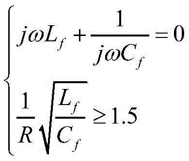
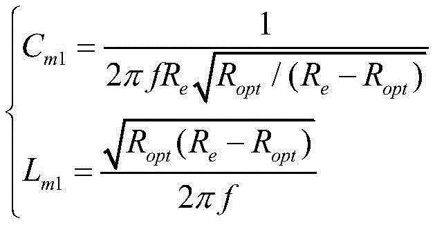
所述初级阻抗匹配模块5,包括第一匹配电感Lf、第一匹配电容Cf、第二匹配电感Lm2和第二匹配电容Cm2;所述第一匹配电感Lf的一端与所述第一开关MOS管S1源极端相连,另一端与所述第一匹配电容Cf的一端相连;所述第二匹配电容Cm2的一端与所述第一匹配电容Cf的另一端以及所述第二匹配电感Lm2的一端相连,该Cm2的另一端接地,所述第二匹配电感Lm2的另一端与所述初级谐振补偿电容Cp的一端相连;如前所述,所述DC_DC降压模块12的应用与其输出输入电压差有关,其转化效率的大小决定了其适用与否,经过市电输入模块后,DC_DC降压模块的输入电压为308V±10%的高压直流电,为了使其适用于无线能量传输系统,需要保证其输入输出电压差在一个较为合理的范围之内,即其输出电压不能太小;然而当SS拓扑磁谐振无线能量传输系统对应较大负载时,由于其自身特性的原因,其所述WPT模块对应的初级反射阻抗很小,即其输入端的等效端口阻抗很小,这意味着在满足一定功率输出下其只需要很小的供电电压。所述初级阻抗匹配模块6的作用就是在于将原所述初级逆变模块2的输出阻抗由原来较小的所述WPT模块3的输入阻抗提升为一个较大的阻抗值,由此提高在满足一定功率的输出情况下所述初级逆变模块2所需的电压,也即提高所述DC_DC降压模块5的输出电压,使其满足此时在SS拓扑磁谐振无线能量传输系统中的应用。参照图2,所述初级阻抗匹配模块6的具体设计原理和过程如下:The primary
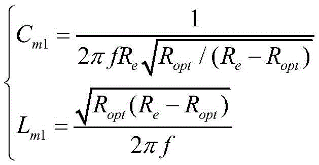
如图2所示,从电容Cm2左侧看进去的所述初级阻抗匹配模块6的输入端口阻抗可表示为As shown in FIG. 2 , the input port impedance of the primary
Ze2=Re2+jXe2 (1)Z e2 =R e2 +jX e2 (1)
令所述WPT模块3输入端的等效端口阻抗为Rep,为了将这种阻抗变换网络应用在对Rep的变换上,则必须使上式的等效阻抗虚部为0,且实部等于我们所需要的较大的目标匹配等效阻抗Re2,即对于上式而言,需满足Let the equivalent port impedance of the input end of the
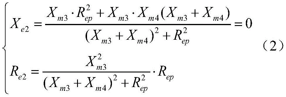
其中,Xm3、Xm4分别为第二匹配电容Cm2和第二匹配电感Lm2的电抗值。Wherein, X m3 and X m4 are the reactance values of the second matching capacitor C m2 and the second matching inductance L m2 , respectively.
对上述方程组而言,只有当Re2>Rep时才有实数解,此时匹配网络的参数为For the above equations, there is a real solution only when R e2 > R ep , and the parameters of the matching network are:
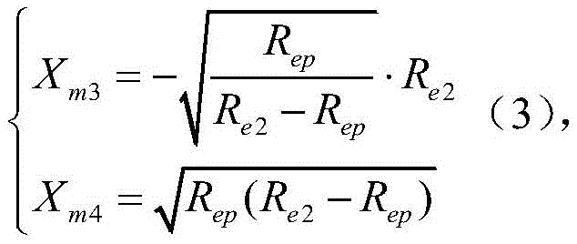
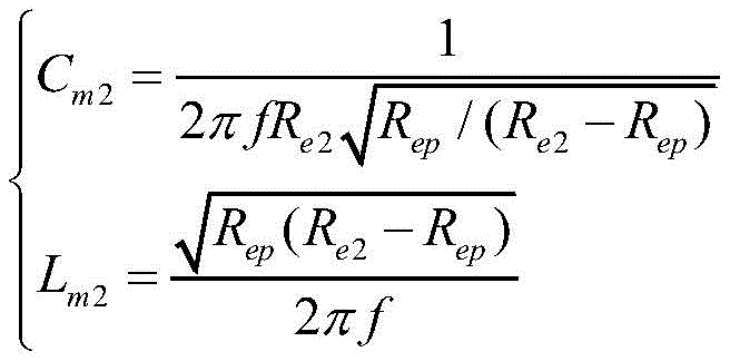
即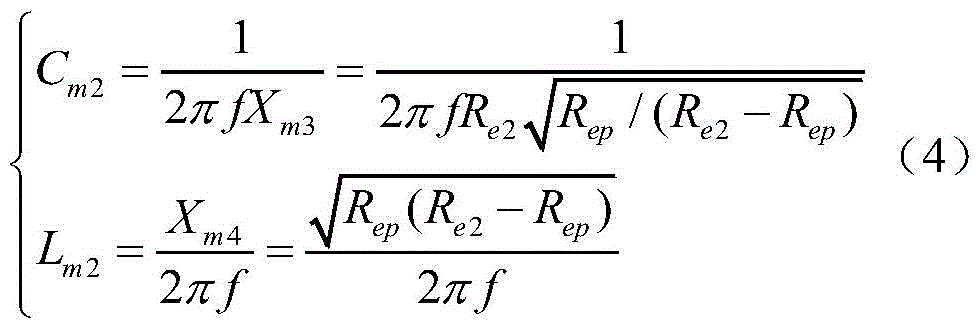
其中,f为所述WPT模块的谐振频率。Wherein, f is the resonant frequency of the WPT module.
但此时完整的所述初级阻抗匹配模块6还需要包含所述初级阻抗匹配模块6中的第一匹配电感Lf、第一匹配电容Cf,因为所述初级逆变模块2输出的为高频方波电压,需要设计由第一匹配电感Lf、第一匹配电容Cf组成的谐振滤波网络,将其输出的高频方波电压滤波变成接近标准的正弦交流电,否则,此阻抗匹配结果将非常不准确。此时LC参数的设计可按照But at this time, the complete primary

进行设计,R为所述初级阻抗匹配模块5输出端的等效端口阻抗,且R=Re2,此处Re2被匹配到一个较大的阻抗值,以此使得所述初级逆变模块2前级供电所需供电电压增大,在所述市电输入模块11的基础上加入较为简单的所述DC_DC降压模块12就可以高效做到,从而使得前级供电模块复杂度减小,且当所述初级逆变模块2所需电压越高,即所述DC_DC降压模块12降压输出的电压值越高,其降压转换效率越高。Design, R is the equivalent port impedance of the output end of the primary
所述WPT模块3,包括相互串联的初级发射线圈Lp和其初级谐振补偿电容Cp,以及相互串联的次级接收线圈Ls和其次级谐振补偿电容Cs,且相互串联的初级发射线圈Lp和其初级谐振补偿电容Cp与相互串联的次级接收线圈Ls和其次级谐振补偿电容Cs相对排布;具体工作时,初级发射线圈Lp和其初级谐振补偿电容Cp构成初级谐振回路,次级接收线圈Ls和其次级谐振补偿电容Cs构成次级谐振回路,初级逆变模块输出交流电压频率与磁耦合谐振部分中两个谐振回路的固有频率相同,初级逆变模块注入的能量在初级端谐振回路中进行电能—磁场能的变换,当初级发射线圈Lp产生的电磁场被具有相同共振频率的次级端谐振回路感应到时,两个谐振回路即发生共振,并在电感线圈间以电磁场的方式进行能量的传输,最终再经接收端谐振回路磁场能-电能的转换为后级模块供电。在WPT模块中,常用线圈结构为平面螺旋线圈和立体螺旋线圈,一旦线圈确定,谐振频率确定,则其传输特性确定。要想获得更好的传输特性,如效率等,则需要对传统线圈形式进行改进。参照图3,其中的初级发射线圈Ls,包括初级U型磁芯和螺旋缠绕在初级U型磁芯底部的导线,次级接收线圈Lp,包括次级U型磁芯和螺旋缠绕在次级U型磁芯底部的导线,且初级U型磁芯和次级U型磁芯的开口相对,线圈导线线材为单股铜线或多股利兹线。具体可选的,本发明中初次级线圈与磁芯保持一致,线圈线径(直径)r为1mm,匝数为28匝,磁芯截面为正方形,边长D1=18mm,长度D2=44mm,D3=20mm,间距d=30mm。WPT模块的效率与初级和次级线圈间的互感等参量有关,在其他参量都确定的情况下,其互感越大,传输效率越高,对比传统线圈形式,螺旋缠绕有导线的初级U型磁芯和次级U型磁芯的开口相对,优化了线圈之间的磁耦合路径,增大了线圈之间的互感,其磁场耦合效应进一步增强,从而提高了WPT模块的传输效率。The
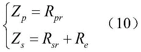
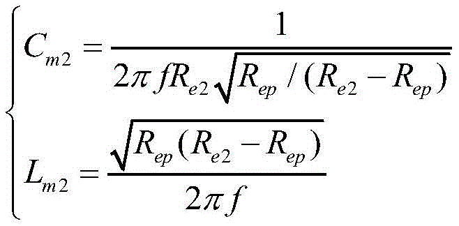
所述次级阻抗匹配模块6,包括第三匹配电感Lm1以及与Lm1一端相连的第三匹配电容Cm1;所述第三匹配电容Cm1另一端与所述次级整流滤波模块4中所述整流桥输入端连接,第三匹配电感Lm1的另一端与所述次级谐振补偿电容的一端相连;所述次级阻抗匹配模块6的作用是将所述WPT模块3的输出端口阻抗匹配到其最佳负载点上,因为其对应不同负载的效率不同,实际应用的供电负载很难刚好位于其最佳负载点上,将其匹配到最佳负载点能够有效的实现所设计的所述WPT模块3的最大效率传输。参照图4,本发明中采用SS拓扑的WPT模块可等效为图4所示的原理电路图,其中Rpr表示初级发射线圈的内阻,Rsr表示次级接收线圈的内阻,Re为级联在后级输出端的等效阻抗,也即上述次级整流桥滤波模块4输入端的等效阻抗,ω是WPT模块的谐振角频率,M为两个线圈之间的互感。The secondary
Zp和Zs分别代表两端阻抗,那么由KVL可得到下面的方程:Z p and Z s represent the impedance at both ends respectively, then the following equation can be obtained from KVL:
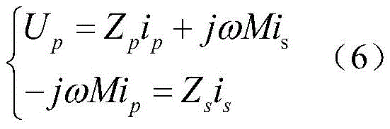
两式联立可推出Two types can be launched simultaneously
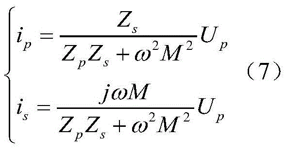
由戴维宁定理,电源的等效负载为By Thevenin's theorem, the equivalent load of the power supply is

其中,第二项为次级折算到发射端的等效反射阻抗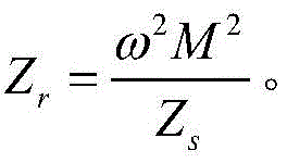
Zp和Zs可分别表示为 Zp and Zs can be expressed as

根据串联谐振条件
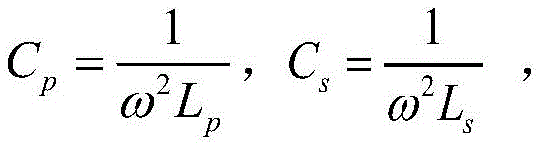
电源等效负载可简化为The power equivalent load can be simplified to

此Zep即为所述WPT模块3输入端的等效端口阻抗Rep,由此式可知,Rep与Re成反比关系,所述WPT模块3的输出端端口阻抗越大,也即对应的用电负载越大,其输入端的等效端口阻抗越小,一定功率输出下其所需的供电电压就越小。This Zep is the equivalent port impedance R ep of the input end of the
定义磁谐振机构的效率η为Re吸收的有功功率Pe和初级侧输入端提供的有功功率Pp之比,则可得The efficiency η of the magnetic resonance mechanism is defined as the ratio of the active power P e absorbed by Re to the active power P p provided by the primary side input, then we can get
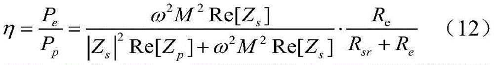
同理谐振条件下可化简为:Under the same resonance condition, it can be simplified as:

发射线圈与接收线圈各自的品质因数分别为


由此,本发明设计所述次级阻抗匹配模块6,用于将所述WPT模块的输出端口阻抗匹配到其最佳负载点上,以此实现WPT模块的最大效率传输。参照图5,从第三匹配电感Lm1左侧看进去的所述次级阻抗匹配模块7的输入端口阻抗可表示为Therefore, the present invention designs the secondary
Ze1=Re1+jXe1 (15)Z e1 =R e1 +jX e1 (15)
为了将这种阻抗变换网络应用在对Re的变换上,则必须使上式的等效阻抗虚部为0,且实部等于我们需要的目标匹配阻抗Ropt,即对于上式而言,需满足In order to apply this impedance transformation network to the transformation of Re , the imaginary part of the equivalent impedance of the above formula must be 0, and the real part is equal to the target matching impedance we need R opt , that is, for the above formula, to be satisfied

对上述方程组而言,只有当Ropt<Re时才有实数解,此时匹配网络的参数为For the above equations, there is a real solution only when R opt < Re , and the parameters of the matching network are:
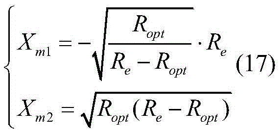
其中,Xm1、Xm2分别为第三匹配电容Cm1和第三匹配电感Lm1的电抗值。Wherein, X m1 and X m2 are the reactance values of the third matching capacitor C m1 and the third matching inductance L m1 , respectively.
即
其中,f为所述WPT模块的谐振频率。Wherein, f is the resonant frequency of the WPT module.
所述次级整流滤波模块4,包括由四个肖特基或快恢复类型的二极管构成的整流桥,以及与整流桥输出端相连的第一滤波电容CL,所述第一滤波电容CL的另一端接地;所述次级整流滤波模块4的输入为高频交流电,一般的二极管用于整流极易损坏且损耗较大,所以这里需要采用损耗较小且恢复时间较快的肖特基或快恢复类型的二极管;所述次级整流滤波模块4将次级接收到的高频交流电转化为平滑稳定的直流电供给用电负载RL,一般地,其输入端等效端口阻抗Re满足关系式
以下结合仿真实验,对本发明的技术效果作进一步说明:Below in conjunction with the simulation experiment, the technical effect of the present invention is further described:
1、仿真条件及内容:1. Simulation conditions and content:
1.1现在PSPICE商业软件中搭建如图1所示的系统电路,令输出功率为30W,负载RL为50欧姆,CL为100uF,初级逆变模块输出端口阻抗即初级阻抗匹配模块的目标匹配等效阻抗Re2为100欧姆,所设计的WPT系统初级线圈Lp为121.52uH、串联谐振补偿电容Cp为83.4nF,谐振频率为50k,内阻Rpr为0.06欧姆,次级线圈Lp=Ls,补偿电容Cp=Cs,内阻Rsr=Rpr,耦合系数k=0.105,Cb为188.8uF,Lb为1.73mH,C为1000uF,另外综合上述式(4)(5)(11)(16)(19)计算可得其他参数为Cm1=237.34nF,Lm1=38.48uF,Cm2=155.08nF,Lm2=62.69uF,Lf=590uF,Cf=17.15nF。1.1 Now build the system circuit shown in Figure 1 in the PSPICE commercial software, let the output power be 30W, the load R L is 50 ohms, C L is 100uF, the output port impedance of the primary inverter module is the target matching of the primary impedance matching module, etc. The effective impedance Re2 is 100 ohms, the primary coil Lp of the designed WPT system is 121.52uH, the series resonance compensation capacitor Cp is 83.4nF, the resonant frequency is 50k, the internal resistance Rpr is 0.06 ohms, and the secondary coil Lp = L s , compensation capacitance C p =C s , internal resistance R sr =R pr , coupling coefficient k=0.105, C b is 188.8uF, L b is 1.73mH, C is 1000uF, and the above equations (4) (5) )(11)(16)(19) The other parameters can be calculated as C m1 =237.34nF, L m1 =38.48uF, C m2 =155.08nF, L m2 =62.69uF, L f =590uF, C f =17.15nF .
1.2仿真加入次级阻抗匹配模块与未加时的WPT模块输入输出端口的平均功率,仿真结果如图6所示。1.2 Simulation The average power of the input and output ports of the secondary impedance matching module and the WPT module without time addition is added. The simulation results are shown in Figure 6.
1.3仿真加入初级阻抗匹配模块与未加时初级逆变模块所需的供电电压值,仿真结果如图7所示。1.3 Simulation Add the power supply voltage value required by the primary impedance matching module and the primary inverter module without adding time. The simulation results are shown in Figure 7.
2、仿真结果:2. Simulation results:
如图6所示,图6(a)为加入次级阻抗匹配模块时WPT模块的输入端口与输出端口的平均功率曲线,则其效率为输出/输入=31.028/32.100=0.9666;图6(b)为未加次级阻抗匹配模块时WPT模块的输入端口与输出端口的平均功率曲线,同理可得其效率为0.8646,可见,次级阻抗匹配模块的引入较大程度上提高了WPT模块的传输效率。As shown in Figure 6, Figure 6(a) is the average power curve between the input port and the output port of the WPT module when the secondary impedance matching module is added, then its efficiency is output/input=31.028/32.100=0.9666; Figure 6(b) ) is the average power curve of the input port and output port of the WPT module without the secondary impedance matching module, and the efficiency can be obtained as 0.8646 in the same way. It can be seen that the introduction of the secondary impedance matching module has greatly improved the WPT module. transmission efficiency.
如图7所示,图7(a)为加入初级阻抗匹配模块时初级逆变模块输入端所需的电压值,为122V,此时电压较高,与308V±10%的电压相比相差不是特别大,能够维持DC_DC模块的输入输出电压差在一个合理的范围,使得市电输入模块加DC_DC降压模块共同构成的输入电源模块得以适用,简化系统;而图7(b)为未加初级阻抗匹配模块时初级逆变模块输入端所需的电压值(最终负载输出功率30W不变),此时仅为27.3V,此时DC_DC降压模块将不再适用于初逆变模块前端的供电。As shown in Figure 7, Figure 7(a) is the voltage value required by the input terminal of the primary inverter module when the primary impedance matching module is added, which is 122V. At this time, the voltage is relatively high, and the difference compared with the voltage of 308V±10% is not Especially large, it can maintain the input and output voltage difference of the DC_DC module within a reasonable range, so that the input power module composed of the mains input module and the DC_DC step-down module can be applied, and the system can be simplified; When the impedance matching module is used, the voltage value required by the input terminal of the primary inverter module (the output power of the final load is 30W unchanged) is only 27.3V at this time. At this time, the DC_DC step-down module will no longer be suitable for the power supply of the front end of the primary inverter module. .
Claims (4)
Priority Applications (1)
| Application Number | Priority Date | Filing Date | Title |
|---|---|---|---|
| CN201910254185.1A CN109921523B (en) | 2019-03-30 | 2019-03-30 | Magnetic resonance wireless energy transfer system based on SS topology |
Applications Claiming Priority (1)
| Application Number | Priority Date | Filing Date | Title |
|---|---|---|---|
| CN201910254185.1A CN109921523B (en) | 2019-03-30 | 2019-03-30 | Magnetic resonance wireless energy transfer system based on SS topology |
Publications (2)
| Publication Number | Publication Date |
|---|---|
| CN109921523A CN109921523A (en) | 2019-06-21 |
| CN109921523B true CN109921523B (en) | 2022-08-12 |
Family
ID=66967905
Family Applications (1)
| Application Number | Title | Priority Date | Filing Date |
|---|---|---|---|
| CN201910254185.1A Active CN109921523B (en) | 2019-03-30 | 2019-03-30 | Magnetic resonance wireless energy transfer system based on SS topology |
Country Status (1)
| Country | Link |
|---|---|
| CN (1) | CN109921523B (en) |
Families Citing this family (1)
| Publication number | Priority date | Publication date | Assignee | Title |
|---|---|---|---|---|
| CN110620416B (en) * | 2019-09-10 | 2024-03-01 | 上海科技大学 | A single-stage isolated wireless fast charging system |
Citations (3)
| Publication number | Priority date | Publication date | Assignee | Title |
|---|---|---|---|---|
| CN1996711A (en) * | 2006-12-08 | 2007-07-11 | 广州电器科学研究院 | Inductive coupled wireless power transfer device |
| CN101699708A (en) * | 2002-05-13 | 2010-04-28 | 捷通国际有限公司 | Contact-less power transfer and method |
| CN204992792U (en) * | 2015-03-01 | 2016-01-20 | 华南理工大学 | Add bi -polar impedance transforming network's resonant mode wireless power transmission system |
Family Cites Families (2)
| Publication number | Priority date | Publication date | Assignee | Title |
|---|---|---|---|---|
| US10266060B2 (en) * | 2016-02-19 | 2019-04-23 | Ford Global Technologies, Llc | SS-L wireless power transfer compensation circuit |
| KR20170110866A (en) * | 2016-03-24 | 2017-10-12 | 현대자동차주식회사 | Primary coil circuit for wireless power transfer and ground assembly and manufacturing method therefor using the same |
-
2019
- 2019-03-30 CN CN201910254185.1A patent/CN109921523B/en active Active
Patent Citations (3)
| Publication number | Priority date | Publication date | Assignee | Title |
|---|---|---|---|---|
| CN101699708A (en) * | 2002-05-13 | 2010-04-28 | 捷通国际有限公司 | Contact-less power transfer and method |
| CN1996711A (en) * | 2006-12-08 | 2007-07-11 | 广州电器科学研究院 | Inductive coupled wireless power transfer device |
| CN204992792U (en) * | 2015-03-01 | 2016-01-20 | 华南理工大学 | Add bi -polar impedance transforming network's resonant mode wireless power transmission system |
Also Published As
| Publication number | Publication date |
|---|---|
| CN109921523A (en) | 2019-06-21 |
Similar Documents
| Publication | Publication Date | Title |
|---|---|---|
| CN104753152B (en) | The induction type charging system of constant current constant voltage Compound Topology | |
| CN109130903B (en) | A low-voltage high-power wireless charging system with double-sided LCCL-T topology | |
| CN109617190B (en) | Anti-offset battery wireless charging system based on constant current-constant voltage composite topology | |
| CN105720582B (en) | A kind of particular harmonic eliminates radio energy transmission system and its design method | |
| WO2018126617A1 (en) | Wireless charging circuit with constant-current constant-voltage compound topology | |
| CN111898289B (en) | A Design Method of LCC-S Topology Parameters for Long-distance Wireless Charging | |
| WO2022116413A1 (en) | Variable circuit topology capable of switching wireless power transmission coil and compensation capacitor | |
| CN109638978B (en) | A high-efficiency constant-voltage and constant-current switching wireless charging topology | |
| CN104868611B (en) | Resonant wireless electric energy transmission system based on double-E type power amplifier | |
| CN111106676A (en) | Magnetic coupling mechanism parameter multi-objective optimization method of LCC-S type MC-WPT system | |
| CN106549509B (en) | Magnetic coupling resonant wireless energy transmission device and method | |
| CN107959355A (en) | The radio energy transmission system that a kind of magnetic field coupling-type is combined with field coupling formula | |
| CN206992959U (en) | bidirectional resonant converter | |
| CN115632492A (en) | Wireless power transmission reconfigurable topological structure and system based on multi-resonance compensation | |
| CN113572274A (en) | Resonant wireless power transmission system with LCC-LCLCC compensation network | |
| CN117118093A (en) | A multi-coil wireless power transmission system and its compensation parameter optimization method | |
| CN110896249A (en) | Asymmetric four-coil resonator and wireless power transfer system with asymmetric four-coil resonator | |
| CN105186705A (en) | High-efficiency electric energy transmitting terminal, non-contact electric energy transmission device, and electric energy transmission method | |
| CN110112836A (en) | A kind of magnet coupled resonant type wireless transmission system and control method | |
| CN109921523B (en) | Magnetic resonance wireless energy transfer system based on SS topology | |
| CN206559146U (en) | Magnet coupled resonant type wireless energy transmission equipment | |
| CN108183616A (en) | A Low Stress High Frequency DC/DC Power Converter Based on Transformer Leakage Inductance | |
| CN204992793U (en) | A device for wireless power transmission | |
| CN116470655A (en) | Efficient anti-offset magnetic resonance type wireless power transmission system and control method thereof | |
| CN210839080U (en) | High-voltage ultra-thin wireless power transmission system |
Legal Events
| Date | Code | Title | Description |
|---|---|---|---|
| PB01 | Publication | ||
| PB01 | Publication | ||
| SE01 | Entry into force of request for substantive examination | ||
| SE01 | Entry into force of request for substantive examination | ||
| GR01 | Patent grant | ||
| GR01 | Patent grant |