CN109842306B - Single-input multi-output direct-current power supply system and related voltage reduction regulation control circuit - Google Patents
Single-input multi-output direct-current power supply system and related voltage reduction regulation control circuit Download PDFInfo
- Publication number
- CN109842306B CN109842306B CN201711430495.1A CN201711430495A CN109842306B CN 109842306 B CN109842306 B CN 109842306B CN 201711430495 A CN201711430495 A CN 201711430495A CN 109842306 B CN109842306 B CN 109842306B
- Authority
- CN
- China
- Prior art keywords
- buck
- signal
- voltage
- buck regulator
- pwm
- Prior art date
- Legal status (The legal status is an assumption and is not a legal conclusion. Google has not performed a legal analysis and makes no representation as to the accuracy of the status listed.)
- Active
Links
- 239000003990 capacitor Substances 0.000 description 22
- 238000010586 diagram Methods 0.000 description 8
- 238000006243 chemical reaction Methods 0.000 description 5
- 102100029469 WD repeat and HMG-box DNA-binding protein 1 Human genes 0.000 description 4
- 101710097421 WD repeat and HMG-box DNA-binding protein 1 Proteins 0.000 description 4
- 230000004913 activation Effects 0.000 description 3
- 230000000694 effects Effects 0.000 description 3
- 238000013459 approach Methods 0.000 description 2
- 238000000034 method Methods 0.000 description 1
- 238000012986 modification Methods 0.000 description 1
- 230000004048 modification Effects 0.000 description 1
- 239000002699 waste material Substances 0.000 description 1
Images


Classifications
-
- H—ELECTRICITY
- H02—GENERATION; CONVERSION OR DISTRIBUTION OF ELECTRIC POWER
- H02M—APPARATUS FOR CONVERSION BETWEEN AC AND AC, BETWEEN AC AND DC, OR BETWEEN DC AND DC, AND FOR USE WITH MAINS OR SIMILAR POWER SUPPLY SYSTEMS; CONVERSION OF DC OR AC INPUT POWER INTO SURGE OUTPUT POWER; CONTROL OR REGULATION THEREOF
- H02M1/00—Details of apparatus for conversion
- H02M1/36—Means for starting or stopping converters
-
- H—ELECTRICITY
- H02—GENERATION; CONVERSION OR DISTRIBUTION OF ELECTRIC POWER
- H02M—APPARATUS FOR CONVERSION BETWEEN AC AND AC, BETWEEN AC AND DC, OR BETWEEN DC AND DC, AND FOR USE WITH MAINS OR SIMILAR POWER SUPPLY SYSTEMS; CONVERSION OF DC OR AC INPUT POWER INTO SURGE OUTPUT POWER; CONTROL OR REGULATION THEREOF
- H02M1/00—Details of apparatus for conversion
- H02M1/14—Arrangements for reducing ripples from DC input or output
-
- H—ELECTRICITY
- H02—GENERATION; CONVERSION OR DISTRIBUTION OF ELECTRIC POWER
- H02M—APPARATUS FOR CONVERSION BETWEEN AC AND AC, BETWEEN AC AND DC, OR BETWEEN DC AND DC, AND FOR USE WITH MAINS OR SIMILAR POWER SUPPLY SYSTEMS; CONVERSION OF DC OR AC INPUT POWER INTO SURGE OUTPUT POWER; CONTROL OR REGULATION THEREOF
- H02M1/00—Details of apparatus for conversion
- H02M1/32—Means for protecting converters other than automatic disconnection
-
- H—ELECTRICITY
- H02—GENERATION; CONVERSION OR DISTRIBUTION OF ELECTRIC POWER
- H02M—APPARATUS FOR CONVERSION BETWEEN AC AND AC, BETWEEN AC AND DC, OR BETWEEN DC AND DC, AND FOR USE WITH MAINS OR SIMILAR POWER SUPPLY SYSTEMS; CONVERSION OF DC OR AC INPUT POWER INTO SURGE OUTPUT POWER; CONTROL OR REGULATION THEREOF
- H02M3/00—Conversion of DC power input into DC power output
- H02M3/02—Conversion of DC power input into DC power output without intermediate conversion into AC
- H02M3/04—Conversion of DC power input into DC power output without intermediate conversion into AC by static converters
- H02M3/10—Conversion of DC power input into DC power output without intermediate conversion into AC by static converters using discharge tubes with control electrode or semiconductor devices with control electrode
- H02M3/145—Conversion of DC power input into DC power output without intermediate conversion into AC by static converters using discharge tubes with control electrode or semiconductor devices with control electrode using devices of a triode or transistor type requiring continuous application of a control signal
- H02M3/155—Conversion of DC power input into DC power output without intermediate conversion into AC by static converters using discharge tubes with control electrode or semiconductor devices with control electrode using devices of a triode or transistor type requiring continuous application of a control signal using semiconductor devices only
- H02M3/156—Conversion of DC power input into DC power output without intermediate conversion into AC by static converters using discharge tubes with control electrode or semiconductor devices with control electrode using devices of a triode or transistor type requiring continuous application of a control signal using semiconductor devices only with automatic control of output voltage or current, e.g. switching regulators
- H02M3/157—Conversion of DC power input into DC power output without intermediate conversion into AC by static converters using discharge tubes with control electrode or semiconductor devices with control electrode using devices of a triode or transistor type requiring continuous application of a control signal using semiconductor devices only with automatic control of output voltage or current, e.g. switching regulators with digital control
-
- H—ELECTRICITY
- H02—GENERATION; CONVERSION OR DISTRIBUTION OF ELECTRIC POWER
- H02M—APPARATUS FOR CONVERSION BETWEEN AC AND AC, BETWEEN AC AND DC, OR BETWEEN DC AND DC, AND FOR USE WITH MAINS OR SIMILAR POWER SUPPLY SYSTEMS; CONVERSION OF DC OR AC INPUT POWER INTO SURGE OUTPUT POWER; CONTROL OR REGULATION THEREOF
- H02M3/00—Conversion of DC power input into DC power output
- H02M3/02—Conversion of DC power input into DC power output without intermediate conversion into AC
- H02M3/04—Conversion of DC power input into DC power output without intermediate conversion into AC by static converters
- H02M3/10—Conversion of DC power input into DC power output without intermediate conversion into AC by static converters using discharge tubes with control electrode or semiconductor devices with control electrode
- H02M3/145—Conversion of DC power input into DC power output without intermediate conversion into AC by static converters using discharge tubes with control electrode or semiconductor devices with control electrode using devices of a triode or transistor type requiring continuous application of a control signal
- H02M3/155—Conversion of DC power input into DC power output without intermediate conversion into AC by static converters using discharge tubes with control electrode or semiconductor devices with control electrode using devices of a triode or transistor type requiring continuous application of a control signal using semiconductor devices only
- H02M3/156—Conversion of DC power input into DC power output without intermediate conversion into AC by static converters using discharge tubes with control electrode or semiconductor devices with control electrode using devices of a triode or transistor type requiring continuous application of a control signal using semiconductor devices only with automatic control of output voltage or current, e.g. switching regulators
- H02M3/158—Conversion of DC power input into DC power output without intermediate conversion into AC by static converters using discharge tubes with control electrode or semiconductor devices with control electrode using devices of a triode or transistor type requiring continuous application of a control signal using semiconductor devices only with automatic control of output voltage or current, e.g. switching regulators including plural semiconductor devices as final control devices for a single load
- H02M3/1584—Conversion of DC power input into DC power output without intermediate conversion into AC by static converters using discharge tubes with control electrode or semiconductor devices with control electrode using devices of a triode or transistor type requiring continuous application of a control signal using semiconductor devices only with automatic control of output voltage or current, e.g. switching regulators including plural semiconductor devices as final control devices for a single load with a plurality of power processing stages connected in parallel
-
- H—ELECTRICITY
- H02—GENERATION; CONVERSION OR DISTRIBUTION OF ELECTRIC POWER
- H02M—APPARATUS FOR CONVERSION BETWEEN AC AND AC, BETWEEN AC AND DC, OR BETWEEN DC AND DC, AND FOR USE WITH MAINS OR SIMILAR POWER SUPPLY SYSTEMS; CONVERSION OF DC OR AC INPUT POWER INTO SURGE OUTPUT POWER; CONTROL OR REGULATION THEREOF
- H02M1/00—Details of apparatus for conversion
- H02M1/0067—Converter structures employing plural converter units, other than for parallel operation of the units on a single load
- H02M1/008—Plural converter units for generating at two or more independent and non-parallel outputs, e.g. systems with plural point of load switching regulators
-
- H—ELECTRICITY
- H02—GENERATION; CONVERSION OR DISTRIBUTION OF ELECTRIC POWER
- H02M—APPARATUS FOR CONVERSION BETWEEN AC AND AC, BETWEEN AC AND DC, OR BETWEEN DC AND DC, AND FOR USE WITH MAINS OR SIMILAR POWER SUPPLY SYSTEMS; CONVERSION OF DC OR AC INPUT POWER INTO SURGE OUTPUT POWER; CONTROL OR REGULATION THEREOF
- H02M1/00—Details of apparatus for conversion
- H02M1/0083—Converters characterised by their input or output configuration
- H02M1/009—Converters characterised by their input or output configuration having two or more independently controlled outputs
Landscapes
- Engineering & Computer Science (AREA)
- Power Engineering (AREA)
- Dc-Dc Converters (AREA)
- Inverter Devices (AREA)
Abstract
一种降压调节控制电路,用于一单输入多输出直流电源供应系统,该单输入多输出电源供应系统的一第一降压调节器于一软启动阶段时,当一第二降压调节器的一第二高端开关维持关闭状态时,该降压调节控制电路可控制该第一降压调节器的一第一高端开关由关闭状态切换为导通状态。如此可避免该第一高端开关及该第二高端开关同时由关闭状态切换为导通状态,以降低浪涌电流。
A buck regulation control circuit for a single-input multiple-output DC power supply system. When a first buck regulator of the single-input multiple-output power supply system is in a soft-start stage, when a second buck regulator When a second high-side switch of the regulator remains in a closed state, the buck regulation control circuit can control a first high-side switch of the first buck regulator to switch from a closed state to a conductive state. This can prevent the first high-side switch and the second high-side switch from switching from the off state to the on state at the same time, thereby reducing the surge current.
Description
技术领域technical field
本发明是指一种单输入多输出的直流电源供应系统及相关降压调节控制电路,尤指一种可降低开机瞬间的浪涌电流,并兼顾纹波电压的单输入多输出的直流电源供应系统及相关降压调节控制电路。The invention refers to a single-input multiple-output DC power supply system and a related step-down regulation control circuit, especially a single-input multiple-output DC power supply that can reduce the inrush current at the moment of startup and take into account the ripple voltage System and related buck regulator control circuit.
背景技术Background technique
单输入多输出的直流电源供应系统在现有电子系统中已广泛应用,举凡笔记本电脑、桌面计算机、服务器系统或是其他计算机系统等,其多以一较高的直流电压作为输入来源,再经由多个脉冲宽度调变(Pulse Width Modulation,PWM)的降压调节器(BuckVoltage Regulator)来转换出不同的输出电压源,以供应系统内部组件所需的电源。例如,电源供应器(Power Supply Unit,PSU)或是电池组(Battery Pack)可将单一交流电源转换成较高电压准位的直流电压源,再利用多个降压调节器降转出多个低电压准位的直流电压源。Single-input multiple-output DC power supply systems have been widely used in existing electronic systems, such as notebook computers, desktop computers, server systems or other computer systems, which mostly use a higher DC voltage as the input source, and then pass A plurality of Pulse Width Modulation (PWM) buck regulators (BuckVoltage Regulator) are used to convert different output voltage sources to supply the power required by the internal components of the system. For example, a power supply unit (PSU) or a battery pack (Battery Pack) can convert a single AC power source into a DC voltage source with a higher voltage level, and then use multiple buck regulators to step down multiple Low voltage level DC voltage source.
图1为习知技术之一降压调节器1的功能方块图。降压调节器1包含一脉冲宽度调变控制器10、一栅极驱动电路11、一高端开关HSW(例如,金氧半场效晶体管(High SideMosFET)、一低端开关LSW、一输出电感L以及一输出电容C。脉冲宽度调变控制器10用来根据一电压启动信号V_EN,产生一脉冲宽度调变信号PWM至栅极驱动电路11。栅极驱动电路11、高端开关HSW、低端开关LSW、输出电感L及输出电容C的组合用来根据脉冲宽度调变信号PWM,将一输入直流电压V_IN转换为一输出直流电压V_OUT。关于电压转换的详细操作应为本领域所熟知,于此不赘述。FIG. 1 is a functional block diagram of a
当降压调节器1处于关闭状态时,输出电容C的初始电压为零伏特。当降压调节器1处于启动状态,且脉冲宽度调变信号PWM为高准位(High level)时,可导通高端开关HSW,使输入直流电压V_IN对应的直流电流I经由高端开关HSW及输出电感L,对输出电容C充电。当高端开关HSW导通时,输出电容C的储存电位(即输出直流电压V_OUT)逐渐由零伏特向上增加,其中输出电容C的瞬间充电电流I可表示为C*(dV_OUT)/(dT),T为充电时间。因为降压调节器1刚启动的瞬间,输出直流电压V_OUT的初始状态为零伏特,因此在此刻的单位时间充电电压dV_OUT/dT将为最大值(dV_OUT趋近于输入直流电压V_IN,且单位充电时间dT趋近于零),所以此时的输出电容C上的瞬间充电电流I也是最大值。随着输出直流电压V_OUT慢慢增加,充电电流I会逐渐降低。When the
浪涌电流(inrush current)指当一个较高准位的输入直流电压开始对电源供应系统内部的等效电容充电时,其瞬间产生的最大电流值。当设计者为了让电源供应系统的各个电压源的纹波电压(ripple voltage)被压抑在可接受的范围内时,往往会尝试增加各个电压源的输出电容值(例如,降压调节器1的输出电容C),以降低其纹波电压。然而,上述设计会导致电源供应系统的等效电容值上升,其中电源供应系统的等效电容值相当于各个降压调节器的输出电容值的总和。电源供应系统的等效电容值越大,所造成的浪涌电流就越大,尤其是当电源供应系统内部所有的降压调节器都在同一时间开启时,可能会导致电源供应器或输入电池组的瞬间输出电流超过该电源供应系统可提供的最大额定电流。假设电源供应系统包含N个降压调节器,当N个高端开关HSW同时导通时,则电源供应系统的浪涌电流可表示为个别输出电容C1、C2、…、Cn的瞬间充电电流的总和I_inrush=I1+…+In=C1*(dV_OUT1)/(dT)+…+Cn*(dV_OUTn)/(dT)。在此情况下,浪涌电流I_inrush可能触发电源供应系统的过电流保护机制(over current protection,OCP),进而导致电源供应系统被强制关闭。Inrush current (inrush current) refers to the maximum current value instantaneously generated when a higher-level input DC voltage begins to charge the equivalent capacitance inside the power supply system. When the designer wants to suppress the ripple voltage of each voltage source of the power supply system within an acceptable range, he often tries to increase the output capacitance value of each voltage source (for example, the
为了解决上述问题,设计者会尝试提高电源供应系统所能输出的最大额定电流与过电流保护点,但这会导致电源供应系统的成本上升,例如须选用规格与成本较高的电子料件以适用较高的最大额定电流。在实际应用中,浪涌电流通常只发生在降压调节器被启动的初始阶段,在输出电压稳定而达到稳定阶段之后,发生较大浪涌电流的机率相对减小许多。然而,上述设计的缺点是为了因应开机瞬间可能发生的高浪涌电流情况,电源供应系统却因此面临过度设计(over design)与成本浪费的问题。此外,当最大额定电流与过电流保护点太高时,将使其失去应有的保护效果,例如过电流越大则输出负载被过电流烧毁失效的风险越大。In order to solve the above problems, designers will try to increase the maximum rated current and overcurrent protection points that the power supply system can output, but this will lead to an increase in the cost of the power supply system. Higher maximum current ratings apply. In practical applications, the inrush current usually only occurs in the initial stage when the buck regulator is started. After the output voltage stabilizes and reaches the stable stage, the probability of a large inrush current is relatively reduced. However, the disadvantage of the above-mentioned design is that in order to cope with the high inrush current situation that may occur at the moment of power-on, the power supply system faces the problems of over-design and waste of cost. In addition, when the maximum rated current and the overcurrent protection point are too high, it will lose its due protection effect. For example, the greater the overcurrent, the greater the risk of the output load being burned out by the overcurrent.
此外,另一个解决方式是尝试减少各个降压调节器的输出电容值,以减少电源供应系统的等效电容值,但这会导致降压调节器的输出电压的纹波电压上升,进而影响输出负载的运作。例如,当纹波电压太高时,无法确保输出负载(例如,计算机系统)在运作过程中,不会因为过高的电压变化而造成运作不正常。因此,减少各个降压调节器的输出电容值的做法,难以确保电源供应系统具有足够的设计限度(design margin)。In addition, another solution is to try to reduce the output capacitance value of each buck regulator to reduce the equivalent capacitance value of the power supply system, but this will cause the ripple voltage of the output voltage of the buck regulator to rise, thereby affecting the output operation of the load. For example, when the ripple voltage is too high, it cannot be ensured that the output load (eg, a computer system) will not operate abnormally due to excessive voltage changes during operation. Therefore, it is difficult to ensure a sufficient design margin for the power supply system by reducing the output capacitance value of each buck regulator.
因此,实有必要提供一种单输入多输出的直流电源供应系统,可降低开机瞬间的浪涌电流,并兼顾降压调节器的纹波电压。Therefore, it is necessary to provide a DC power supply system with a single input and multiple outputs, which can reduce the inrush current at the moment of power-on and take into account the ripple voltage of the buck regulator.
发明内容SUMMARY OF THE INVENTION
因此,本发明的主要目的即在于提供一种单输入多输出的直流电源供应系统及相关控制电路,以降低开机瞬间的浪涌电流。Therefore, the main purpose of the present invention is to provide a single-input multiple-output DC power supply system and a related control circuit, so as to reduce the inrush current at the moment of power-on.
本发明揭露一种第一降压调节控制电路,用于一单输入多输出电源供应系统,包含一开关以及一逻辑电路。该开关耦接于该单输入多输出电源供应系统的一第一降压调节器,用来根据一第一调变启动信号,连接或断开该第一降压调节器的一第一脉冲宽度调变控制器及一栅极驱动电路。该逻辑电路耦接于该开关以及该第一降压调节器,用来根据一第一电压启动信号、该第一脉冲宽度调变控制器产生的一第一脉冲宽度调变信号、该第一脉冲宽度调变控制器产生的一第一电源良好信号以及该单输入多输出电源供应系统的一第二降压调节器产生的一第二脉冲宽度调变信号,产生该第一调变启动信号至该开关;其中该第一降压调节器于一软启动阶段时,当该第二脉冲宽度调变信号为低准位时,该第一调变启动信号控制该第一降压调节器的一第一高端开关由关闭状态切换为导通状态,且该第二降压调节器的一第二高端开关维持关闭状态。The invention discloses a first step-down regulation control circuit for a single-input multiple-output power supply system, comprising a switch and a logic circuit. The switch is coupled to a first buck regulator of the single-input multiple-output power supply system, and is used for connecting or disconnecting a first pulse width of the first buck regulator according to a first modulation activation signal A modulation controller and a gate drive circuit. The logic circuit is coupled to the switch and the first step-down regulator, and is used for starting a signal according to a first voltage, a first PWM signal generated by the first PWM controller, and the first PWM signal. A first power good signal generated by a pulse width modulation controller and a second pulse width modulation signal generated by a second buck regulator of the single-input multiple-output power supply system to generate the first modulation enable signal to the switch; wherein when the first step-down regulator is in a soft-start stage, when the second pulse width modulation signal is at a low level, the first modulation start signal controls the first step-down regulator A first high side switch is switched from an off state to an on state, and a second high side switch of the second buck regulator remains off.
本发明另揭露一种单输入多输出电源供应系统,用来将一直流输入电压转换为复数个直流输出电压,包含一降压调节模块以及一降压调节控制模块。该降压调节模块包含一第一降压调节器以及一第二降压调节器,其中该第一降压调节器用来根据一第一电压启动信号,产生一第一脉冲宽度调变信号,以及根据该第一脉冲宽度调变信号以及一第一调变启动信号,将该直流输入电压转换为一第一直流输出电压。该降压调节控制模块耦接于该降压调节模块,包含一第一降压调节控制电路,耦接于该第一降压调节器以及该第二降压调节器,用来根据该第一电压启动信号、该第一脉冲宽度调变信号、该第一降压调节器产生的一第一电源良好信号以及该第二降压调节器产生的一第二脉冲宽度调变信号,产生该第一调变启动信号至该第一降压调节器;其中该第一降压调节器于一软启动阶段时,当该第二脉冲宽度调变信号为低准位时,则该第一调变启动信号控制该第一降压调节器的一第一高端开关由关闭状态切换为导通状态,且该第二降压调节器的一第二高端开关维持关闭状态。The present invention further discloses a single-input multiple-output power supply system for converting a DC input voltage into a plurality of DC output voltages, comprising a step-down regulation module and a step-down regulation control module. The buck regulator module includes a first buck regulator and a second buck regulator, wherein the first buck regulator is used for generating a first pulse width modulation signal according to a first voltage activation signal, and The DC input voltage is converted into a first DC output voltage according to the first pulse width modulation signal and a first modulation start signal. The buck regulator control module is coupled to the buck regulator module, and includes a first buck regulator control circuit, coupled to the first buck regulator and the second buck regulator, and configured to operate according to the first buck regulator. The voltage enable signal, the first PWM signal, a first power good signal generated by the first buck regulator, and a second PWM signal generated by the second buck regulator generate the first a modulation start signal to the first buck regulator; wherein when the first buck regulator is in a soft start stage, when the second pulse width modulation signal is at a low level, the first modulation The activation signal controls a first high-side switch of the first buck regulator to switch from an off state to an on state, and a second high-side switch of the second buck regulator maintains an off state.
本发明在电源供应系统于软启动阶段时,透过控制各个降压调节器的脉冲宽度调变信号的电压输出时序,避免电源供应系统中所有的高端开关在同一时间导通,以避免过高的浪涌电流问题。对于电源供应系统而言,由于浪涌电流被有效抑制了,因此设计者不需提高电源供应系统所能输出的最大额定电流与过电流保护点。同样的,设计者也不需为了降低浪涌电流而降低每个降压调节器的输出电容值,以确保输出电压的纹波电压可被压抑在足够低的峰对峰值电压范围,进而确保输出负载(例如,计算机系统)可稳定运作。The present invention prevents all high-side switches in the power supply system from being turned on at the same time by controlling the voltage output sequence of the pulse width modulation signal of each step-down regulator when the power supply system is in the soft-start stage, thereby avoiding excessively high the inrush current problem. For the power supply system, since the inrush current is effectively suppressed, the designer does not need to increase the maximum rated current and the overcurrent protection point that the power supply system can output. Similarly, the designer does not need to reduce the output capacitor value of each buck regulator to reduce the inrush current to ensure that the output voltage ripple voltage can be suppressed to a low enough peak-to-peak voltage range to ensure that the output The load (eg, a computer system) can operate stably.
附图说明Description of drawings
图1为习知技术之一降压调节器的功能方块图。FIG. 1 is a functional block diagram of a conventional buck regulator.
图2为本发明实施例一电源供应系统的功能方块图。FIG. 2 is a functional block diagram of a power supply system according to an embodiment of the present invention.
图3为本发明实施例一降压调节模块的栅极驱动电路及一降压调节控制模块的电路图。FIG. 3 is a circuit diagram of a gate driving circuit of a step-down regulation module and a step-down regulation control module according to an embodiment of the present invention.
图4为本发明实施例一降压调节控制电路及一栅极驱动器的电路图。FIG. 4 is a circuit diagram of a step-down regulation control circuit and a gate driver according to an embodiment of the present invention.
具体实施方式Detailed ways
本发明的目的是在电源供应系统于软启动阶段时,避免各个降压调节器的高端开关(例如,金氧半场效晶体管(High Side MosFET)同时导通,如此可避免各个降压调节器的输出等效电容发生加总效应,进而防止过高的浪涌电流发生。详细来说,本发明透过控制各个降压调节器的脉冲宽度调变(Pulse Width Modulation,PWM)信号的电压输出时序,避免电源供应系统中所有的高端开关在同一时间导通,以避免过高的浪涌电流问题。对于电源供应系统而言,由于浪涌电流被有效抑制了,因此设计者不需提高电源供应系统所能输出的最大额定电流与过电流保护点。同样的,设计者也不需为了降低浪涌电流而降低每个降压调节器的输出电容值,以确保输出电压的纹波电压可被压抑在足够低的峰对峰值电压(peak-to-peak voltage)范围,进而确保输出负载(例如,计算机系统)可稳定运作。The purpose of the present invention is to prevent the high-side switches (eg, High Side MosFETs) of each buck regulator from being turned on at the same time when the power supply system is in the soft-start phase, so that each buck regulator can be prevented from being turned on at the same time. The output equivalent capacitance of the PWM produces a summation effect, thereby preventing the occurrence of excessive inrush current. In detail, the present invention controls the voltage output of the Pulse Width Modulation (PWM) signal of each step-down regulator. sequence, to prevent all high-side switches in the power supply system from being turned on at the same time, to avoid the problem of excessive inrush current. For the power supply system, since the inrush current is effectively suppressed, the designer does not need to increase the power supply The maximum rated current and the overcurrent protection point that the supply system can output. Similarly, the designer does not need to reduce the output capacitor value of each buck regulator to reduce the inrush current to ensure that the ripple voltage of the output voltage can be Suppressed to a low enough peak-to-peak voltage range to ensure stable operation of the output load (eg, a computer system).
图2为本发明实施例一电源供应系统2的功能方块图。电源供应系统2包含一降压调节模块20、一交流转直流电压转换器21、一电源控制电路22以及一降压调节控制模块23。FIG. 2 is a functional block diagram of a
交流转直流电压转换器21耦接于降压调节模块20、电源控制电路22以及降压调节控制模块23,用来将一交流电压AC_IN转换为一直流输入电压V_IN至降压调节模块20。此外,交流转直流电压转换器21可分别供应驱动电压给降压调节模块20、电源控制电路22以及降压调节控制模块23。The AC-to-
电源控制电路22耦接于降压调节模块20、交流转直流电压转换器21及降压调节控制模块23,用来产生电压启动信号V_EN1~V_ENn至降压调节模块20及降压调节控制模块23,以及从降压调节模块20接收电源良好信号PWGD1~PWGDn。The
降压调节模块20包含降压调节器BVR1~BVRn,其中降压调节器BVR1~BVRn的电路架构与图1的降压调节器1相同。降压调节模块20耦接于交流转直流电压转换器21、电源控制电路22及降压调节控制模块23,用来根据电压启动信号V_EN1~V_ENn及调变启动信号PWM_EN1~PWM_ENn,将直流输入电压V_IN分别转换为直流输出电压V_OUT1~V_OUTn。当降压调节模块20依序转换出直流输出电压V_OUT1~V_OUTn后,可分别产生电源良好信号PWGD1~PWGDn至电源控制电路22以及降压调节控制模块23,以通报电压转换完成。The
降压调节控制模块23耦接于降压调节模块20、交流转直流电压转换器21及电源控制电路22,用来根据电压启动信号V_EN1~V_ENn、脉冲宽度调变信号PWM1~PWMn、电源良好信号PWGD1~PWGDn,产生调变启动信号PWM_EN1~PWM_ENn至降压调节模块20,以控制降压调节器BVR1~BVRn依序启动,以转换直流输出电压V_OUT1~V_OUTn。The step-down
调变启动信号PWM_EN1~PWM_ENn用来分别控制降压调节器BVR1~BVRn的启动时序,例如软启动时间(Soft Start Time),以避免让所有的降压调节器BVR1~BVRn的所有的高端开关HSW1~HSWn同时导通,进而防止所有的降压调节器BVR1~BVRn的输出电容C1~Cn(未示出)加总效应所造成的浪涌电流。The modulation start-up signals PWM_EN1-PWM_ENn are used to control the start-up sequences of the buck regulators BVR1-BVRn respectively, such as the Soft Start Time, so as to avoid causing all the high-side switches HSW1 of all the buck regulators BVR1-BVRn ~HSWn are turned on at the same time, thereby preventing inrush current caused by the summing effect of the output capacitors C1~Cn (not shown) of all the buck regulators BVR1~BVRn.
具体而言,在个别的降压调节器BVR1~BVRn的软启动时间内,当所有的降压调节器BVR1~BVRn的输出电容C1~Cn的初始电压为零伏特时(即,直流输出电压V_OUT1~V_OUTn皆为零伏特),调变启动信号PWM_EN1~PWM_ENn可控制只有一个降压调节器BVRx的脉冲宽度调变信号PWMx为高准位,仅导通它的高端开关HSWx来对输出电容Cx充电。直到脉冲宽度调变信号PWMx号由高准位转态到低准位(Low Level)之后,另一个降压调节器BVRy才能将其脉冲宽度调变信号PWMy由低准位转态成高准位,导通它的高端开关HSWy来对输出电容Cy充电。Specifically, during the soft-start time of the individual buck regulators BVR1 ˜BVRn, when the initial voltages of the output capacitors C1 ˜Cn of all the buck regulators BVR1 ˜BVRn are zero volts (ie, the DC output voltage V_OUT1 ~V_OUTn are all zero volts), the modulation enable signals PWM_EN1~PWM_ENn can control the pulse width modulation signal PWMx of only one buck regulator BVRx to be high, and only turn on its high-side switch HSWx to charge the output capacitor Cx . Until the pulse width modulation signal PWMx changes from high level to low level, another buck regulator BVRy can change its pulse width modulation signal PWMy from low level to high level , turn on its high-side switch HSWy to charge the output capacitor Cy.
换言之,由于调变启动信号PWM_EN1~PWM_ENn可控制只有一个降压调节器BVRx的脉冲宽度调变信号PWMx为高准位,使降压调节器BVR1~BVRn的高端开关HSW1~HSWn中的一者(即高端开关HSWx)由关闭状态切换为导通状态且其他高端开关HSW1~HSW(x-1)、HSW(x+1)~HSWn维持关闭状态。因此,电源供应系统2的等效电容值仅是降压调节器BVRx启动时的输出电容值Cx,如此可有效降低电源供应系统2的等效电容值,也可避免减少输出电容值Cx,以确保输出电压V_OUTx的纹波电压可被抑制在可接受的范围内,进而确保电源供应系统2的输出负载的运作。In other words, since the modulation enable signals PWM_EN1-PWM_ENn can control the pulse width modulation signal PWMx of only one buck regulator BVRx to be at a high level, one of the high-side switches HSW1-HSWn of the buck regulators BVR1-BVRn ( That is, the high-side switch HSWx) is switched from an off state to an on-state, and the other high-side switches HSW1 ˜HSW(x−1) and HSW(x+1)˜HSWn remain off. Therefore, the equivalent capacitance value of the
值得注意的是,降压调节模块20可根据电压启动信号V_EN1~V_ENn,产生脉冲宽度调变信号PWM1~PWMn,以作为降压调节控制模块23产生调变启动信号PWM_EN1~PWM_ENn的参考依据。详细来说,降压调节控制模块23可根据脉冲宽度调变信号PWM1~PWMn,得知降压调节器BVR1~BVRn是否开始导通其高端开关HSW1~HSWn。例如于软启动时,当脉冲宽度调变信号PWMx为高准位时,降压调节器BVRx开始导通其高端开关HSWx;另一方面,当脉冲宽度调变信号PWMx为低准位时,降压调节器BVRx没有导通其高端开关HSWx。此外,于正式启动时,降压调节器BVRx可正常进行电压转换。It is worth noting that the step-
如此一来,降压调节控制模块23可利用调变启动信号PWM_EN1~PWM_ENn来控制降压调节器BVR1~BVRn的高端开关HSW1~HSWn的导通时序,以避免降压调节器BVR1~BVRn的高端开关HSW1~HSWn同时开启时所造成的浪涌电流,也可确保纹波电压可被抑制在可接受的范围内,进而确保电源供应系统2的输出负载的运作。In this way, the buck
图3为本发明实施例一降压调节模块30及一降压调节控制模块33的电路图。于本实施例中,假设降压调节模块30包含降压调节器BVR1、BVR2(即,n=2),降压调节控制模块33包含降压调节控制电路CTRL1、CTRL2,分别耦接于降压调节器BVR1、BVR2的栅极驱动器DRV1、DRV2,用来控制降压调节器BVR1、BVR2的高端开关HSW1、HSW2的导通时序。于一实施例中,降压调节控制模块33可整合于降压调节模块30;或者,降压调节控制电路CTRL1及CTRL2可分别整合于降压调节器BVR1及BVR2。FIG. 3 is a circuit diagram of a step-down
降压调节器BVR1及BVR2的电路架构相同,于此以降压调节器BVR1为例说明。降压调节器BVR1包含一脉冲宽度调变控制器PGEM1、一栅极驱动电路DRV1、一高端开关HSW1、一低端开关LSW1、一输出电感L1以及一输出电容C1。脉冲宽度调变控制器PGEM1耦接于降压调节控制电路CTRL1,用来根据电压启动信号V_EN1,产生脉冲宽度调变信号PWM1。栅极驱动电路DRV1耦接于降压调节控制电路CTRL1、高端开关HSW1、低端开关LSW1以及输出电感L1,用来根据脉冲宽度调变信号PWM1,导通高端开关HSW1或低端开关LSW1,以产生充电电流来对输出电容C1充电,进而将输入电压V_IN转换为输出电压V_OUT1。The circuit structures of the step-down regulators BVR1 and BVR2 are the same, and the step-down regulator BVR1 is used as an example for description herein. The buck regulator BVR1 includes a pulse width modulation controller PGEM1, a gate driving circuit DRV1, a high-side switch HSW1, a low-side switch LSW1, an output inductor L1 and an output capacitor C1. The pulse width modulation controller PGEM1 is coupled to the step-down regulation control circuit CTRL1 for generating the pulse width modulation signal PWM1 according to the voltage enable signal V_EN1. The gate driving circuit DRV1 is coupled to the step-down regulation control circuit CTRL1, the high-side switch HSW1, the low-side switch LSW1 and the output inductor L1, and is used for turning on the high-side switch HSW1 or the low-side switch LSW1 according to the pulse width modulation signal PWM1, so as to A charging current is generated to charge the output capacitor C1, thereby converting the input voltage V_IN to the output voltage V_OUT1.
降压调节控制电路CTRL1及CTRL2的电路架构相同,于此以降压调节控制电路CTRL1为例说明。降压调节控制电路CTRL1包含一反向器311、一与门(AND gate)312、一或门(OR gate)313以及一开关SW1。反向器311耦接于脉冲宽度调变控制器PGEM2和与门312之间,用来反相脉冲宽度调变信号PWM2的电压准位,以产生反相脉冲宽度调变信号PWM2’。与门312耦接于脉冲宽度调变控制器PGEM1、反向器311及或门313,用来根据电压启动信号V_EN1及反相脉冲宽度调变信号PWM2’,产生一逻辑信号AND1至或门313。或门313耦接于脉冲宽度调变控制器PGEM1、与门312及开关SW1,用来根据电源良好信号PWGD1及逻辑信号AND1,产生调变启动信号PWM_EN1至开关SW1。开关SW1耦接于脉冲宽度调变控制器PGEM1、栅极驱动电路DRV1与或313之间,用来根据调变启动信号PWM_EN1,连接或断开脉冲宽度调变控制器PGEM1及栅极驱动电路DRV1。The circuit structures of the step-down regulation control circuits CTRL1 and CTRL2 are the same, and the step-down regulation control circuit CTRL1 is taken as an example for description herein. The step-down regulation control circuit CTRL1 includes an
关于降压调节器BVR1及降压调节控制电路CTRL1的操作方式简述如下,于软启动阶段,只有当电压启动信号V_EN1及反相脉冲宽度调变信号PWM2’都是高准位的情况下(相当于脉冲宽度调变信号PWM2是低准位),与门312输出的逻辑信号AND1为高准位,可使或门313输出的调变启动信号PWM_EN1为高准位,进而使开关SW1连接脉冲宽度调变控制器PGEM1及栅极驱动电路DRV1。因此,栅极驱动电路DRV1可根据脉冲宽度调变信号PWM1来导通高端开关HSW1或低端开关LSW1,以产生充电电流I1来对输出电容C1充电,进而将输入电压V_IN转换为输出电压V_OUT1。接着,当输出电压V_OUT1已爬升到稳定阶段的输出准位区间时,脉冲宽度调变控制器PGEM1输出电源良好信号PWGD1,以通知电压转换完成。The operation mode of the buck regulator BVR1 and the buck regulator control circuit CTRL1 is briefly described as follows. In the soft start stage, only when the voltage start signal V_EN1 and the inverting pulse width modulation signal PWM2' are at high level ( Equivalent to the pulse width modulation signal PWM2 being low level), the logic signal AND1 output by the AND
换言之,当调变启动信号PWM_EN1为高准位且电源良好信号PWGD1为低准位时,表示此时降压调节器BVR1处于软启动阶段。于软启动阶段时,降压调节器BVR1对应的降压调节控制电路CTRL1可参考另一降压调节器BVR2的脉冲宽度调变信号PWM2,判断是否导通其高端开关HSW1。例如,只有在脉冲宽度调变信号PWM2为低准位(或反相脉冲宽度调变信号PWM2’为高准位)的情况下,开关SW1才会连接脉冲宽度调变控制器PGEM1及栅极驱动电路DRV1,以导通高端开关HSW1。如此一来,降压调节控制电路CTRL1可于软启动阶段,避免高端开关HSW1及HSW2同时导通,以避免浪涌电流。In other words, when the modulation enable signal PWM_EN1 is at a high level and the power good signal PWGD1 is at a low level, it means that the buck regulator BVR1 is in a soft-start stage at this time. During the soft start stage, the buck regulator control circuit CTRL1 corresponding to the buck regulator BVR1 can refer to the pulse width modulation signal PWM2 of another buck regulator BVR2 to determine whether to turn on its high-side switch HSW1. For example, only when the pulse width modulation signal PWM2 is at a low level (or the inverse pulse width modulation signal PWM2' is at a high level), the switch SW1 will be connected to the pulse width modulation controller PGEM1 and the gate driver circuit DRV1 to turn on the high-side switch HSW1. In this way, the step-down regulation control circuit CTRL1 can prevent the high-side switches HSW1 and HSW2 from being turned on at the same time in the soft-start stage, so as to avoid inrush current.
同理,关于降压调节器BVR2及降压调节控制电路CTRL2的操作方式如下,于软启动阶段,只有当电压启动信号V_EN2及反相脉冲宽度调变信号PWM1’都是高准位的情况下(相当于脉冲宽度调变信号PWM1是低准位),与门322输出的逻辑信号AND2为高准位,可使或门323输出的调变启动信号PWM_EN2为高准位,进而使开关SW2连接脉冲宽度调变控制器PGEM2及栅极驱动电路DRV2。因此,栅极驱动电路DRV2可根据脉冲宽度调变信号PWM2来导通高端开关HSW2或低端开关LSW2,以产生充电电流I2来对输出电容C2充电,进而将输入电压V_IN转换为输出电压V_OUT2。接着,当输出电压V_OUT2已爬升到稳定阶段的输出准位区间时,脉冲宽度调变控制器PGEM2输出电源良好信号PWGD2,以通知电压转换完成。In the same way, the operation of the buck regulator BVR2 and the buck regulator control circuit CTRL2 is as follows. In the soft start stage, only when the voltage start signal V_EN2 and the inverting pulse width modulation signal PWM1' are both high level (equivalent to the pulse width modulation signal PWM1 being at a low level), the logic signal AND2 output by the AND
换言之,当调变启动信号PWM_EN2为高准位且电源良好信号PWGD2为低准位时,表示此时降压调节器BVR2处于软启动阶段。于软启动阶段时,降压调节器BVR2对应的降压调节控制电路CTRL2可参考另一降压调节器BVR1的脉冲宽度调变信号PWM1,判断是否导通其高端开关HSW2。例如,只有在脉冲宽度调变信号PWM1为低准位(或反相脉冲宽度调变信号PWM1’为高准位)的情况下,开关SW2才会连接脉冲宽度调变控制器PGEM2及栅极驱动电路DRV2,以导通高端开关HSW2。如此一来,降压调节控制电路CTRL2可于软启动阶段,避免高端开关HSW1及HSW2同时导通,以避免浪涌电流。In other words, when the modulation enable signal PWM_EN2 is at a high level and the power good signal PWGD2 is at a low level, it means that the buck regulator BVR2 is in a soft-start stage at this time. During the soft-start stage, the buck regulator control circuit CTRL2 corresponding to the buck regulator BVR2 can refer to the pulse width modulation signal PWM1 of another buck regulator BVR1 to determine whether to turn on its high-side switch HSW2. For example, only when the pulse width modulation signal PWM1 is at a low level (or the inverse pulse width modulation signal PWM1' is at a high level), the switch SW2 will be connected to the pulse width modulation controller PGEM2 and the gate driver circuit DRV2 to turn on the high-side switch HSW2. In this way, the step-down regulation control circuit CTRL2 can prevent the high-side switches HSW1 and HSW2 from being turned on at the same time in the soft-start stage, so as to avoid inrush current.
因此,透过降压调节控制电路CTRL1及CTRL2的操作,可于软启动阶段时,避免两组降压调节器BVR1及BVR2同时导通其高端开关HSW1及HSW2所造成的浪涌电流,也可确保纹波电压可被抑制在可接受的范围内(例如不须降低输出电容值C1及C2来防止浪涌电流),进而确保电源供应系统的输出负载的运作。Therefore, through the operation of the buck regulator control circuits CTRL1 and CTRL2, in the soft-start stage, the inrush current caused by the two sets of buck regulators BVR1 and BVR2 turning on their high-side switches HSW1 and HSW2 at the same time can be avoided. Ensure that the ripple voltage can be suppressed within an acceptable range (for example, it is not necessary to reduce the output capacitors C1 and C2 to prevent inrush current), thereby ensuring the operation of the output load of the power supply system.
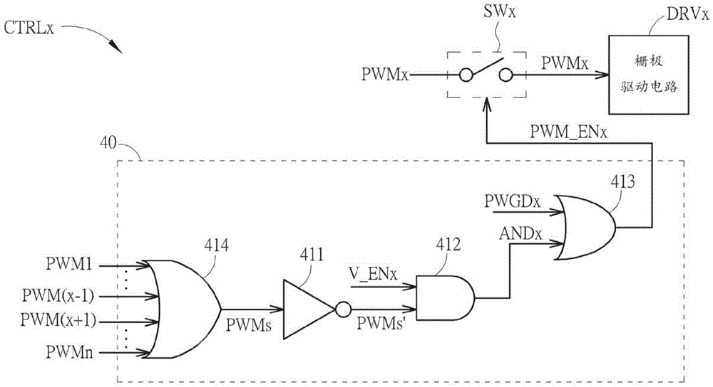
图4为本发明实施例一降压调节控制电路CTRLx及一栅极驱动电路DRVx的电路图。于本实施例中,假设电源供应系统包含n个降压调节器BVR1~BVRn,其中降压调节控制电路CTRLx对应一降压调节器BVRx(图4中未示出),且降压调节器BVRx为n个降压调节器中的一者。FIG. 4 is a circuit diagram of a step-down regulation control circuit CTRLx and a gate driving circuit DRVx according to an embodiment of the present invention. In this embodiment, it is assumed that the power supply system includes n buck regulators BVR1 ˜BVRn, wherein the buck regulator control circuit CTRLx corresponds to a buck regulator BVRx (not shown in FIG. 4 ), and the buck regulator BVRx is one of n buck regulators.
降压调节控制电路CTRLx包含一逻辑电路40以及一开关SWx。逻辑电路40可判断降压调节器BVRx处于软启动阶段,并于软启动阶段时,参考其他降压调节器的脉冲宽度调变信号,产生一调变启动信号PWM_ENx至开关SWx,以输出一脉冲宽度调变信号PWMx。栅极驱动电路DRVx耦接于开关SWx,用来根据脉冲宽度调变信号PWMx,导通自身高端开关或是让自身高端开关维持关闭状态。例如,只有在其他降压调节器的脉冲宽度调变信号为低准位的情况下,逻辑电路40才会控制开关SWx输出脉冲宽度调变信号PWMx来导通自身高端开关;反之,若有任一降压调节器的脉冲宽度调变信号为高准位的情况下,逻辑电路40控制开关SWx不输出脉冲宽度调变信号PWMx来让自身高端开关维持关闭状态。如此一来,降压调节控制电路CTRLx可于软启动阶段,避免自身与其他高端开关同时导通,以避免浪涌电流。The step-down regulation control circuit CTRLx includes a
逻辑电路40包含一反向器411、一与门412、一第一或门413以及一第二或门414。反向器411耦接于第二或门414和与门412之间,用来产生一反相逻辑信号PWMs’至与门412。与门412耦接于降压调节控制电路CTRLx的脉冲宽度调变控制器、反向器411及或门413,用来根据降压调节器BVRx对应的一电压启动信号V_ENx及反相逻辑信号PWMs’,产生一逻辑信号ANDx至或门413。或门413耦接于降压调节器BVRx对应的脉冲宽度调变控制器、与门412及开关SWx,用来根据降压调节器BVRx对应的一电源良好信号PWGDx及逻辑信号ANDx,产生调变启动信号PWM_ENx至开关SWx。开关SWx用来根据调变启动信号PWM_ENx,连接或断开脉冲宽度调变控制器及栅极驱动电路。第二或门414耦接于降压调节器BVR1~BVR(x-)、BVR(x+1)~BVRn及反向器411之间,用来根据降压调节器BVR1~BVR(x-1)、BVR(x+1)~BVRn的脉冲宽度调变信号PWM1~PWM(x-1)、PWM(x+1)~PWMn,产生一逻辑信号PWMs。开关SWx耦接于逻辑电路40与降压调节器BVRx对应的脉冲宽度调变控制器及栅极驱动电路之间,用来根据逻辑电路40输出的调变启动信号PWM_ENx,连接或断开降压调节器BVRx对应的脉冲宽度调变控制器及栅极驱动电路。The
值得注意的是,于图3的降压调节控制电路CTRL1中,由于假设电源供应系统只包含二个降压调节器,故只需判断另一降压调节器的脉冲宽度调变信号是否为低准位;相较之下,降压调节控制电路CTRLx另增设第二或门414,用来同时判断多个脉冲宽度调变信号是否为低准位。It is worth noting that, in the buck regulator control circuit CTRL1 in FIG. 3 , since it is assumed that the power supply system only includes two buck regulators, it is only necessary to determine whether the PWM signal of the other buck regulator is low. In contrast, a second OR
当调变启动信号PWM_ENx为高准位且电源良好信号PWGDx为低准位时,表示此时降压调节器BVRx处于软启动阶段。于软启动阶段时,控制电路CTRLx可参考其他降压调节器BVR1~BVR(x-)、BVR(x+1)~BVRn的脉冲宽度调变信号PWM1~PWM(x-1)、PWM(x+1)~PWMn,判断是否导通其高端开关HSWx。例如,只有在脉冲宽度调变信号PWM1~PWM(x-1)、PWM(x+1)~PWMn皆为低准位的情况下,开关SWx才会连接脉冲宽度调变控制器及栅极驱动电路,以导通高端开关HSWx。如此一来,控制电路CTRLx可于软启动阶段,避免高端开关HSW1~HSWn同时导通,以避免浪涌电流。When the modulation start signal PWM_ENx is at a high level and the power good signal PWGDx is at a low level, it means that the buck regulator BVRx is in a soft start stage. During the soft-start stage, the control circuit CTRLx can refer to the pulse width modulation signals PWM1 to PWM(x-1), PWM(x) of other buck regulators BVR1 to BVR(x-) and BVR(x+1) to BVRn. +1)~PWMn, judge whether to turn on its high-side switch HSWx. For example, only when the pulse width modulation signals PWM1~PWM(x-1) and PWM(x+1)~PWMn are all low level, the switch SWx will be connected to the pulse width modulation controller and the gate driver circuit to turn on the high side switch HSWx. In this way, the control circuit CTRLx can prevent the high-side switches HSW1 ˜ HSWn from being turned on at the same time in the soft-start stage, so as to avoid inrush current.
综上所述,本发明在电源供应系统于软启动阶段时,透过控制各个降压调节器的脉冲宽度调变信号的电压输出时序,避免电源供应系统中所有的高端开关在同一时间导通,以避免过高的浪涌电流问题。对于电源供应系统而言,由于浪涌电流被有效抑制了,因此设计者不需提高电源供应系统所能输出的最大额定电流与过电流保护点。同样的,设计者也不需为了降低浪涌电流而降低每个降压调节器的输出电容值,以确保输出电压的纹波电压可被压抑在足够低的峰对峰值电压范围,进而确保输出负载(例如,计算机系统)可稳定运作。To sum up, the present invention prevents all high-side switches in the power supply system from being turned on at the same time by controlling the voltage output sequence of the PWM signal of each buck regulator when the power supply system is in the soft-start stage , to avoid excessive inrush current problems. For the power supply system, since the inrush current is effectively suppressed, the designer does not need to increase the maximum rated current and the overcurrent protection point that the power supply system can output. Similarly, the designer does not need to reduce the output capacitor value of each buck regulator to reduce the inrush current to ensure that the output voltage ripple voltage can be suppressed to a low enough peak-to-peak voltage range to ensure that the output The load (eg, a computer system) can operate stably.
以上所述仅为本发明的较佳实施例,凡依本发明权利要求所做的均等变化与修饰,皆应属本发明的涵盖范围。The above descriptions are only preferred embodiments of the present invention, and all equivalent changes and modifications made according to the claims of the present invention shall fall within the scope of the present invention.
附图标记列表List of reference signs
1、BVR1~BVR降压调节器1. BVR1~BVR step-down regulator
10、PGEM1、PGEM2脉冲宽度调变控制器10. PGEM1, PGEM2 pulse width modulation controller
11、DRV1、DRV2、DRVx栅极驱动电路11. DRV1, DRV2, DRVx gate drive circuit
2电源供应系统2 power supply system
20、30降压调节模块20, 30 Buck regulator module
21交流转直流电压转换器21 AC to DC Voltage Converter
23、33降压调节控制模块23, 33 Buck regulation control module
HSW、HSW1~HSWn高端开关HSW, HSW1~HSWn high-side switches
LSW、LSW1、LSW2低端开关LSW, LSW1, LSW2 low-side switches
L、L1、L2输出电感L, L1, L2 output inductance
C、C1、C2输出电容C, C1, C2 output capacitors
I充电电流I charge current
PWM、PWM1~PWM(x-1)、PWM(x+1)~PWMn、PWMx脉冲宽度调变信号PWM, PWM1~PWM(x-1), PWM(x+1)~PWMn, PWMx pulse width modulation signal
PWM_EN1~PWM_ENn、PWMx调变启动信号PWM_EN1~PWM_ENn, PWMx modulation start signal
PWM1’、PWM2’反相脉冲宽度调变信号PWM1', PWM2' inverse pulse width modulation signal
AND1、PWMs、ANDx逻辑信号AND1, PWMs, ANDx logic signals
PWMs’反相逻辑信号PWMs’ inverting logic signals
PWGD1~PWGDn、PWGDx电源良好信号PWGD1~PWGDn, PWGDx power good signal
V_EN1~V_ENn、V_ENx启动信号V_EN1~V_ENn, V_ENx start signal
V_IN输入直流电压V_IN input DC voltage
V_OUT、V_OUT1~V_OUTn输出直流电压V_OUT, V_OUT1~V_OUTn output DC voltage
CTRL1、CTRL2、CTRLx降压调节控制电路CTRL1, CTRL2, CTRLx step-down regulator control circuit
40逻辑电路40 logic circuits
311、321、411反向器311, 321, 411 Inverter
312、322、412与门312, 322, 412 AND gate
313、323、413第一或门313, 323, 413 first OR gate
414第二或门414 second OR gate
SW1~SWn、SWx开关SW1 to SWn, SWx switches
Claims (18)
Applications Claiming Priority (2)
| Application Number | Priority Date | Filing Date | Title |
|---|---|---|---|
| TW106140873 | 2017-11-24 | ||
| TW106140873A TWI652888B (en) | 2017-11-24 | 2017-11-24 | Single input multi-output DC power supply system and related buck regulation control circuit |
Publications (2)
| Publication Number | Publication Date |
|---|---|
| CN109842306A CN109842306A (en) | 2019-06-04 |
| CN109842306B true CN109842306B (en) | 2020-03-17 |
Family
ID=63638638
Family Applications (1)
| Application Number | Title | Priority Date | Filing Date |
|---|---|---|---|
| CN201711430495.1A Active CN109842306B (en) | 2017-11-24 | 2017-12-26 | Single-input multi-output direct-current power supply system and related voltage reduction regulation control circuit |
Country Status (3)
| Country | Link |
|---|---|
| US (1) | US10090756B1 (en) |
| CN (1) | CN109842306B (en) |
| TW (1) | TWI652888B (en) |
Families Citing this family (5)
| Publication number | Priority date | Publication date | Assignee | Title |
|---|---|---|---|---|
| CN111049377B (en) * | 2019-12-25 | 2021-08-27 | 武汉中原电子集团有限公司 | Switching mode's 28V direct current system surge suppression and differential mode noise suppression circuit |
| US11496060B2 (en) * | 2020-11-18 | 2022-11-08 | Power Integrations, Inc. | Pulse sharing control for enhancing performance in a multiple output power converter system |
| CN112835407B (en) * | 2021-04-22 | 2021-07-20 | 浙江地芯引力科技有限公司 | Multi-voltage-domain generating circuit based on single power supply |
| IT202100015197A1 (en) * | 2021-06-10 | 2022-12-10 | St Microelectronics Rousset | Corresponding power circuit, device and method |
| US11893931B2 (en) * | 2021-11-05 | 2024-02-06 | Samsung Electronics Co., Ltd. | Electronic device including power supply circuit |
Citations (5)
| Publication number | Priority date | Publication date | Assignee | Title |
|---|---|---|---|---|
| CN201075820Y (en) * | 2007-08-15 | 2008-06-18 | 新巨企业股份有限公司 | Modular power on-off control circuit |
| CN101207327A (en) * | 2006-12-22 | 2008-06-25 | 鸿富锦精密工业(深圳)有限公司 | Power soft start device |
| CN102761110A (en) * | 2011-04-26 | 2012-10-31 | 鸿富锦精密工业(深圳)有限公司 | Power supply delay circuit |
| CN203708099U (en) * | 2013-12-30 | 2014-07-09 | 上海五零盛同信息科技有限公司 | Current-limiting high-voltage startup circuit for switching power supply with ultra-wide input voltage range |
| TW201517482A (en) * | 2013-06-27 | 2015-05-01 | Alcatel Lucent | Digital serializer based pulsewidth modulator controller |
Family Cites Families (3)
| Publication number | Priority date | Publication date | Assignee | Title |
|---|---|---|---|---|
| JPH0770984B2 (en) * | 1990-07-10 | 1995-07-31 | 株式会社東芝 | LSI power supply circuit |
| US6771052B2 (en) * | 2003-01-03 | 2004-08-03 | Astec International Limited | Programmable multiple output DC-DC isolated power supply |
| US7847532B2 (en) * | 2007-01-19 | 2010-12-07 | Astec International Limited | Centralized controller and power manager for on-board power systems |
-
2017
- 2017-11-24 TW TW106140873A patent/TWI652888B/en active
- 2017-12-26 CN CN201711430495.1A patent/CN109842306B/en active Active
-
2018
- 2018-04-01 US US15/942,563 patent/US10090756B1/en active Active
Patent Citations (5)
| Publication number | Priority date | Publication date | Assignee | Title |
|---|---|---|---|---|
| CN101207327A (en) * | 2006-12-22 | 2008-06-25 | 鸿富锦精密工业(深圳)有限公司 | Power soft start device |
| CN201075820Y (en) * | 2007-08-15 | 2008-06-18 | 新巨企业股份有限公司 | Modular power on-off control circuit |
| CN102761110A (en) * | 2011-04-26 | 2012-10-31 | 鸿富锦精密工业(深圳)有限公司 | Power supply delay circuit |
| TW201517482A (en) * | 2013-06-27 | 2015-05-01 | Alcatel Lucent | Digital serializer based pulsewidth modulator controller |
| CN203708099U (en) * | 2013-12-30 | 2014-07-09 | 上海五零盛同信息科技有限公司 | Current-limiting high-voltage startup circuit for switching power supply with ultra-wide input voltage range |
Also Published As
| Publication number | Publication date |
|---|---|
| CN109842306A (en) | 2019-06-04 |
| TW201926867A (en) | 2019-07-01 |
| US10090756B1 (en) | 2018-10-02 |
| TWI652888B (en) | 2019-03-01 |
Similar Documents
| Publication | Publication Date | Title |
|---|---|---|
| US10211719B2 (en) | Power converter | |
| CN109842306B (en) | Single-input multi-output direct-current power supply system and related voltage reduction regulation control circuit | |
| US8018694B1 (en) | Over-current protection for a power converter | |
| US9484758B2 (en) | Hybrid bootstrap capacitor refresh technique for charger/converter | |
| CN102710113B (en) | System and method for carrying out soft start to the power converter with preliminary filling electricity output | |
| CN101272092B (en) | Control circuit and controlling method of switching power supply system | |
| EP3910777B1 (en) | Boost circuit and control method for boost circuit | |
| JP2009247202A (en) | Reverse current reduction technique for dc/dc system | |
| JP2012090387A (en) | DC-DC converter | |
| CN102122889B (en) | The method of variable restrictor and operation non-isolated voltage changer | |
| US8837181B2 (en) | Step down switching regulator | |
| US11362579B2 (en) | Peak voltage overshoot control for switch mode power converters | |
| CN110855137B (en) | Converter with pre-biased output voltage | |
| US9729043B2 (en) | Power conversion apparatus and protection method thereof while feedback current signal being abnormal | |
| US8497719B2 (en) | Slew rate PWM controlled charge pump for limited in-rush current switch driving | |
| US11689109B2 (en) | Input-parallel output-series multi-converter switching power supply | |
| WO2023009885A1 (en) | Dynamic overcurrent limit threshold | |
| JP2018007357A (en) | Dc/dc converter and control circuit thereof, method for detecting short of inductor, control method, and electronic device | |
| EP2454805B1 (en) | Integrated circuit comprising voltage modulation circuitry and method therefor | |
| US20180331619A1 (en) | Dc-to-dc controller and control method thereof | |
| CN105720814B (en) | Power converter, voltage adjusting unit and voltage adjusting method | |
| KR101239628B1 (en) | Dc-dc converter | |
| CN106558996B (en) | Improved DC-DC voltage transformation device for obtaining constant output voltage | |
| US9413266B2 (en) | Power supply with DC breaker switch and reduced regulated DC link voltage | |
| CN115473430A (en) | Control circuit of power module, power module and electronic equipment |
Legal Events
| Date | Code | Title | Description |
|---|---|---|---|
| PB01 | Publication | ||
| PB01 | Publication | ||
| SE01 | Entry into force of request for substantive examination | ||
| SE01 | Entry into force of request for substantive examination | ||
| GR01 | Patent grant | ||
| GR01 | Patent grant |