CN109828794B - Solid state storage device and loading method of related program thereof - Google Patents
Solid state storage device and loading method of related program thereof Download PDFInfo
- Publication number
- CN109828794B CN109828794B CN201711181808.4A CN201711181808A CN109828794B CN 109828794 B CN109828794 B CN 109828794B CN 201711181808 A CN201711181808 A CN 201711181808A CN 109828794 B CN109828794 B CN 109828794B
- Authority
- CN
- China
- Prior art keywords
- storage area
- page
- byte
- program
- control circuit
- Prior art date
- Legal status (The legal status is an assumption and is not a legal conclusion. Google has not performed a legal analysis and makes no representation as to the accuracy of the status listed.)
- Active
Links
Images


Classifications
-
- G—PHYSICS
- G06—COMPUTING OR CALCULATING; COUNTING
- G06F—ELECTRIC DIGITAL DATA PROCESSING
- G06F9/00—Arrangements for program control, e.g. control units
- G06F9/06—Arrangements for program control, e.g. control units using stored programs, i.e. using an internal store of processing equipment to receive or retain programs
- G06F9/44—Arrangements for executing specific programs
- G06F9/445—Program loading or initiating
-
- G—PHYSICS
- G06—COMPUTING OR CALCULATING; COUNTING
- G06F—ELECTRIC DIGITAL DATA PROCESSING
- G06F3/00—Input arrangements for transferring data to be processed into a form capable of being handled by the computer; Output arrangements for transferring data from processing unit to output unit, e.g. interface arrangements
- G06F3/06—Digital input from, or digital output to, record carriers, e.g. RAID, emulated record carriers or networked record carriers
- G06F3/0601—Interfaces specially adapted for storage systems
- G06F3/0602—Interfaces specially adapted for storage systems specifically adapted to achieve a particular effect
- G06F3/0625—Power saving in storage systems
-
- G—PHYSICS
- G06—COMPUTING OR CALCULATING; COUNTING
- G06F—ELECTRIC DIGITAL DATA PROCESSING
- G06F3/00—Input arrangements for transferring data to be processed into a form capable of being handled by the computer; Output arrangements for transferring data from processing unit to output unit, e.g. interface arrangements
- G06F3/06—Digital input from, or digital output to, record carriers, e.g. RAID, emulated record carriers or networked record carriers
- G06F3/0601—Interfaces specially adapted for storage systems
- G06F3/0628—Interfaces specially adapted for storage systems making use of a particular technique
- G06F3/0629—Configuration or reconfiguration of storage systems
- G06F3/0632—Configuration or reconfiguration of storage systems by initialisation or re-initialisation of storage systems
-
- G—PHYSICS
- G06—COMPUTING OR CALCULATING; COUNTING
- G06F—ELECTRIC DIGITAL DATA PROCESSING
- G06F3/00—Input arrangements for transferring data to be processed into a form capable of being handled by the computer; Output arrangements for transferring data from processing unit to output unit, e.g. interface arrangements
- G06F3/06—Digital input from, or digital output to, record carriers, e.g. RAID, emulated record carriers or networked record carriers
- G06F3/0601—Interfaces specially adapted for storage systems
- G06F3/0628—Interfaces specially adapted for storage systems making use of a particular technique
- G06F3/0629—Configuration or reconfiguration of storage systems
- G06F3/0634—Configuration or reconfiguration of storage systems by changing the state or mode of one or more devices
-
- G—PHYSICS
- G06—COMPUTING OR CALCULATING; COUNTING
- G06F—ELECTRIC DIGITAL DATA PROCESSING
- G06F3/00—Input arrangements for transferring data to be processed into a form capable of being handled by the computer; Output arrangements for transferring data from processing unit to output unit, e.g. interface arrangements
- G06F3/06—Digital input from, or digital output to, record carriers, e.g. RAID, emulated record carriers or networked record carriers
- G06F3/0601—Interfaces specially adapted for storage systems
- G06F3/0628—Interfaces specially adapted for storage systems making use of a particular technique
- G06F3/0646—Horizontal data movement in storage systems, i.e. moving data in between storage devices or systems
- G06F3/065—Replication mechanisms
-
- G—PHYSICS
- G06—COMPUTING OR CALCULATING; COUNTING
- G06F—ELECTRIC DIGITAL DATA PROCESSING
- G06F3/00—Input arrangements for transferring data to be processed into a form capable of being handled by the computer; Output arrangements for transferring data from processing unit to output unit, e.g. interface arrangements
- G06F3/06—Digital input from, or digital output to, record carriers, e.g. RAID, emulated record carriers or networked record carriers
- G06F3/0601—Interfaces specially adapted for storage systems
- G06F3/0668—Interfaces specially adapted for storage systems adopting a particular infrastructure
- G06F3/0671—In-line storage system
- G06F3/0673—Single storage device
- G06F3/0679—Non-volatile semiconductor memory device, e.g. flash memory, one time programmable memory [OTP]
-
- G—PHYSICS
- G06—COMPUTING OR CALCULATING; COUNTING
- G06F—ELECTRIC DIGITAL DATA PROCESSING
- G06F9/00—Arrangements for program control, e.g. control units
- G06F9/06—Arrangements for program control, e.g. control units using stored programs, i.e. using an internal store of processing equipment to receive or retain programs
- G06F9/44—Arrangements for executing specific programs
- G06F9/4401—Bootstrapping
Landscapes
- Engineering & Computer Science (AREA)
- Theoretical Computer Science (AREA)
- Physics & Mathematics (AREA)
- General Engineering & Computer Science (AREA)
- General Physics & Mathematics (AREA)
- Software Systems (AREA)
- Human Computer Interaction (AREA)
- Stored Programmes (AREA)
Abstract
A solid state storage device, comprising: the control circuit is provided with a storage unit, the storage unit comprises a first storage area and a second storage area, and the first storage area stores a starting program; the nonvolatile memory is provided with a memory cell array, the memory cell array comprises a third storage area and a fourth storage area, and the third storage area stores a specific program; the third storage area includes a first block, a first page of the first block is divided into a first portion and a second portion, the first portion includes a plurality of bytes repeatedly storing a first binary code of the specific program, and the second portion includes a plurality of bytes repeatedly storing a complement of the first binary code.
Description
Technical Field
The present invention relates to a solid state storage device and a related control method thereof, and more particularly, to a solid state storage device and a related program loading method thereof.
Background
As is well known, solid state storage devices (solid state devices) have been widely used in various electronic products, such as SD cards, solid state disks, and the like. Generally, a solid-state storage device is composed of a control circuit and a non-volatile memory (non-volatile memory).
Referring to fig. 1, a schematic diagram of a conventional solid-state storage device is shown. The solid-state storage device 100 includes: a control circuit 10, a Read Only Memory (ROM) 30, and a nonvolatile memory 20. The control circuit 10 is connected to the non-volatile memory 20 and the read-only memory 30. The nonvolatile memory 20 is used for storing write data. The read-only memory 30 stores a firmware program (firmware program) for executing the operation of the solid-state storage device 100.
Furthermore, the solid-state storage device 100 is connected to a host (host)150 via an external bus 110, wherein the external bus 110 can be a USB bus, a SATA bus, a PCIe bus, an m.2 bus, or an U.2 bus, etc.
As shown in fig. 1, the control circuit 10 includes a memory unit 12, and the memory unit 12 includes a first storage area 12a and a second storage area 12 b. After the control circuit 10 is manufactured, a boot code loader (boot code loader) is stored in the first storage area 12a to start the solid-state storage device 100. Since the first storage area 12a is usually configured as a read-only storage area, the boot program cannot be modified any more, and the boot program stored in the first storage area 12a does not disappear due to power failure.
When the solid-state storage device 100 receives power, a start up procedure (start up procedure) is first run. At this time, the control circuit 10 executes the boot program in the first storage area 12a to load (load) the firmware program stored in the rom 30 into the second storage area 12b of the memory unit 12.
When the firmware program stored in the ROM 30 is loaded from the ROM 30 into the second storage area 12b of the memory unit 12, the boot process is completed. At this time, the control circuit 10 executes the firmware program in the second storage area 12b, and makes the solid-state storage device 100 operate normally.
When the solid-state storage device 100 is operating normally, the control circuit 10 can operate according to a command issued by the host 150. For example, according to a write command issued by the host 150, the write data of the host 150 is stored into the non-volatile memory 20. Alternatively, the read data is obtained from the nonvolatile memory 20 according to a read command issued by the host 14 and transferred to the host 150.
In addition, when the solid-state storage device 100 is powered off, the firmware program stored in the second storage area 12b of the memory unit 12 disappears. Therefore, when the solid-state storage device 100 receives power again and performs the boot process, the control circuit 10 executes the boot process in the first storage area 12a to reload the firmware program in the rom 30 into the second storage area 12b of the memory unit 12.
Basically, the rom 30 in the solid-state storage device 100 is a One-Time Programmable Read Only Memory (OTPROM) or an Electrically Erasable Programmable Read Only Memory (EEPROM).
In the conventional solid-state storage device 100, the rom 30 is only used for storing the firmware program, and the rom 30 increases the cost of the solid-state storage device 100.
Disclosure of Invention
The invention provides a solid-state storage device and a loading method of a related program thereof. The solid-state storage device does not use a read-only memory, and related programs are directly stored in a non-volatile memory. In addition, the binary code of the program is stored in the non-volatile memory in a special storage mode. Therefore, the cost of the solid-state storage device can be reduced, the program can be successfully loaded into the control circuit, and the solid-state storage device can normally operate.
The invention relates to a solid state storage device, comprising: the control circuit comprises a storage unit, a control circuit and a control unit, wherein the storage unit comprises a first storage area and a second storage area, and the first storage area stores a starting program; and a nonvolatile memory connected to the control circuit, wherein the nonvolatile memory has a memory cell array (memory cell array) including a third storage area and a fourth storage area, the third storage area stores a specific program, and the control circuit controls the operation of the nonvolatile memory according to the specific program; the third storage area includes a first block including a plurality of pages, and a first page of the first block is divided into a first portion and a second portion, the first portion of the first page includes a plurality of bytes repeatedly storing a first binary code of the specific program, and the second portion of the first page includes a plurality of bytes repeatedly storing a complement of the first binary code.
The program loading method of the solid-state storage device comprises the following steps: (a) reading the data of the first page in the third storage area; (b) selecting a byte from the first portion of the first page and a corresponding byte from the second portion of the first page, and adding the contents of the selected byte and the corresponding byte to produce a result; and (c) when the result is '11111111', the content of the selected byte is taken as the first binary code and stored in the second storage area of the control circuit.
In order to better understand the above and other aspects of the present invention, the following detailed description is given with reference to the accompanying drawings.
Drawings
FIG. 1 is a diagram of a conventional solid state memory device.
FIG. 2 is a diagram of a solid-state storage device according to a first embodiment of the present invention.
FIG. 3A is a diagram illustrating the storage of a firmware program in a third storage area of the memory array.
FIG. 3B is a flowchart illustrating a firmware loading method according to the present invention.
FIG. 4 is a diagram of a solid-state storage device according to a second embodiment of the present invention.
FIG. 5A is another schematic diagram illustrating the storage of a configuration program in a third storage area of a memory array.
FIG. 5B is a diagram of a binary code of a destination field and a binary code of 1's complement.
Wherein, the reference numbers:
10: the control circuit 20: non-volatile memory
30: the read only memory 12: memory cell
12 a: first storage area 12 b: the second storage region
100: solid-state storage device 110: external bus
150: the host 200: solid state storage device
210: the control circuit 212: memory cell
212 a: first storage area 212 b: the second storage region
220: the non-volatile memory 222: memory cell array
222 a: third storage area 222 b: the fourth storage area
400: solid-state storage device 420: non-volatile memory
422: memory cell array 422 a: the third storage area
422 b: fourth storage area 422 c: the fifth storage area
Detailed Description
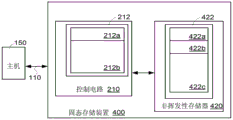
Referring to fig. 2, a solid-state storage device according to a first embodiment of the invention is shown. The solid-state storage device 200 includes: a control circuit 210 and a nonvolatile memory 220. The nonvolatile memory 220 is connected to the control circuit 210, and the nonvolatile memory 220 further includes a memory cell array (memory cell array) 222. Furthermore, the solid-state storage device 200 is connected to the host (host)150 via the external bus 110, wherein the external bus 110 can be a USB bus, a SATA bus, a PCIe bus, an m.2 bus, or an U.2 bus, etc.
The control circuit 210 includes a memory unit 212, and the memory unit 212 includes a first storage area 212a and a second storage area 212 b. After the control circuit 210 is manufactured, a boot code loader (boot code loader) is stored in the first storage area 212a to start the solid-state storage device 100. The first storage area 212a is a read-only storage area, and the boot program stored in the first storage area 212a does not disappear due to power failure.
In addition, the memory cell array 222 of the nonvolatile memory 220 includes a plurality of blocks (blocks), and each block includes a plurality of pages (pages). For example, there are 1024 blocks in the memory cell array 222, each block has 256 pages, and each page has a capacity of 16 Kbytes.
According to an embodiment of the present invention, the memory cell array 222 is configured with a third storage area 222a and a fourth storage area 222 b. The third storage area 222a is used for storing firmware programs, and the fourth storage area 222b is used for storing write data of the host 150. For example, 16 blocks of the memory cell array 222 are divided into a third storage area 222a for storing the firmware program, and the other 1008 blocks are divided into a fourth storage area 222b for storing the write data of the host 150. The firmware program is used to execute the operation of the solid-state storage device 100.
When the solid-state storage device 200 is loaded with power, the control circuit 210 first performs a start up procedure. During the boot-up procedure, the control circuit 210 executes the boot-up procedure in the first storage area 212a of the memory unit 212 and loads (loads) the firmware program of the third storage area 222a of the memory cell array 222 into the second storage area 212b of the memory unit 212 according to the boot-up procedure.
When the firmware program is loaded from the third storage area 222a to the second storage area 212b of the memory unit 212, the boot process is completed. At this time, the control circuit 210 can execute the firmware program in the second storage area 212b and make the solid-state storage device 200 operate normally.
When the solid state storage device 200 is operating normally, the control circuit 210 can operate according to a command issued by the host 150. For example, according to a write command issued by the host 150, the control circuit 210 stores the write data of the host 150 into the fourth storage area 222b of the memory cell array 222. Alternatively, according to a read command issued by the host 14, the control circuit 210 obtains read data from the fourth storage area 222b of the memory cell array 222 and transmits the read data to the host 150.
In addition, when the solid-state storage device 200 is powered off, the firmware program stored in the second storage area 212b of the memory unit 212 disappears. Therefore, when the solid-state storage device 200 receives power again and performs the boot process, the control circuit 210 executes the boot process in the first storage area 212a and reloads the firmware program in the third storage area 222a into the second storage area 212b of the memory unit 212 according to the boot process.
In the embodiment of the invention, the firmware program for executing the operation of the solid-state storage device 200 is stored in the non-volatile memory 220, rather than the read-only memory, so that the cost of the solid-state storage device can be effectively reduced. However, since the quality (quality) of the memory cell array 222 of the nonvolatile memory 220 gradually decreases with the use time, i.e., deteriorates, the firmware program may be damaged (collapse), and the firmware program cannot be read, so that the solid state storage device 200 cannot operate. Therefore, in the embodiment of the present invention, the firmware program is stored in the non-volatile memory 220 repeatedly in a large number. Specifically, in the third storage area 222a of the memory cell array 222, a binary code (binary code) of the firmware program is stored repeatedly in a large number. Thus, when the binary code of the firmware program in the third storage area 222a is damaged (collapse), the control circuit 210 can still successfully read the firmware program according to the content of the third storage area 222a and load the firmware program into the second storage area 212b of the control circuit 210.
Referring to FIG. 3A, a schematic diagram illustrating the storage of a firmware program in the third storage area 222a of the memory array 222 is shown. FIG. 3A illustrates 1024 blocks of the memory cell array 222, each block having 256 pages, and each page having a capacity of 16K bytes. Of course, the present invention is not limited thereto.
According to an embodiment of the present invention, in the third storage area 222a, 1 byte binary code in the firmware program is repeatedly stored in a space of one page. In other words, in the third storage area 222a, a binary code (byte) of 1 byte in the firmware program is stored in a space of one page. For example, assume that the firmware program size is 4Kbyte, i.e., the firmware program consists of 4K binaries. Therefore, the third storage area 222a needs to utilize 4K pages (pages) for storing the firmware program, and the capacity thereof is equal to 64Mbyte (4 K16 Kbyte). That is, the present invention stores the firmware program of 4Kbyte size in the third storage area 222a of 64Mbyte size.
According to an embodiment of the present invention, in order to ensure the correctness of the data in the third storage area 222a, a page space for storing 1 byte of binary code in the firmware program is divided into two parts. Wherein the bytes of the first portion of each page are used for repeatedly storing a binary code of the firmware program, and the bytes of the second portion of each page are used for repeatedly storing a complement of the binary code. Wherein the plurality of bytes of the first portion correspond to the plurality of bytes of the second portion, respectively.
As shown in FIG. 3A, each page is divided into two portions, the first portion having 8192 bytes (Byte [0]]~Byte[8191]) The second part has 8192 bytes (Byte 8192)]~Byte[16383]). Page 0(page0) stores the 0 th binary information of the firmware program, and the 0 th binary (FWb0) of the firmware program is repeatedly stored in the 8192 bytes of the first portion. In addition, the complement of the 0 th binary of the firmware program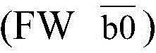 Is repeatedly stored in the second portion of 8192 bytes. For example, assume that the binary is "11001010" and the complement of the binary is "00110101".
Further, page 1(page1) stores the 1 st binary information of the firmware program. Therein, the 1 st binary (FW b1) of the firmware program is repeatedly stored in 8192 bytes of the first portion of page 1(page 1). In addition, the complement of the 1 st binary of the firmware program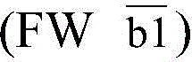 Is repeatedly stored at 8192 bytes of the second portion of page 1(page 1).
Similarly, page n (page n) stores the nth binary information of the firmware program. Wherein the nth binary (fwbn) of the firmware program is repeatedly stored in 8192 bytes of the first portion of page n (page n). In addition, the complement of the nth binary of the firmware program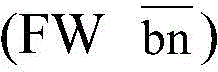 Is repeatedly stored in the second portion of page n (page n) 8192 bytes. And so on. In other words, according to the storage scheme of FIG. 3A, 4K binary codes of the firmware program are stored with a capacity of 4K pages (page 0-page 4095).
Referring to FIG. 3B, a flowchart of a firmware loading method according to the present invention is shown. The loading method of the firmware program is included in a boot code loader (bootcode loader). When the control circuit 210 executes the boot program during the boot process, the control circuit 210 loads (loads) the firmware program of the third storage area 222a of the memory cell array 222 into the second storage area 212b of the memory cell 212.
According to the embodiment of the invention, each page of the third storage area 222a stores one binary code information of the firmware program. Therefore, after each page of data is read, the control circuit 210 generates a binary code of the firmware program according to the binary code information and loads the binary code into the second storage area 212 b.
As shown in fig. 3B, data of one page is first read (step S302). That is, the control circuit 210 reads data of one page in the third storage area 222 a.
Next, one byte in the page is selected (step S304). Then, the contents of the selected byte and the corresponding byte are added to generate a result, and it is determined whether the result is "11111111111" (step S306). In step S304, the control circuit 210 may select one of the bytes in the first portion and find the corresponding byte in the second portion.
Taking FIG. 3A as an example, the first portion has 8192 bytes (Byte [0] Byte [8191]), and the second portion has 8192 bytes (Byte [8192] Byte [16383 ]). Wherein a first Byte (Byte [0]) of the first portion may correspond to a first Byte (Byte [8192]) of the second portion, a second Byte (Byte [1]) of the first portion may correspond to a second Byte (Byte [8193]) of the second portion, and so on. For example, in step S304, the control circuit 210 can select the first Byte (Byte [0]) of the first portion and can obtain the first Byte (Byte [8192]) corresponding to the second portion. Next, in step S306, the control circuit 210 adds the selected Byte (Byte [0]) and the content of the Byte (Byte [8192]) corresponding thereto to generate a result, and determines whether the added result is "11111111111".
Continuing with FIG. 3B, when the result is "11111111", it can be determined that the selected content of the byte is a binary code (binary code) in the firmware program. Then, the selected content of the byte is loaded into the second storage area 212b (step S310).
On the other hand, if the result of the addition is not "11111111", the content of the selected byte is incorrect and cannot be used as a binary code (binary code) of the firmware program. Therefore, another byte in the page is selected (step S308), and step 306 is performed again.
For example, after reading the data of page0, the control circuit 210 selects the 0 th Byte (Byte [0]) belonging to the first portion, obtains the content of the 0 th Byte (Byte [0]) as "11001010", obtains the content of the 8192 th Byte (Byte [8192]) corresponding to the second portion as "00110101", and obtains the result of the addition as "11111111". Therefore, the control circuit 210 uses the content "11001010" of the selected 0 th Byte (Byte [0]) as the 0 th binary code of the firmware program, and loads the content into the second storage area 212 b.
On the other hand, if any bit (bit) in the result of adding the 0 th Byte (Byte [0]) and the 8192 th Byte (Byte [8192]) has an error, the result of the addition will not be "11111111". At this time, the control circuit 210 selects another Byte belonging to the first portion, for example, the 1 st Byte (Byte [1]), and continues to determine whether the result of adding the 1 st Byte (Byte [1]) and the content of the 8193 th Byte (Byte [8193]) corresponding thereto in the second portion is "11111111111".
The present invention is not limited to the way of dividing one page into the first part and the second part. In another embodiment, the first portion and the second portion may be distinguished by parity. For example, Byte 0, Byte 2, Byte 4, and Byte … … in a page may be set as a first portion for repeatedly storing a binary code of a firmware program, and Byte 1, Byte 3, Byte 5, and Byte … … may be set as a second portion for repeatedly storing 1's complement of the binary code. Furthermore, the 0 th Byte (Byte [0]) may correspond to the 1 st Byte (Byte [1]), the 2 nd Byte (Byte [2]) may correspond to the 3 rd Byte (Byte [3]), and so on.
In order to prevent the memory cell array 222 from being degraded, the stored firmware program is damaged (collapse). The present invention uses a page space to repeatedly store the information of 1 binary code and its complement in the firmware program. Therefore, after the control circuit 210 reads the data of one page, it can add the selected byte and the corresponding byte to generate a result, and determine whether the added result is "11111111" as the basis for verifying whether the data is correct. Furthermore, since 1 binary code and its complement are repeatedly stored in the firmware program, different bytes can be selected for addition operation, wherein the binary code of 1 byte in the firmware program can be confirmed as long as one operation result is "11111111". Therefore, by using the storage method of the firmware program provided by the present invention, the control circuit 210 can still correctly load the binary code of the firmware program into the second storage area 212b when the memory cell array 222 is degraded.
Furthermore, fig. 3B only shows that 1 byte binary code in the firmware program is obtained from the binary code information in one page and loaded into the second storage area 212B. In other words, when the firmware program has 4K bytes (binary codes), the operation flow of fig. 3B needs to be performed for 4K pages (pages 0-page 4095) to obtain all 4K binary codes of the firmware program and load the obtained codes into the second storage area 212B.
The above embodiment is exemplified by a firmware program, but the invention is not limited thereto, and the firmware program can be a program or data stored in a nonvolatile memory and to be loaded into a memory unit in a control circuit. The following embodiment takes a configuration program (configuration program) as an example.
With the development of semiconductor technology, manufacturers of nonvolatile memories continue to push out new specifications of nonvolatile memories. Before the new specification of the non-volatile memory can be operated normally, it is necessary to accept configuration operation (configuration operation) issued by the control circuit. Otherwise, many errors are generated when reading and writing the nonvolatile memories with the new specification.
In a solid state storage device, a control circuit is required to perform a configuration operation on a new nonvolatile memory and to make the new nonvolatile memory operate correctly. The present invention provides a configuration program (configuration program) and stores it in a new non-volatile memory. When the solid-state storage device performs a boot procedure, the control circuit can load the configuration procedure and the firmware procedure into the control circuit. Then, the control circuit issues a configuration operation to the new non-volatile memory according to the configuration program. And then, the control circuit executes the firmware program to enable the solid-state storage device to normally operate.
Referring to fig. 4, a solid state storage device according to a second embodiment of the invention is shown. The solid-state storage device 400 includes: a control circuit 210 and a nonvolatile memory 420. The nonvolatile memory 420 is connected to the control circuit 210, and the nonvolatile memory 420 further includes a memory cell array 422. Moreover, the control circuit 210 is the same as the first embodiment, and is not described herein again.
According to an embodiment of the present invention, the memory cell array 422 is programmed with a third storage area 422a for storing configuration programs, a fourth storage area 422b for storing firmware programs, and a fifth storage area 422c for storing write data of the host 150. For example, 1 block of the memory cell array 422 is allocated as the third storage area 422a, 16 blocks are divided into the fourth storage area 422b, and the other 1007 blocks are divided into the fifth storage area 422 c.
When the solid-state storage device 400 receives power, the control circuit 210 first runs a start up procedure. During the boot process, the control circuit 210 executes the boot process in the first storage area 212a of the memory unit 212, and loads (loads) the configuration program of the third storage area 422a and the firmware program of the fourth storage area 422b of the memory cell array 222 into the second storage area 212b of the memory unit 212 according to the boot process.
When the configuration program and the firmware program are loaded from the third storage area 222a and the fourth storage area 222b into the second storage area 212b of the memory unit 212, the control circuit 210 first executes the configuration program in the second storage area 212b and performs the configuration operation on the non-volatile memory 420. Then, the control circuit 210 executes the firmware program to make the solid-state storage device 400 operate normally.
Furthermore, when the solid state storage device 400 operates normally, the control circuit 210 can operate according to a command issued by the host 150. For example, according to a write command issued by the host 150, the control circuit 210 stores write data of the host 150 into the fifth storage area 422c of the memory cell array 422. Alternatively, according to a read command issued by the host 14, the control circuit 210 obtains read data from the fifth storage area 422c of the memory cell array 224 and transmits the read data to the host 150.
In addition, when the solid-state storage device 400 is powered off, the firmware program stored in the second storage area 212b of the memory unit 212 disappears. Therefore, when the solid-state storage device 400 receives power again and performs the boot process, the control circuit 210 executes the boot process in the first storage area 212a and reloads the configuration program and the firmware program in the third storage area 422a and the fourth storage area 422b into the second storage area 212b of the memory unit 212 according to the boot process.
Referring to fig. 5A, a schematic diagram illustrating a configuration procedure in the third storage area 422a of the memory array 422 is shown. FIG. 5A illustrates 1024 blocks in the memory cell array 422, each block having 256 pages, and each page having a capacity of 16K bytes. Of course, the present invention is not limited thereto.
According to an embodiment of the present invention, in the third storage area 422a, 1 byte binary code (binary code) of the configuration program is repeatedly stored in a space of one page. In other words, in the third storage area 422a, 1 byte binary code (binary code) in the configuration program is stored in a space of one page. For example, assume that the configurator size is 265 bytes, i.e., the configurator consists of 256 bytes (bytes) of binary code. Therefore, the third storage area 422a needs to utilize 256 pages (pages) in total to store the firmware program, which has a capacity equal to 4Mbyte (256 × 16 Kbyte). That is, the present invention stores the allocation program of 256 bytes size in the third storage area 422a of 4 Mbytes size.
Similarly, to ensure the correctness of the data in the third storage area 422a, a page space for storing 1 byte of binary code in the configuration procedure is divided into two parts. Wherein the bytes of the first portion of each page are used for repeatedly storing a binary code of the configuration program, and the bytes of the second portion of each page are used for repeatedly storing a complement of the binary code. Wherein the plurality of bytes of the first portion correspond to the plurality of bytes of the second portion, respectively.
As shown in FIG. 5A, each page is divided into two portions, the first portion having 8192 bytes (Byte [0]]~Byte[8191]) The second part has 8192 bytes (Byte 8192)]~Byte[16383]). Page 0(page0) stores the 0 th binary information of the configuration program, and the 0 th binary (purpureb 0) of the configuration program is repeatedly stored in 8192 bytes of the first part. In addition, the complement of the 0 th binary of the configuration program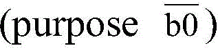 Is repeatedly stored in the second portion of 8192 bytes.
Further, page 1(page1) stores the 1 st binary information of the configuration program. Therein, the 1 st binary (payload b1) of the configurator program is repeatedly stored in 8192 bytes of the first portion of page 1(page 1). In addition, the 1 st binary's complement of the configuration program Is repeatedly stored at 8192 bytes of the second portion of page 1(page 1).
Furthermore, page m-1(page m-1) stores the (m-1) th binary code information of the configuration program. Wherein the first of the configuration procedurem-1 binary codes (purpose b1) are repeatedly stored in 8192 bytes of the first portion of page m-1(page m-1). In addition, the complement of the m-1 binary of the configuration program
 ) Is repeatedly stored in 8192 bytes of the second portion of page m-1(page m-1).
Page m (page m) stores the mth binary information of the firmware program. Wherein the mth binary (payload bm) of the configurator program is repeatedly stored in 8192 bytes of the first portion of page m (page m). In addition, the m-th binary complement of the program is configured Is repeatedly stored in the second portion of page m (page m) 8192 bytes. And so on.
Furthermore, according to the second embodiment of the present invention, the field in the configuration procedure includes a destination (purpose) field and a payload (payload) field. That is, the control circuit 210 issues the configuration operation to the nonvolatile memory 420 according to the binary codes of the destination field and the payload field.
Referring to FIG. 5B, a binary diagram of the binary and the complement of the destination field is shown. As shown in fig. 5B, when the binary code of the destination field is 0x43(01000011), the configuration operation of the control circuit 210 is to issue a command (command). When the binary code of the destination field is 0x41(01000001), the configuration operation of the control circuit 210 is the issue address (address). When the binary code of the destination field is 0x4F (01001111), the allocation operation of the control circuit 210 is the address offset (offset). When the binary code of the destination field is 0x57 (i.e., "01010111"), the configuration operation of the control circuit 210 is to sleep for a period of time (sleep in (ms)). When the binary code of the destination field is 0x70 (i.e., "01110000"), the configuration operation of the control circuit 210 is to perform comparison (compare).
For example, assume that the destination and payload fields are "01000011" and "11000101", respectively, when the control circuit 210 executes a configuration procedure. At this time, the configuration operation of the control circuit 210 is: issue an "11000101" instruction to non-volatile memory 420. Similarly, it is assumed that the destination and payload fields received by the control circuit 210 during the configuration procedure are "01011111" and "00001111", respectively. At this time, the configuration operation of the control circuit 210 indicates that the nonvolatile memory 420 enters the sleep state "00001111" milliseconds (ms).
Similarly, the configuration program of FIG. 5A can also be loaded into the second storage area 212B of the control circuit 210 by using the loading method of FIG. 3B.
The control circuit 210 reads the data of page 0(page0) in the third storage area 422 a. That is, the control circuit 210 reads data of one page in the third storage area 422 a.
Next, a byte in the page is selected. Then, the contents of the selected byte and the corresponding byte are added to generate a result, and whether the result is "11111111" is determined. That is, the control circuit 210 can select one of the bytes from the bytes of the first portion, find the corresponding byte in the bytes of the second portion, and add the contents of the two bytes.
When the result is "11111111", it can be confirmed that the content of the selected byte is a binary code (binary code) in the configurator. Then, the selected content of the byte is loaded into the second storage area 212b (step S310).
On the other hand, if the added result is not "11111111", the selected byte is represented by an error, and cannot be used as a binary code (binary code) of the configurator. Therefore, another byte in the page is selected to continue the above-described determination flow.
To prevent degradation of the memory cell array 422, this may lead to a corruption of the stored configuration program (collapse). The present invention uses a page space to repeatedly store 1 binary code and 1 complement of the binary code in the configuration program. Therefore, after the control circuit 210 reads the data of one page, it can add the selected byte and the corresponding byte to generate a result, and determine whether the added result is "11111111" as the basis for verifying whether the data is correct. Furthermore, since 1 binary code and its 1's complement are repeatedly stored in the configuration program, different bytes can be selected for addition, wherein the binary code of 1 byte in the configuration program can be confirmed as long as one operation result is "11111111". Therefore, by using the storage method of the configuration program proposed by the present invention, the control circuit 210 can still correctly load the binary code of the firmware program into the second storage area 212b when the memory cell array 422 is degraded.
In addition, the storage and loading manners of the firmware program of the solid-state storage device 400 according to the second embodiment of the invention are the same as those of the first embodiment, and are not described herein again.
As can be seen from the above description, the present invention provides a solid-state storage device and a method for loading related programs. In order to prevent the deterioration of the quality of the memory cell array, which leads to the destruction of the configuration program or firmware program stored in the memory cell array. The invention stores the binary code of the specific program repeatedly in a large number in the memory cell array, and the specific program can be a configuration program or a firmware program. When the binary code of part of the configuration program or part of the firmware program in the memory cell array is damaged (collapse), the control circuit can still successfully load the configuration program and the firmware program into the control circuit according to the content of the memory cell array.
Furthermore, in the disclosed technique, a binary message of the firmware program is stored in a page, and the page is divided into two parts, which respectively store the binary of the firmware program and the complement of the binary. It is to be understood that the present invention is not limited thereto, and those skilled in the art can appropriately modify the present invention to achieve the object of the present invention.
For example, two binary information of the firmware program can be stored in one page, and the page is divided into four parts, the first two parts respectively store the first binary of the firmware program and the complement of the first binary; the other two parts store the second binary code of the firmware program and the complement of the second binary code respectively. Similarly, the configuration program can also be stored in the memory cell array by the same storage method.
Furthermore, in the loading method of the firmware program, the control circuit adds the contents of each extracted byte of the first part and the second part of a page to obtain a result, and when the result is '11111111', the content of the bit extracted by the first part is confirmed to be a binary code of the firmware program. Of course, those skilled in the art can make modifications and achieve the objects of the invention.
For example, to further confirm the correctness of the binary code, the control circuit may add the first part and the second part of a page by taking out a byte of each of them and obtain a plurality of results, and when the results are all "11111111", the bit taken out by the first part is confirmed to be a binary code of the firmware program.
Although the present invention has been described with reference to the above embodiments, the embodiments are not intended to limit the present invention, and those skilled in the art can make modifications and improvements without departing from the spirit and scope of the present invention, so that the scope of the present invention is defined by the appended claims.
Claims (8)
1. A solid state storage device, comprising:
the control circuit comprises a storage unit, a control circuit and a control unit, wherein the storage unit comprises a first storage area and a second storage area, and the first storage area stores a starting program;
the nonvolatile memory is connected to the control circuit, wherein the nonvolatile memory is provided with a memory cell array, the memory cell array comprises a third storage area and a fourth storage area, the third storage area stores a specific program, and the control circuit controls the operation of the nonvolatile memory according to the specific program;
wherein the third storage area includes a first block, the first block includes a plurality of pages, and the first page of the first block is divided into a first portion and a second portion, the first portion of the first page includes a plurality of bytes repeatedly storing a first binary code of the specific program, and the second portion of the first page includes a plurality of bytes repeatedly storing a complement of the first binary code.
2. The solid state storage device of claim 1, wherein in the first block of the third storage area, a second page of the first block is divided into a first portion and a second portion, the first portion of the second page comprises a plurality of bytes repeatedly storing a second binary of the specific program, and the second portion of the second page comprises a plurality of bytes repeatedly storing a complement of the second binary.
3. The solid state storage device of claim 1, wherein when the control circuit executes the boot program, the control circuit reads the first page of the first block, obtains the first binary code of the specific program according to the content of the first page, and loads the first binary code into the second storage area of the control circuit.
4. The solid state storage device of claim 3, wherein the control circuitry selects a byte from the first portion of the first page and a corresponding byte from the second portion of the first page; the control circuit adds the selected content of the byte and the content of the corresponding byte to generate a result; when the result is "11111111", the control circuit takes the content of the selected byte as the first binary code of the specific program.
5. The solid state storage device of claim 1, wherein the specific program is a firmware program or a configuration program.
6. The solid state storage device of claim 1, wherein the memory cell array further comprises a fifth storage area, wherein the specific program stored in the third storage area is a firmware program, and the fourth storage area stores a configuration program, wherein the fourth storage area comprises a second block, the second block comprises a plurality of pages, and a third page of the second block is divided into a first portion and a second portion, the first portion of the third page comprises a plurality of bytes, is repeatedly stored with a first binary code of the configuration program, and the second portion of the third page comprises a plurality of bytes, is repeatedly stored with a complement of the first binary code of the configuration program.
7. The program loading method of the solid state storage device according to claim 6, comprising the steps of:
step 1, reading data in the first page in the first block of the third storage area;
step 2, selecting a byte from the first part of the first page and a corresponding byte from the second part of the first page, and adding the content of the selected byte and the content of the corresponding byte to generate a result; and
and 3, when the result is '11111111', taking the content of the selected byte as the first binary code and storing the first binary code in the second storage area of the control circuit.
8. The program loading method for a solid-state storage device according to claim 7, further comprising:
step 4, when the result is not "11111111", selecting another byte from the first part of the first page and another corresponding byte from the second part of the first page, and adding the content of the selected another byte and the content of the another corresponding byte to generate the result, and performing the step 3.
Priority Applications (2)
| Application Number | Priority Date | Filing Date | Title |
|---|---|---|---|
| CN201711181808.4A CN109828794B (en) | 2017-11-23 | 2017-11-23 | Solid state storage device and loading method of related program thereof |
| US15/872,004 US10379875B2 (en) | 2017-11-23 | 2018-01-16 | Solid state storage device and program loading method thereof |
Applications Claiming Priority (1)
| Application Number | Priority Date | Filing Date | Title |
|---|---|---|---|
| CN201711181808.4A CN109828794B (en) | 2017-11-23 | 2017-11-23 | Solid state storage device and loading method of related program thereof |
Publications (2)
| Publication Number | Publication Date |
|---|---|
| CN109828794A CN109828794A (en) | 2019-05-31 |
| CN109828794B true CN109828794B (en) | 2021-09-17 |
Family
ID=66532984
Family Applications (1)
| Application Number | Title | Priority Date | Filing Date |
|---|---|---|---|
| CN201711181808.4A Active CN109828794B (en) | 2017-11-23 | 2017-11-23 | Solid state storage device and loading method of related program thereof |
Country Status (2)
| Country | Link |
|---|---|
| US (1) | US10379875B2 (en) |
| CN (1) | CN109828794B (en) |
Citations (12)
| Publication number | Priority date | Publication date | Assignee | Title |
|---|---|---|---|---|
| US5497475A (en) * | 1993-02-05 | 1996-03-05 | National Semiconductor Corporation | Configurable integrated circuit having true and shadow EPROM registers |
| CN1485745A (en) * | 2003-08-08 | 2004-03-31 | 倚天资讯股份有限公司 | non-volatile memory access system and access method thereof |
| TW201005522A (en) * | 2008-07-24 | 2010-02-01 | Acer Inc | Computer system and storage-controlling method of the same |
| CN102157202A (en) * | 2008-01-22 | 2011-08-17 | 群联电子股份有限公司 | Method and Controller for Preventing Read Disturbance from Non-Volatile Memory |
| CN102915207A (en) * | 2011-08-01 | 2013-02-06 | 建兴电子科技股份有限公司 | Solid state storage device and data storage method thereof |
| TW201316341A (en) * | 2011-07-28 | 2013-04-16 | Sandisk Technologies Inc | Data recovery for defective word lines during programming of non-volatile memory arrays |
| CN103092771A (en) * | 2011-10-31 | 2013-05-08 | 建兴电子科技股份有限公司 | Solid state storage device and cache control method thereof |
| CN103123610A (en) * | 2011-11-18 | 2013-05-29 | 建兴电子科技股份有限公司 | Solid state storage device |
| CN103870215A (en) * | 2014-04-12 | 2014-06-18 | 天津瑞发科半导体技术有限公司 | USB solid-state disc firmware storage device |
| CN104461397A (en) * | 2014-12-19 | 2015-03-25 | 上海新储集成电路有限公司 | Solid-state drive and read-write method thereof |
| CN106569730A (en) * | 2015-10-08 | 2017-04-19 | 光宝电子(广州)有限公司 | Solid state device and relevant data writing method thereof |
| CN107092560A (en) * | 2016-02-17 | 2017-08-25 | 光宝电子(广州)有限公司 | Solid state storage device and apply to flash translation layer corresponding table method for reconstructing therein |
Family Cites Families (5)
| Publication number | Priority date | Publication date | Assignee | Title |
|---|---|---|---|---|
| US8380915B2 (en) * | 2010-01-27 | 2013-02-19 | Fusion-Io, Inc. | Apparatus, system, and method for managing solid-state storage media |
| JP2012123600A (en) * | 2010-12-08 | 2012-06-28 | Toshiba Corp | Memory system and memory controller |
| WO2014051611A1 (en) * | 2012-09-28 | 2014-04-03 | Duke University | Systems for and methods of extending lifetime of non-volatile memory |
| US10521339B2 (en) * | 2013-02-28 | 2019-12-31 | Technion Research And Development Foundation Ltd. | Retired page utilization (RPU) for improved write capacity of solid state drives |
| JP6073854B2 (en) | 2014-12-26 | 2017-02-01 | 京セラドキュメントソリューションズ株式会社 | Electronic equipment and firmware recovery program |
-
2017
- 2017-11-23 CN CN201711181808.4A patent/CN109828794B/en active Active
-
2018
- 2018-01-16 US US15/872,004 patent/US10379875B2/en active Active
Patent Citations (12)
| Publication number | Priority date | Publication date | Assignee | Title |
|---|---|---|---|---|
| US5497475A (en) * | 1993-02-05 | 1996-03-05 | National Semiconductor Corporation | Configurable integrated circuit having true and shadow EPROM registers |
| CN1485745A (en) * | 2003-08-08 | 2004-03-31 | 倚天资讯股份有限公司 | non-volatile memory access system and access method thereof |
| CN102157202A (en) * | 2008-01-22 | 2011-08-17 | 群联电子股份有限公司 | Method and Controller for Preventing Read Disturbance from Non-Volatile Memory |
| TW201005522A (en) * | 2008-07-24 | 2010-02-01 | Acer Inc | Computer system and storage-controlling method of the same |
| TW201316341A (en) * | 2011-07-28 | 2013-04-16 | Sandisk Technologies Inc | Data recovery for defective word lines during programming of non-volatile memory arrays |
| CN102915207A (en) * | 2011-08-01 | 2013-02-06 | 建兴电子科技股份有限公司 | Solid state storage device and data storage method thereof |
| CN103092771A (en) * | 2011-10-31 | 2013-05-08 | 建兴电子科技股份有限公司 | Solid state storage device and cache control method thereof |
| CN103123610A (en) * | 2011-11-18 | 2013-05-29 | 建兴电子科技股份有限公司 | Solid state storage device |
| CN103870215A (en) * | 2014-04-12 | 2014-06-18 | 天津瑞发科半导体技术有限公司 | USB solid-state disc firmware storage device |
| CN104461397A (en) * | 2014-12-19 | 2015-03-25 | 上海新储集成电路有限公司 | Solid-state drive and read-write method thereof |
| CN106569730A (en) * | 2015-10-08 | 2017-04-19 | 光宝电子(广州)有限公司 | Solid state device and relevant data writing method thereof |
| CN107092560A (en) * | 2016-02-17 | 2017-08-25 | 光宝电子(广州)有限公司 | Solid state storage device and apply to flash translation layer corresponding table method for reconstructing therein |
Non-Patent Citations (2)
| Title |
|---|
| H-ARC: A non-volatile memory based cache policy for solid state drives;Ziqi Fan等;《2014 30th Symposium on Mass Storage Systems and Technologies (MSST)》;20140717;第1-11页 * |
| 基于NAND非易失性闪存芯片的固态存储技术的应用及性能提升研究;董智刚;《中国优秀硕士学位论文全文数据库 (信息科技辑)》;20120815;第I137-25页 * |
Also Published As
| Publication number | Publication date |
|---|---|
| CN109828794A (en) | 2019-05-31 |
| US10379875B2 (en) | 2019-08-13 |
| US20190155612A1 (en) | 2019-05-23 |
Similar Documents
| Publication | Publication Date | Title |
|---|---|---|
| CN100377120C (en) | Control method of nonvolatile memory device | |
| CN106158038B (en) | Method for reading data from nonvolatile memory | |
| US10860247B2 (en) | Data writing method and storage controller | |
| CN102135891B (en) | System capable of realizing bootload, bootload control device and method | |
| CN100367306C (en) | non-volatile memory card | |
| US20100250875A1 (en) | Eeprom emulation using flash memory | |
| EP3834053B1 (en) | Power configuration component including selectable configuration profiles | |
| US8966344B2 (en) | Data protecting method, memory controller and memory storage device | |
| CN101727401A (en) | Link table recovery method | |
| US10509565B2 (en) | Apparatuses, methods, and computer-readable non-transitory recording mediums for erasure in data processing | |
| US11714656B2 (en) | Memory system executing loading of software at startup and control method | |
| CN103150184A (en) | Method for operating flash memory and system chip | |
| CN116185299A (en) | Flash memory controller and related apparatus and method | |
| EP3057100B1 (en) | Memory device and operating method of same | |
| CN100485810C (en) | Access method for logic nand flash memory chip and nand flash memory chip | |
| CN108108118B (en) | Data writing method and storage controller | |
| CN109828794B (en) | Solid state storage device and loading method of related program thereof | |
| CN110764947A (en) | Data writing method and storage controller | |
| CN119271460A (en) | A Linux dual-system startup and upgrade method, device, equipment and medium | |
| CN113590209B (en) | Chip starting control method, chip and electronic equipment | |
| US20200073590A1 (en) | Memory management method and storage controller | |
| US8214714B2 (en) | Nonvolatile storage device, controller of nonvolatile memory, and nonvolatile storage system | |
| CN100470681C (en) | A method of user program booting based on NAND flash memory | |
| CN117992081A (en) | Data storage device and firmware updating method | |
| CN117992082A (en) | Data storage device and firmware updating method |
Legal Events
| Date | Code | Title | Description |
|---|---|---|---|
| PB01 | Publication | ||
| PB01 | Publication | ||
| SE01 | Entry into force of request for substantive examination | ||
| SE01 | Entry into force of request for substantive examination | ||
| TA01 | Transfer of patent application right | ||
| TA01 | Transfer of patent application right |
Effective date of registration: 20200106 Address after: Room 302, factory a, No.8 Guangbao Road, Science City, Huangpu District, Guangzhou City, Guangdong Province Applicant after: Jianxing storage technology (Guangzhou) Co., Ltd Address before: 510663 No. 25 West spectral Road, Guangzhou hi tech Industrial Development Zone, Guangdong Applicant before: Guangbao Electronics (Guangzhou) Co., Ltd. Applicant before: Lite-On Technology Corporation |
|
| GR01 | Patent grant | ||
| GR01 | Patent grant |