CN109817679B - OLED display screen module - Google Patents
OLED display screen module Download PDFInfo
- Publication number
- CN109817679B CN109817679B CN201910095238.XA CN201910095238A CN109817679B CN 109817679 B CN109817679 B CN 109817679B CN 201910095238 A CN201910095238 A CN 201910095238A CN 109817679 B CN109817679 B CN 109817679B
- Authority
- CN
- China
- Prior art keywords
- oled display
- ultrasonic
- module
- sound
- layer
- Prior art date
- Legal status (The legal status is an assumption and is not a legal conclusion. Google has not performed a legal analysis and makes no representation as to the accuracy of the status listed.)
- Active
Links
Images


Classifications
-
- G—PHYSICS
- G10—MUSICAL INSTRUMENTS; ACOUSTICS
- G10K—SOUND-PRODUCING DEVICES; METHODS OR DEVICES FOR PROTECTING AGAINST, OR FOR DAMPING, NOISE OR OTHER ACOUSTIC WAVES IN GENERAL; ACOUSTICS NOT OTHERWISE PROVIDED FOR
- G10K11/00—Methods or devices for transmitting, conducting or directing sound in general; Methods or devices for protecting against, or for damping, noise or other acoustic waves in general
- G10K11/16—Methods or devices for protecting against, or for damping, noise or other acoustic waves in general
- G10K11/162—Selection of materials
-
- G—PHYSICS
- G06—COMPUTING OR CALCULATING; COUNTING
- G06V—IMAGE OR VIDEO RECOGNITION OR UNDERSTANDING
- G06V40/00—Recognition of biometric, human-related or animal-related patterns in image or video data
- G06V40/10—Human or animal bodies, e.g. vehicle occupants or pedestrians; Body parts, e.g. hands
- G06V40/12—Fingerprints or palmprints
- G06V40/13—Sensors therefor
- G06V40/1306—Sensors therefor non-optical, e.g. ultrasonic or capacitive sensing
-
- G—PHYSICS
- G10—MUSICAL INSTRUMENTS; ACOUSTICS
- G10K—SOUND-PRODUCING DEVICES; METHODS OR DEVICES FOR PROTECTING AGAINST, OR FOR DAMPING, NOISE OR OTHER ACOUSTIC WAVES IN GENERAL; ACOUSTICS NOT OTHERWISE PROVIDED FOR
- G10K11/00—Methods or devices for transmitting, conducting or directing sound in general; Methods or devices for protecting against, or for damping, noise or other acoustic waves in general
- G10K11/16—Methods or devices for protecting against, or for damping, noise or other acoustic waves in general
- G10K11/172—Methods or devices for protecting against, or for damping, noise or other acoustic waves in general using resonance effects
-
- H—ELECTRICITY
- H10—SEMICONDUCTOR DEVICES; ELECTRIC SOLID-STATE DEVICES NOT OTHERWISE PROVIDED FOR
- H10K—ORGANIC ELECTRIC SOLID-STATE DEVICES
- H10K59/00—Integrated devices, or assemblies of multiple devices, comprising at least one organic light-emitting element covered by group H10K50/00
-
- H—ELECTRICITY
- H10—SEMICONDUCTOR DEVICES; ELECTRIC SOLID-STATE DEVICES NOT OTHERWISE PROVIDED FOR
- H10K—ORGANIC ELECTRIC SOLID-STATE DEVICES
- H10K59/00—Integrated devices, or assemblies of multiple devices, comprising at least one organic light-emitting element covered by group H10K50/00
- H10K59/10—OLED displays
- H10K59/12—Active-matrix OLED [AMOLED] displays
-
- H—ELECTRICITY
- H10—SEMICONDUCTOR DEVICES; ELECTRIC SOLID-STATE DEVICES NOT OTHERWISE PROVIDED FOR
- H10K—ORGANIC ELECTRIC SOLID-STATE DEVICES
- H10K59/00—Integrated devices, or assemblies of multiple devices, comprising at least one organic light-emitting element covered by group H10K50/00
- H10K59/60—OLEDs integrated with inorganic light-sensitive elements, e.g. with inorganic solar cells or inorganic photodiodes
- H10K59/65—OLEDs integrated with inorganic image sensors
-
- H—ELECTRICITY
- H10—SEMICONDUCTOR DEVICES; ELECTRIC SOLID-STATE DEVICES NOT OTHERWISE PROVIDED FOR
- H10K—ORGANIC ELECTRIC SOLID-STATE DEVICES
- H10K59/00—Integrated devices, or assemblies of multiple devices, comprising at least one organic light-emitting element covered by group H10K50/00
- H10K59/80—Constructional details
- H10K59/8791—Arrangements for improving contrast, e.g. preventing reflection of ambient light
Landscapes
- Engineering & Computer Science (AREA)
- Multimedia (AREA)
- Physics & Mathematics (AREA)
- Acoustics & Sound (AREA)
- General Physics & Mathematics (AREA)
- Theoretical Computer Science (AREA)
- Human Computer Interaction (AREA)
- Chemical & Material Sciences (AREA)
- Inorganic Chemistry (AREA)
- Microelectronics & Electronic Packaging (AREA)
- Life Sciences & Earth Sciences (AREA)
- Sustainable Development (AREA)
- Electroluminescent Light Sources (AREA)
- Devices For Indicating Variable Information By Combining Individual Elements (AREA)
- Image Input (AREA)
Abstract
一种OLED显示屏模组,包括由上到下依次设置的盖板、第一胶粘剂、圆偏光片、OLED显示面板以及超声波指纹识别模块,所述超声波指纹识别模块位于所述OLED显示面板的下表面;所述OLED显示屏模组的两侧边设置有消声层,所述超声波指纹识别模块的两侧边设置有所述消声层,未与所述超声波指纹识别模块接触的部分所述OLED显示面板的下表面设置有所述消声层。有益效果:本发明所提供的OLED显示屏模组,在超声波指纹识别模块的两侧边以及OLED显示屏模组的两侧边上设置消声层,增强了超声波指纹识别模块的抗信号干扰能力,进一步提升了超声波指纹识别模块的传导效率。
An OLED display module, comprising a cover plate, a first adhesive, a circular polarizer, an OLED display panel and an ultrasonic fingerprint identification module arranged in sequence from top to bottom, the ultrasonic fingerprint identification module is located under the OLED display panel Surface; both sides of the OLED display module are provided with sound-absorbing layers, both sides of the ultrasonic fingerprint identification module are provided with the sound-absorbing layers, and the part not in contact with the ultrasonic fingerprint identification module is described The sound-absorbing layer is provided on the lower surface of the OLED display panel. Beneficial effects: The OLED display module provided by the present invention is provided with sound-absorbing layers on both sides of the ultrasonic fingerprint identification module and both sides of the OLED display module, which enhances the anti-signal interference capability of the ultrasonic fingerprint identification module. , which further improves the conduction efficiency of the ultrasonic fingerprint recognition module.
Description
技术领域technical field
本发明涉及显示技术领域,尤其涉及一种OLED显示屏模组。The invention relates to the field of display technology, in particular to an OLED display screen module.
背景技术Background technique
目前为了实现高的屏占比,一般将Home健虚拟化、屏幕唤醒解锁放置于显示区域,采用光学屏下指纹解锁的方法。但是光学指纹解锁具有下述问题:安全性不高,面对伪造的指纹信息,无法进行生物性活体判别。这不能满足当今用户注重保护个人隐私信息、解锁工具安全的需求。另外光学指纹识别对于光学信号有要求,所以手指的干净程度、显示屏整机的光学设计(反射率、透过率、亮度)等等是会影响识别效果的,用户体验不佳。At present, in order to achieve a high screen ratio, the Home key is generally virtualized and the screen wake-up and unlocking are placed in the display area, and the method of fingerprint unlocking under the optical screen is adopted. However, the optical fingerprint unlocking has the following problems: the security is not high, and in the face of forged fingerprint information, the biological living body cannot be discriminated. This cannot meet the needs of today's users who pay attention to protecting personal privacy information and unlocking tool security. In addition, optical fingerprint recognition has requirements for optical signals, so the cleanliness of the fingers, the optical design of the display (reflectivity, transmittance, brightness), etc. will affect the recognition effect, and the user experience is not good.
综上所述,现有的OLED显示屏模组,由于在运用屏下识别技术时,信号抗干扰性差且信号传播过程中衰减性强,进一步影响屏下识别模块的识别成功率。To sum up, the existing OLED display module, when using the off-screen recognition technology, has poor signal anti-interference and strong attenuation during signal propagation, which further affects the recognition success rate of the off-screen recognition module.
发明内容SUMMARY OF THE INVENTION
本发明提供一种OLED显示屏模组,能够提升屏下超声波识别模块的超声波传导效率,以解决现有的OLED显示屏模组,由于在运用屏下识别技术时,信号抗干扰性差且信号传播过程中衰减性强,进一步影响屏下识别模块的识别成功率的技术问题。The present invention provides an OLED display module, which can improve the ultrasonic conduction efficiency of the under-screen ultrasonic identification module, so as to solve the problem of the existing OLED display module, because when the under-screen identification technology is used, the signal has poor anti-interference and signal propagation. The attenuation is strong in the process, which further affects the technical problem of the recognition success rate of the recognition module under the screen.
为解决上述问题,本发明提供的技术方案如下:For solving the above problems, the technical solutions provided by the present invention are as follows:
本发明提供一种OLED显示屏模组,包括由上到下依次设置的盖板、第一胶粘剂、圆偏光片、OLED显示面板以及超声波指纹识别模块,所述超声波指纹识别模块位于所述OLED显示面板的下表面;所述OLED显示屏模组的两侧边设置有消声层,所述超声波指纹识别模块的两侧边设置有所述消声层,未与所述超声波指纹识别模块接触的部分所述OLED显示面板的下表面设置有所述消声层。The present invention provides an OLED display module, comprising a cover plate, a first adhesive, a circular polarizer, an OLED display panel and an ultrasonic fingerprint identification module arranged in order from top to bottom, wherein the ultrasonic fingerprint identification module is located on the OLED display. The lower surface of the panel; the two sides of the OLED display module are provided with sound-absorbing layers, and the two sides of the ultrasonic fingerprint identification module are provided with the sound-absorbing layers, and those not in contact with the ultrasonic fingerprint identification module Part of the lower surface of the OLED display panel is provided with the sound-absorbing layer.
根据本发明一优选实施例,所述第一胶粘剂为OCA胶(固态透明光学胶),所述消声层为消声瓦材料,所述消声瓦材料包括丁苯橡胶、聚氨脂、玻璃纤维、聚硫橡胶以及硅胶中的任意一种。According to a preferred embodiment of the present invention, the first adhesive is OCA glue (solid transparent optical glue), the sound-absorbing layer is a sound-absorbing tile material, and the sound-absorbing tile material includes styrene-butadiene rubber, polyurethane, glass Any of fiber, polysulfide rubber and silicone.
根据本发明一优选实施例,所述超声波指纹识别模块包括超声波识别传感器,所述超声波识别传感器能够发射一定频率的超声波。According to a preferred embodiment of the present invention, the ultrasonic fingerprint recognition module includes an ultrasonic recognition sensor, and the ultrasonic recognition sensor can emit ultrasonic waves of a certain frequency.
根据本发明一优选实施例,所述消声层的阻抗匹配所述超声波识别传感器发出的超声波对应的频率。。According to a preferred embodiment of the present invention, the impedance of the sound-absorbing layer matches the frequency corresponding to the ultrasonic waves emitted by the ultrasonic identification sensor. .
根据本发明一优选实施例,所述OLED显示面板的下表面与所述超声波指纹识别模块的顶面贴附,所述超声波指纹识别模块的两侧边分别通过第二胶粘剂内嵌于背板以及第一泡棉层的内部,所述超声波指纹识别模块的底面与第二泡棉层贴附。According to a preferred embodiment of the present invention, the lower surface of the OLED display panel is attached to the top surface of the ultrasonic fingerprint identification module, and the two sides of the ultrasonic fingerprint identification module are respectively embedded in the back plate and the back plate through the second adhesive. Inside the first foam layer, the bottom surface of the ultrasonic fingerprint identification module is attached to the second foam layer.
根据本发明一优选实施例,所述第一泡棉层的上下表面以及所述第二泡棉层的上下表面均设置有所述消声层,所述第一泡棉层以及所述第二泡棉层均为全闭孔的发泡体。According to a preferred embodiment of the present invention, the upper and lower surfaces of the first foam layer and the upper and lower surfaces of the second foam layer are provided with the sound-absorbing layer, the first foam layer and the second The foam layers are all closed-cell foams.
根据本发明一优选实施例,所述第二胶粘剂包括紫外光固化胶、橡胶、硅胶以及玻璃胶中的任意一种;所述第二胶粘剂的胶体呈倒梯形,所述第二胶粘剂的胶体与所述OLED显示面板的下表面的接触角大于90°。According to a preferred embodiment of the present invention, the second adhesive comprises any one of UV-curable adhesive, rubber, silica gel and glass adhesive; the colloid of the second adhesive is in the shape of an inverted trapezoid, and the colloid of the second adhesive is in the shape of an inverted trapezoid. The contact angle of the lower surface of the OLED display panel is greater than 90°.
根据本发明一优选实施例,所述超声波指纹识别模块的两侧边与所述第二胶粘剂的胶体之间的接触部位上设置有凹凸结构。According to a preferred embodiment of the present invention, a concave-convex structure is provided on the contact portion between the two sides of the ultrasonic fingerprint identification module and the colloid of the second adhesive.
根据本发明一优选实施例,所述OLED显示面板包括TFT阵列基板、OLED发光层、阳极金属层、阴极金属层以及封装膜层,所述超声波指纹识别模块包括超声波识别传感器,所述超声波识别传感器在空间上与所述TFT阵列基板中的平坦化层上下位置关系垂直重叠。According to a preferred embodiment of the present invention, the OLED display panel includes a TFT array substrate, an OLED light-emitting layer, an anode metal layer, a cathode metal layer, and an encapsulation film layer, and the ultrasonic fingerprint identification module includes an ultrasonic identification sensor, and the ultrasonic identification sensor In space, it vertically overlaps with the upper and lower positional relationship of the planarization layer in the TFT array substrate.
根据本发明一优选实施例,所述超声波识别传感器的感应面为整面式,所述超声波识别传感器贴附于所述OLED显示面板的下表面,相邻两所述超声波识别传感器之间通过所述消声层粘结。According to a preferred embodiment of the present invention, the sensing surface of the ultrasonic recognition sensor is a full-surface type, the ultrasonic recognition sensor is attached to the lower surface of the OLED display panel, and two adjacent ultrasonic recognition sensors pass through each other. The sound-absorbing layer is bonded.
本发明的有益效果为:本发明所提供的OLED显示屏模组,在超声波指纹识别模块的两侧边以及OLED显示屏模组的两侧边上设置消声层,增强了超声波指纹识别模块的抗信号干扰能力,进一步提升了超声波指纹识别模块的传导效率。The beneficial effects of the present invention are: in the OLED display module provided by the present invention, sound-absorbing layers are arranged on both sides of the ultrasonic fingerprint identification module and on both sides of the OLED display module, which enhances the performance of the ultrasonic fingerprint identification module. The anti-signal interference ability further improves the conduction efficiency of the ultrasonic fingerprint identification module.
附图说明Description of drawings
为了更清楚地说明实施例或现有技术中的技术方案,下面将对实施例或现有技术描述中所需要使用的附图作简单介绍,显而易见地,下面描述中的附图仅仅是发明的一些实施例,对于本领域普通技术人员来讲,在不付出创造性劳动的前提下,还可以根据这些附图获得其他的附图。In order to more clearly illustrate the embodiments or technical solutions in the prior art, the following briefly introduces the accompanying drawings that are used in the description of the embodiments or the prior art. Obviously, the drawings in the following description are only for invention. In some embodiments, for those of ordinary skill in the art, other drawings can also be obtained according to these drawings without any creative effort.
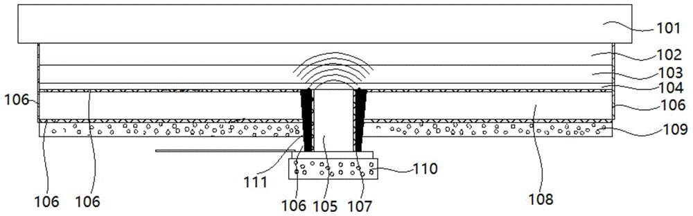
图1为本发明OLED显示屏模组实施例一截面结构示意图。FIG. 1 is a schematic cross-sectional structural diagram of an embodiment of an OLED display module according to the present invention.
图2为本发明OLED显示屏模组实施例二局部截面结构示意图。FIG. 2 is a partial cross-sectional structural diagram of the second embodiment of the OLED display module of the present invention.
图3为本发明OLED显示屏模组实施例三截面结构示意图。FIG. 3 is a schematic cross-sectional structural diagram of Embodiment 3 of the OLED display module of the present invention.
具体实施方式Detailed ways
以下各实施例的说明是参考附加的图示,用以例示本发明可用以实施的特定实施例。本发明所提到的方向用语,例如[上]、[下]、[前]、[后]、[左]、[右]、[内]、[外]、[侧面]等,仅是参考附加图式的方向。因此,使用的方向用语是用以说明及理解本发明,而非用以限制本发明。在图中,结构相似的单元是用以相同标号表示。The following descriptions of the various embodiments refer to the accompanying drawings to illustrate specific embodiments in which the invention may be practiced. The directional terms mentioned in the present invention, such as [up], [down], [front], [rear], [left], [right], [inner], [outer], [side], etc., are only for reference Additional schema orientation. Therefore, the directional terms used are for describing and understanding the present invention, not for limiting the present invention. In the figures, structurally similar elements are denoted by the same reference numerals.
本发明针对现有的OLED显示屏模组,由于在运用屏下识别技术时,信号抗干扰性差且信号传播过程中衰减性强,进一步影响屏下识别模块的识别成功率的技术问题,本实施例能够解决该缺陷。The present invention aims at the technical problem of the existing OLED display module, which further affects the identification success rate of the under-screen identification module due to poor signal anti-interference and strong attenuation in the process of signal propagation when the under-screen identification technology is used. example can solve this defect.
实施例一:Example 1:
如图1所示,为本发明OLED显示屏模组实施例一截面结构示意图。其中,本发明提供一种OLED显示屏模组,包括由上到下依次设置的盖板101、第一胶粘剂102、圆偏光片103、OLED显示面板104以及超声波指纹识别模块105,所述超声波指纹识别模块105位于所述OLED显示面板104的下表面;As shown in FIG. 1 , it is a schematic cross-sectional structure diagram of an embodiment of an OLED display module of the present invention. Among them, the present invention provides an OLED display module, including a
其中,所述OLED显示屏模组的两侧边设置有消声层106,所述超声波指纹识别模块105的两侧边设置有所述消声层106,未与所述超声波指纹识别模块接触的部分所述OLED显示面板的下表面104设置有所述消声层106。Wherein, the two sides of the OLED display module are provided with sound-absorbing
具体的,所述OLED显示面板104的下表面与所述超声波指纹识别模块105的顶面贴附,所述超声波指纹识别模块105的两侧边分别通过第二胶粘剂107内嵌于背板108以及第一泡棉层109的内部,所述超声波指纹识别模块105的底面与第二泡棉层110贴附。Specifically, the lower surface of the
具体的,所述第一泡棉层109的上下表面以及所述第二泡棉层110的上下表面均设置有所述消声层106,所述第一泡棉层109以及所述第二泡棉层110均为全闭孔的发泡体。Specifically, the upper and lower surfaces of the
其中,所述第一胶粘剂102为OCA胶(固态透明光学胶)。所述消声层106可以采用军用潜艇所采用的消声瓦材料,比喻丁苯橡胶、聚氨脂、玻璃纤维、聚硫橡胶、硅胶等柔软的多孔材料。所述超声波指纹识别模块105包括超声波识别传感器,所述超声波识别传感器能够发射一定频率的超声波。所述消声层106的阻抗匹配所述超声波识别传感器发出的超声波对应的频率。Wherein, the
具体的,所述第二胶粘剂107包括紫外光固化胶、橡胶、硅胶以及玻璃胶中的任意一种;所述第二胶粘剂107的胶体呈倒梯形,所述第二胶粘剂107的胶体与所述OLED显示面板的下表面104的接触角大于90°。Specifically, the
具体的,所述超声波指纹识别模块105的两侧边与所述第二胶粘剂107的胶体之间的接触部位上设置有凹凸结构。Specifically, a concave-convex structure is provided on the contact portion between the two sides of the ultrasonic
本发明OLED显示屏模组实施例一的所述超声波指纹识别模块105采用模块式的模组单元,所述超声波指纹识别模块105内嵌于显示模组背部,采用封胶的方法贴附于所述OLED显示面板104的下表面,所述超声波指纹识别模块105与所述OLED显示面板104之间不允许有气泡和异物,在负压的环境下使用所述第二胶粘剂107进行封胶。所述第二胶粘剂107的胶体呈现倒梯形设计,保证与所述OLED显示面板104的接触角大于90°,同时在与所述第二胶粘剂107的胶体接触的部位留有凹凸结构111,这样的设计能够保护所述OLED显示面板104不会受到来自所述超声波指纹识别模块105背部的刺伤应力,增加粘结强度,同时也能实现所述超声波指纹识别模块105与所述OLED显示面板104之间的界面上不会残留空气层。在保证缓冲性能良好的前提下,采用全闭孔发泡的方式的所述第一泡棉层109对于来自显示屏背部(手机中框)的干扰声波也会产生阻尼和过滤的效果。为了增加保护,在所述超声波指纹识别模块105的背部增加一层所述第二泡棉层110。The ultrasonic
本发明OLED显示屏模组实施例一的显示模组的侧边、所述OLED显示面板104的下表面、所述超声波指纹识别模块105的侧边、所述第一泡棉层109以及所述第二泡棉层110的上下表面等部位均已经进行消声材料的涂布或者贴附。主要原因是超声波可以在显示屏模组内部不同方向上进行反射和传导,包括外部(显示屏外界环境、手机侧边和中框等)传导内部的超声波信号,从而对于指纹识别模块的信号(超声波)的发射、接受、识别产生影响。所述消声层106可以过滤掉干扰信号,对于显示屏模组内部不必要的超声波进行吸收和消声。当声波进入所述消声层106中时,一部分声能在多孔材料的孔隙中摩擦而转化成热能耗散掉,使通过消声器的声波减弱。消声一般是要求阻抗匹配,让声音进入某一介质利用阻尼把声音吸收。吸声材料一般有消声海绵、微穿孔结构等,常用的结构就是尖劈内置消声海绵结构,其他利用具有阻尼的共振腔结构也能很好的消声。The side of the display module, the lower surface of the
实施例二:Embodiment 2:
如图2所示,为本发明OLED显示屏模组实施例二局部截面结构示意图。其与实施例一的不同之处仅在于超声波指纹识别模块25与所述OLED显示面板的下表面的贴附位置不同;其中,所述OLED显示面板包括TFT阵列基板20、OLED发光层21、阳极金属层22、阴极金属层23以及封装膜层24;所述超声波指纹识别模块25包括超声波识别传感器,所述超声波识别传感器在空间上与所述TFT阵列基板20中的平坦化层208上下位置关系垂直重叠,即所述超声波识别传感器的顶面与所述OLED显示面板的下表面的贴附位置避开了所述OLED显示面板的像素开孔区域。As shown in FIG. 2 , it is a schematic diagram of a partial cross-sectional structure of the second embodiment of the OLED display module of the present invention. The only difference from the first embodiment is that the ultrasonic
具体的,所述TFT阵列基板20包括柔性基板201、缓冲层202、有源层203、栅极绝缘层204、栅极金属层205、层间绝缘层206、源漏极金属层207、平坦化层208以及像素限定层209;其中,所述源漏极金属层207通过第一通孔210以及第二通孔211与所述有源层相连通,所述阳极金属层23通过第三通孔212与所述源漏极金属层207相连通。Specifically, the TFT array substrate 20 includes a
本发明OLED显示屏模组实施例二将所述超声波识别传感器的顶面与所述OLED显示面板的下表面的贴附位置避开了所述OLED显示面板的像素开孔区域,能够增加超声波信号在所述OLED显示面板内部的传导,防止信号的弥散和减弱。In the second embodiment of the OLED display module of the present invention, the attachment position of the top surface of the ultrasonic recognition sensor and the lower surface of the OLED display panel avoids the pixel opening area of the OLED display panel, which can increase the ultrasonic signal Conduction inside the OLED display panel prevents signal dispersion and weakening.
实施例三:Embodiment three:
如图3所示,为本发明OLED显示屏模组实施例三截面结构示意图。其与实施例一以及实施例二的不同之处仅在于所述超声波指纹识别模块31的绑定方式的不同;其中,所述超声波指纹识别模块31包括超声波识别传感器311,所述超声波识别传感器311的感应面为整面式,所述超声波识别传感器311贴附于所述OLED显示面板21的下表面,相邻两所述超声波识别传感器311之间通过消声层32粘结。As shown in FIG. 3 , it is a schematic cross-sectional structure diagram of Embodiment 3 of the OLED display module of the present invention. The difference between it and Embodiment 1 and Embodiment 2 is only in that the binding method of the ultrasonic
本发明的有益效果为:本发明所提供的OLED显示屏模组,在超声波指纹识别模块的两侧边以及OLED显示屏模组的两侧边上设置消声层,增强了超声波指纹识别模块的抗信号干扰能力,进一步提升了超声波指纹识别模块的传导效率。The beneficial effects of the present invention are: in the OLED display module provided by the present invention, sound-absorbing layers are arranged on both sides of the ultrasonic fingerprint identification module and on both sides of the OLED display module, which enhances the performance of the ultrasonic fingerprint identification module. The anti-signal interference ability further improves the conduction efficiency of the ultrasonic fingerprint identification module.
综上所述,虽然本发明已以优选实施例揭露如上,但上述优选实施例并非用以限制本发明,本领域的普通技术人员,在不脱离本发明的精神和范围内,均可作各种更动与润饰,因此本发明的保护范围以权利要求界定的范围为准。In summary, although the present invention has been disclosed above with preferred embodiments, the above preferred embodiments are not intended to limit the present invention. Those of ordinary skill in the art can make various Therefore, the protection scope of the present invention is subject to the scope defined by the claims.
Claims (8)
Priority Applications (3)
| Application Number | Priority Date | Filing Date | Title |
|---|---|---|---|
| CN201910095238.XA CN109817679B (en) | 2019-01-31 | 2019-01-31 | OLED display screen module |
| PCT/CN2019/078136 WO2020155321A1 (en) | 2019-01-31 | 2019-03-14 | Oled display screen module |
| US16/478,044 US11315356B2 (en) | 2019-01-31 | 2019-03-14 | Organic light emitting diode display panel module |
Applications Claiming Priority (1)
| Application Number | Priority Date | Filing Date | Title |
|---|---|---|---|
| CN201910095238.XA CN109817679B (en) | 2019-01-31 | 2019-01-31 | OLED display screen module |
Publications (2)
| Publication Number | Publication Date |
|---|---|
| CN109817679A CN109817679A (en) | 2019-05-28 |
| CN109817679B true CN109817679B (en) | 2020-10-16 |
Family
ID=66606078
Family Applications (1)
| Application Number | Title | Priority Date | Filing Date |
|---|---|---|---|
| CN201910095238.XA Active CN109817679B (en) | 2019-01-31 | 2019-01-31 | OLED display screen module |
Country Status (3)
| Country | Link |
|---|---|
| US (1) | US11315356B2 (en) |
| CN (1) | CN109817679B (en) |
| WO (1) | WO2020155321A1 (en) |
Families Citing this family (1)
| Publication number | Priority date | Publication date | Assignee | Title |
|---|---|---|---|---|
| CN110263734B (en) * | 2019-06-25 | 2021-08-17 | 昆山国显光电有限公司 | Fingerprint module and display device |
Family Cites Families (13)
| Publication number | Priority date | Publication date | Assignee | Title |
|---|---|---|---|---|
| JP2003241897A (en) * | 2002-02-15 | 2003-08-29 | Hitachi Printing Solutions Ltd | Touch panel |
| US9815087B2 (en) | 2013-12-12 | 2017-11-14 | Qualcomm Incorporated | Micromechanical ultrasonic transducers and display |
| KR20170041010A (en) * | 2015-10-06 | 2017-04-14 | 삼성전기주식회사 | Printed circuit board for fingerprint sensor, fingerprint sensor and manufacturing method of printed circuit board for fingerprint sensor |
| US11003884B2 (en) * | 2016-06-16 | 2021-05-11 | Qualcomm Incorporated | Fingerprint sensor device and methods thereof |
| US10741621B2 (en) * | 2016-11-25 | 2020-08-11 | Lg Display Co., Ltd. | Display device with a fingerprint sensor |
| CN106951887B (en) * | 2017-04-25 | 2020-07-03 | 太原科技大学 | Microcapacitive ultrasonic transducer linear array device for identification |
| CN107170360B (en) * | 2017-04-27 | 2020-03-24 | Oppo广东移动通信有限公司 | Display screen, preparation method thereof and mobile terminal |
| US20180373913A1 (en) * | 2017-06-26 | 2018-12-27 | Qualcomm Incorporated | Ultrasonic fingerprint sensor for under-display applications |
| CN107527020A (en) * | 2017-07-31 | 2017-12-29 | 广东欧珀移动通信有限公司 | Biometric methods and related products |
| CN207182304U (en) * | 2017-09-12 | 2018-04-03 | 南昌欧菲生物识别技术有限公司 | Electronic equipment |
| CN207182303U (en) * | 2017-09-12 | 2018-04-03 | 南昌欧菲生物识别技术有限公司 | Ultrasonic wave biological identification device and electronic equipment |
| KR102576093B1 (en) * | 2018-02-14 | 2023-09-11 | 삼성디스플레이 주식회사 | Biometric information sensor and display device having the same |
| KR20200075208A (en) * | 2018-12-17 | 2020-06-26 | 삼성디스플레이 주식회사 | Display device |
-
2019
- 2019-01-31 CN CN201910095238.XA patent/CN109817679B/en active Active
- 2019-03-14 US US16/478,044 patent/US11315356B2/en active Active
- 2019-03-14 WO PCT/CN2019/078136 patent/WO2020155321A1/en not_active Ceased
Also Published As
| Publication number | Publication date |
|---|---|
| US20210357602A1 (en) | 2021-11-18 |
| CN109817679A (en) | 2019-05-28 |
| WO2020155321A1 (en) | 2020-08-06 |
| US11315356B2 (en) | 2022-04-26 |
Similar Documents
| Publication | Publication Date | Title |
|---|---|---|
| CN109817679B (en) | OLED display screen module | |
| CN104966511A (en) | Binary embedded cylinder cavity sound absorption covering layer | |
| US12427749B2 (en) | Glass plate structure, diaphragm, and opening member | |
| CN110047392A (en) | A kind of display device | |
| US20240184333A1 (en) | Electronic device | |
| CN105006226A (en) | Cylindrical cavity combination sound-absorbing coating | |
| CN206928450U (en) | A kind of sound insulating sheet material for building | |
| CN205647996U (en) | Ultrasonic bonding glue overflow -prevention structure | |
| CN110183993A (en) | Screen protecting film and electronic equipment | |
| CN201025488Y (en) | Composite sonar deflector shell plate | |
| CN114516259B (en) | Window glass and vehicle | |
| CN204926787U (en) | Combined sound absorption overburden of cylindrical cavity | |
| CN205487329U (en) | Pad pasting of making an uproar falls | |
| CN108824761A (en) | A kind of steady type PVC floor | |
| CN109164622B (en) | Terminal panel and mobile terminal | |
| TWI634013B (en) | Electronic device with protective layer | |
| CN211447932U (en) | Mute room for detecting air conditioner component | |
| CN213383428U (en) | Accuse glass in energy-saving with dustproof construction | |
| CN210234268U (en) | Composite sound insulation film | |
| CN108505641A (en) | A kind of novel wedge absorber | |
| CN219652928U (en) | Toughened film with buffer function | |
| CN207264692U (en) | Vehicle-carrying display screen with explosion prevention function | |
| CN208180436U (en) | Anti-glare mobile phone cover glass | |
| CN214881220U (en) | A mobile phone tempered film with edge and corner protection function | |
| CN207182331U (en) | Ultrasonic fingerprint identifies module and electronic equipment |
Legal Events
| Date | Code | Title | Description |
|---|---|---|---|
| PB01 | Publication | ||
| PB01 | Publication | ||
| SE01 | Entry into force of request for substantive examination | ||
| SE01 | Entry into force of request for substantive examination | ||
| GR01 | Patent grant | ||
| GR01 | Patent grant |