Disclosure of Invention
The application provides a spliced display panel, a display device and a driving method, which can solve the problems of complex installation and high cost of an LED lamp bar in the related technology. The technical scheme is as follows:
on one hand, the optical compensation strip is applied to a spliced display panel, is positioned on the light emergent surfaces of two adjacent sub-display panels in the spliced display panel, and covers the splicing seams of the two adjacent sub-display panels;
the optical compensation strip includes: the display cover plate is fixed on the light emergent surfaces of the two adjacent sub-display panels, and the at least two prisms are positioned between the display cover plate and the light emergent surfaces;
a gap exists between each prism and the display cover plate, and each prism, the display cover plate and the splicing seam extend along a first direction;
the at least two prisms are used for refracting light rays emitted by the two adjacent sub-display panels to an area corresponding to the splicing seam on the display cover plate.
Optionally, the at least two prisms include: the light-emitting device comprises a first prism and a second prism which are adjacent, wherein the intersection line of the first prism and the second prism is collinear with the central axis of the splicing seam in the orthographic projection of the light-emitting surface, and the central axis is parallel to the first direction.
Optionally, the orthographic projection of the side surface of the first prism, which is far away from the second prism, on the light exit surface is located in a display area of a first sub-display panel of the two adjacent sub-display panels, and is used for refracting light emitted by the first sub-display panel to an area, corresponding to the seam, on the display cover plate;
the side face, far away from the first prism, of the second prism is located in the display area of the second sub-display panel in the two adjacent sub-display panels in the orthographic projection of the light-emitting face, and the second prism is used for refracting light emitted by the second sub-display panel to the area, corresponding to the splicing seam, on the display cover plate.
Optionally, the side of the first prism far away from the second prism and the maximum included angle of the light emitting surface, and the side of the second prism far away from the first prism and the maximum included angle of the light emitting surface are both smaller than a first critical angle δ, and the first critical angle δ satisfies: δ ═ arcsin (n2/n 1);
wherein n1 is a refractive index of the first prism, n2 is a refractive index of a medium between the first prism and the display cover, and a refractive index of the second prism is equal to a refractive index of the first prism.
Optionally, a distance between the first prism and the display cover plate is greater than or equal to a first distance, and the first distance satisfies: h1=d0/(2×tanα1);
The distance between the second prism and the display cover plate is larger than or equal to a second distance, and the second distance satisfies the following conditions: h2=d0/(2×tanα2);
Wherein d is0The length of the abutted seam along a second direction;
α 1 satisfies: α 1 ═ arcsin [ (n1/n2) × sin θ 1max]-θ1max;
α 2 satisfies: α 2 ═ arcsin [ (n1/n2) × sin θ 2max]-θ2max;
θ1maxThe side surface of the first prism far away from the second prism and the light-emitting surfaceMaximum angle of (e 2)maxThe maximum included angle between the side face of the second prism far away from the first prism and the light-emitting face is set;
the second direction is perpendicular to the first direction, and the first direction and the second direction are both parallel to the light emitting surface.
Optionally, the side surface of the first prism close to the second prism and the side surface of the second prism close to the first prism are both used for totally reflecting the light at the seam;
the distance between the edge of the first prism, which is close to the display cover plate and extends along the first direction, and the edge of the second prism, which is close to the display cover plate and extends along the first direction, is equal to the length of the splicing seam along the second direction;
the second direction is perpendicular to the first direction, and the first direction and the second direction are both parallel to the light emitting surface.
Optionally, the side of the first prism close to the second prism and the included angle of the light emitting surface, and the side of the second prism close to the first prism and the included angle of the light emitting surface are both greater than or equal to a first critical angle δ, and the first critical angle δ satisfies: δ ═ arcsin (n2/n 1);
wherein n1 is a refractive index of the first prism, n2 is a refractive index of a medium between the first prism and the display cover, and a refractive index of the second prism is equal to a refractive index of the first prism.
Optionally, the at least two prisms further include: at least one third prism and at least one fourth prism;
the at least one third prism is arranged on one side of the first prism far away from the second prism, and the at least one fourth prism is arranged on one side of the second prism far away from the first prism;
the orthographic projection of each third prism on the light emitting surface is positioned in a display area of a first sub-display panel in the two adjacent sub-display panels and used for refracting light rays emitted by the first sub-display panel to an area, corresponding to the splicing seam, on the display cover plate;
and the orthographic projection of each fourth prism on the light-emitting surface is positioned in a display area of a second sub-display panel in the two adjacent sub-display panels and is used for refracting light rays emitted by the second sub-display panel to an area, corresponding to the splicing seam, on the display cover plate.
Optionally, the optical compensation strip further includes: a prism substrate;
the prism base material and the display cover plate are fixed on the light-emitting surfaces of the two adjacent sub-display panels, one side of the prism base material is in contact with the light-emitting surfaces, and the other side of the prism base material is in contact with the display cover plate;
the display cover plate comprises a prism base material and a display cover plate, wherein one side of the prism base material, which is in contact with the display cover plate, is also provided with a first groove, the at least two prisms are arranged in the first groove, and the first groove extends along the first direction.
Optionally, a second groove is formed in one side, away from the display cover plate, of the prism substrate, the second groove extends along the first direction, an orthogonal projection of an axis of the second groove on the light emitting surface is collinear with a central axis of the splice, and the axis and the central axis are both parallel to the first direction;
the difference value between the sum of the lengths of the frames at the splicing positions of the two adjacent sub-display panels along the second direction and the length of the second groove along the second direction is smaller than a threshold value, the second direction is perpendicular to the first direction, and the first direction and the second direction are parallel to the light emitting surface.
Optionally, the length of one side of the prism base material, which is close to the display cover plate, along a second direction is smaller than the length of one side of the prism base material, which is far away from the display cover plate, along the second direction;
the length of the display cover plate along the second direction is equal to the length of one side, close to the display cover plate, of the prism base material along the second direction;
the second direction is perpendicular to the first direction, and the first direction and the second direction are both parallel to the light emitting surface.
Optionally, the material of the prism substrate includes: one of or a combination of at least two of the materials of the copolymer of methyl methacrylate and styrene, polycarbonate, polymethyl methacrylate and wool glass;
the material of the prism includes: one of or a combination of at least two of the materials of the copolymer of methyl methacrylate and styrene, polycarbonate, polymethyl methacrylate and wool glass;
the material of the display cover plate comprises any one of or a composition consisting of at least two materials of a copolymer of methyl methacrylate and styrene, polycarbonate, polymethyl methacrylate and wool glass.
Optionally, the surface roughness of the area where the prism substrate contacts the sub display panel is greater than a roughness threshold.
Optionally, one end of the optical compensation strip is a tip, and an angle of the tip is positively correlated with a length of the seam along the second direction;
the second direction is perpendicular to the first direction, and the first direction and the second direction are both parallel to the light emitting surface.
In another aspect, there is provided a display device including: at least two sub-display panels, at least one optical compensation strip according to any one of claims 1 to 14, and at least two backlight modules in one-to-one correspondence with the at least two sub-display panels;
each optical compensation strip is positioned on the light emergent surfaces of two adjacent sub-display panels and covers the abutted seams between the two adjacent sub-display panels;
each backlight module is positioned at the light incident surface of the corresponding sub-display panel.
In another aspect, a driving method of a backlight module is provided for driving the backlight module in the display device according to claim 15, wherein the backlight module is disposed at the light incident surface of the target sub-display panel, the backlight module is a direct-type backlight module, and a light source of the backlight module includes a plurality of light emitting units; the method comprises the following steps:
determining a brightness compensation coefficient according to the first length of a reducing display area and the sum of the first length of the reducing display area and the second length of a compensation display area in the display area of the target sub-display panel, wherein the brightness compensation coefficient is greater than 1, is negatively correlated with the first length, and is positively correlated with the sum of the lengths;
compensating the driving current of a target light-emitting unit in the plurality of light-emitting units according to the brightness compensation coefficient, wherein the orthographic projection of the target light-emitting unit on the target sub-display panel is positioned in the reducing display area;
the reducing display area is an area covered by orthographic projection of at least two prisms in the target optical compensation strip in the display area, the reducing display area extends along the first direction, the compensation display area is an area covering a splicing seam in the target optical compensation strip, the compensation radial display area extends along the first direction, the first length is the length of the reducing display area along the second direction, the second length is the length of the compensation display area along the second direction, the target optical compensation strip is arranged on a light-emitting surface of the target sub-display panel and extends along the first direction, the second direction is perpendicular to the first direction, and the first direction and the second direction are parallel to the light-emitting surface.
Optionally, the determining a brightness compensation coefficient according to the first length of the variable diameter display area in the display area of the target sub-display panel and the sum of the first length of the variable diameter display area and the second length of the compensation display area includes:
and determining the ratio of the sum of the lengths to the first length as an brightness compensation coefficient.
Optionally, the compensating the driving current of the target light emitting unit in the plurality of light emitting units according to the brightness compensation coefficient includes:
and adjusting the driving current of the target light-emitting unit, so that the ratio of the adjusted driving current of the target light-emitting unit to the driving currents of other light-emitting units is the brightness compensation coefficient.
In still another aspect, a method for driving a target sub-display panel in a display device as claimed in claim 15 is provided, wherein the light-emitting surface of the target sub-display panel is provided with a target optical compensation strip extending along a first direction; the method comprises the following steps:
respectively determining a first scaling coefficient of a normal display area of the target sub-display panel scaling along a second direction, and a second scaling coefficient of a variable diameter display area of the target sub-display panel scaling along the second direction, wherein the first scaling coefficient is positively correlated with the sum of the lengths of the normal display area, the variable diameter display area and a compensation display area of the target optical compensation strip along the second direction, and is negatively correlated with the sum of the lengths of the normal display area and the variable diameter display area along the second direction, the second scaling coefficient is positively correlated with the sum of the lengths of the normal display area, the variable diameter display area and the compensation display area along the second direction, and the length of the variable diameter display area along the second direction, and is positively correlated with the sum of the lengths of the normal display area and the variable diameter display area along the second direction, and the sum of the lengths of the reducing display area and the compensation display area along the second direction is in negative correlation;
the second direction is perpendicular to the first direction, and the first direction and the second direction are both parallel to the light emitting surface;
zooming the image in the normal display area of the target sub-display panel along the second direction according to the first zooming coefficient;
zooming the image in the reducing display area of the target sub-display panel along the second direction according to the second zooming coefficient;
the variable diameter display area is an area covered by orthographic projections of at least two prisms in the target optical compensation strip in the display area, the normal display area is an area not covered by orthographic projections of at least two prisms in the target optical compensation strip in the display area, and the compensation display area is an area covered by a splicing seam in the target optical compensation strip.
Optionally, the first scaling factor k1 satisfies: k1 ═ L1/L0;
the second scaling factor k2 satisfies: k2 ═ L1 × d2)/(L0×d1);
L1 is the sum of the lengths of the normal display area, the variable diameter display area and the compensation display area along the second direction, L0 is the sum of the lengths of the normal display area and the variable diameter display area along the second direction, d2The length of the variable diameter display area along the second direction, d1The sum of the lengths of the reducing display area and the compensation display area along the second direction is obtained.
In another aspect, a driving apparatus for a backlight module is provided, where the driving apparatus may be used to drive the backlight module in the display apparatus described in the above aspect, the backlight module is disposed on a light incident surface of a target sub-display panel, the backlight module is a direct-type backlight module, and a light source of the backlight module includes a plurality of light emitting diode light emitting units; the device comprises:
the determining module is used for determining a brightness compensation coefficient according to the first length of the reducing display area and the sum of the first length of the reducing display area and the second length of the compensation display area in the display area of the target sub-display panel, wherein the brightness compensation coefficient is greater than 1, is negatively correlated with the first length, and is positively correlated with the sum of the lengths;
the compensation module is used for compensating the driving current of a target light-emitting unit in the plurality of light-emitting units according to the brightness compensation coefficient, and the orthographic projection of the target light-emitting unit on the target sub-display panel is positioned in the reducing display area;
the variable diameter display area is an area covered by orthographic projection of at least two prisms in the target optical compensation strip in the display area, the compensation display area is an area covered by a splicing seam in the target optical compensation strip, the first length is the length of the variable diameter display area along the second direction, the second length is the length of the compensation display area along the second direction, the target optical compensation strip is arranged on a light-emitting surface of the target sub-display panel and extends along the first direction, the second direction is perpendicular to the first direction, and the first direction and the second direction are parallel to the light-emitting surface.
Optionally, the determining module is configured to determine a ratio of the sum of the lengths to the first length as a brightness compensation coefficient.
Optionally, the compensation module is configured to adjust the driving current of the target light-emitting unit, so that a ratio of the adjusted driving current of the target light-emitting unit to the driving currents of the other light-emitting units is the luminance compensation coefficient.
In another aspect, a driving apparatus for a sub-display panel is provided, where the driving apparatus may be used to drive a target sub-display panel in a tiled display panel, and a light emitting surface of the target sub-display panel may be provided with a target optical compensation strip extending along a first direction. The device comprises:
a determining module, configured to determine a first scaling factor for scaling a normal display area of the target sub-display panel along a second direction, and a second scaling factor for scaling a variable display area of the target sub-display panel along the second direction, where the first scaling factor is positively correlated with a sum of lengths of the normal display area, the variable display area, and a compensation display area of the target optical compensation strip along the second direction, and is negatively correlated with a sum of lengths of the normal display area and the variable display area along the second direction, and the second scaling factor is positively correlated with a sum of lengths of the normal display area, the variable display area, and the compensation display area along the second direction, and a sum of lengths of the variable display area along the second direction, and is positively correlated with a sum of lengths of the normal display area and the variable display area along the second direction, and the sum of the lengths of the reducing display area and the compensation display area along the second direction is in negative correlation;
the second direction is perpendicular to the first direction, and the first direction and the second direction are both parallel to the light emitting surface;
and the first zooming module is used for zooming the image in the normal display area of the target sub-display panel along a second direction according to the first zooming coefficient.
And the second zooming module is used for zooming the image in the reducing display area of the target sub-display panel along a second direction according to the second zooming coefficient.
The variable diameter display area is an area covered by orthographic projections of at least two prisms in the target optical compensation strip in the display area, the normal display area is an area not covered by orthographic projections of at least two prisms in the target optical compensation strip in the display area, and the compensation display area is an area covered by a splicing seam in the target optical compensation strip.
Optionally, the first scaling factor k1 satisfies: k1 ═ L1/L0;
the second scaling factor k2 satisfies: k2 ═ L1 × d2)/(L0×d1);
L1 is the sum of the lengths of the normal display area, the variable diameter display area and the compensation display area along the second direction, L0 is the sum of the lengths of the normal display area and the variable diameter display area along the second direction, d2The length of the variable diameter display area along the second direction, d1The sum of the lengths of the reducing display area and the compensation display area along the second direction is obtained.
In yet another aspect, there is provided another driving apparatus, which may include: the processing component can be a processing circuit or a processing unit, and the processing component can implement the driving method of the backlight module or the driving method of the sub-display panel provided by the above aspect when executing the computer program.
In still another aspect, a computer-readable storage medium is provided, in which instructions are stored, and when the computer-readable storage medium runs on a computer, the computer is enabled to execute the driving method of the backlight module or the driving method of the sub display panel provided in the above aspect.
The beneficial effect that technical scheme that this application provided brought includes at least:
the application provides an optical compensation strip, a display device and a driving method. The optical compensation strip can be applied to a spliced display panel. The optical compensation strip may include: the display cover plate and at least two prisms arranged opposite to the display cover plate. A gap exists between each prism and the display cover plate. The at least two prisms are used for refracting light rays emitted by the two adjacent sub-display panels to the area, corresponding to the splicing seam, on the display cover plate, so that the area, corresponding to the splicing seam, of the display cover plate can also display images, and the effect of eliminating the splicing seam is achieved. And when assembling the spliced display panel, only the optical compensation strip needs to be attached to the joint between the two adjacent sub-display panels, so that the installation is convenient and the cost is low.
Detailed Description
In the related art, in order to eliminate the seams between the sub-display panels, an optical cover plate may be disposed on the light-emitting surface of the tiled display panel, and the display effect of the tiled display panel is improved by an optical compensation method in the optical cover plate. However, the optical cover plate is heavy and difficult to install.
The optical compensation strip provided by the embodiment of the invention can be attached to the joint between two adjacent sub-display panels, so that the joint can be effectively eliminated, and the optical compensation strip is convenient to install and low in cost.
Fig. 1 is a schematic structural diagram of a tiled display panel according to an embodiment of the present invention. Referring to fig. 1, the tiled display panel may include: a plurality of sub display panels 01 which are tiled with each other, and at least one optical compensation bar 02. Each optical compensation strip 02 may be located on the light-emitting surfaces of two adjacent sub-display panels 01 in the tiled display panel, and cover the abutted seam 00a between the two adjacent sub-display panels 01. For example, fig. 1 shows two sub-display panels 01, and an optical compensation strip 02 located at light emitting surfaces of the two sub-display panels 01.
Fig. 2 is a schematic structural diagram of an optical compensation strip according to an embodiment of the present invention. The optical compensation strip 02 may be applied to the tiled display panel shown in fig. 1. As can be seen with reference to fig. 1 and 2, the optical compensation strip 02 may include: a display cover 021 and at least two prisms 022 opposite to the display cover 021, the display cover 021 can be fixed on the light-emitting surfaces of two adjacent sub-display panels 01, and the at least two prisms 022 can be located between the display cover 021 and the light-emitting surfaces of two adjacent sub-display panels 01. For example, 2 prisms 022 are shown in the structure shown in fig. 1, and 6 prisms 022 are shown in the structure shown in fig. 2.
As shown in fig. 1 and 2, a gap may exist between each prism 022 and the display cover 021. Each of the prisms 022, the display cover plate 021, and the seam 00a may extend in the first direction X. The first direction X may be parallel to the light emitting surfaces of two adjacent sub-display panels in the tiled display panel.
The at least two prisms 022 can be used to refract the light emitted from the two adjacent sub-display panels 01 along the direction close to the seam 00a, so that the light is refracted to the area of the display cover plate 021 corresponding to the seam 00a, and thus the area of the display cover plate 021 corresponding to the seam 00a can also display images, thereby achieving the effect of eliminating the seam 00 a. The area of the display cover 021 corresponding to the seam 00a may be an area where an orthographic projection of the seam 00a on the display cover 021 is located.
In summary, the embodiments of the present invention provide an optical compensation strip, which can be applied to a tiled display panel. The optical compensation strip may include: the display device comprises a display cover plate and at least two prisms arranged opposite to the display panel. A gap exists between each prism and the display cover plate. The at least two prisms are used for refracting light rays emitted by the two adjacent sub-display panels to the area, corresponding to the splicing seam, on the display cover plate, so that the area, corresponding to the splicing seam, of the display cover plate can also display images, and the effect of eliminating the splicing seam is achieved. And when assembling the spliced display panel, only the optical compensation strip needs to be attached to the joint between the two adjacent sub-display panels, so that the installation is convenient and the cost is low.
In the embodiment of the present invention, the joint between two adjacent sub-display panels may include a frame region of the two sub-display panels and a non-display region at the joint of the two sub-display panels. That is, the seam between two adjacent sub-display panels may refer to an area where an image cannot be displayed between the two sub-display panels after the seam is spliced.
Fig. 3 is a schematic structural diagram of another optical compensation strip according to an embodiment of the present invention. As can be seen with reference to fig. 3, the optical compensation strip 02 may also include a prism substrate 023. The prism substrate 023 may be fixed to the light-emitting surfaces of two adjacent sub-display panels 01, one side of the prism substrate 023 may contact the light-emitting surfaces of the two adjacent sub-display panels 01, and the other side of the prism substrate 023 may contact the display cover 021. The prism base material 023 may be further provided with a first groove 023a at a side contacting the display cover plate 021, the at least two prisms 022 may be disposed in the first groove 023a, and the first groove 023a may extend in the first direction X.
Optionally, a second groove 023b may be further disposed on a side of the prism substrate 023 away from the display cover plate 021, the second groove 023b may extend along the first direction X, and an orthogonal projection of an axis of the second groove 023b on the light-emitting surface of the sub-display panel is collinear with a central axis of the seam 00 a. The axis of the second groove 023b and the central axis of the seam 00a may both be parallel to the first direction X. The position of the optical compensation strip 02 can be easily determined by providing the second groove 023b so that the optical compensation strip 02 is accurately attached at the splice 00 a.
In an embodiment of the present invention, the prism substrate 023 and the at least two prisms 022 can be a unitary structure. Alternatively, the prism base material 023 and the at least two prisms 022 may be bonded and fixed by an adhesive such as an optical adhesive. Or, the optical compensation bar 02 does not include the prism substrate 023, the side of the display cover 021 close to the light-emitting surfaces 01 of the two adjacent sub-display panels can be directly fixed on the light-emitting surfaces of the two adjacent sub-display panels 01 (i.e. directly contact with the light-emitting surfaces), a groove can be disposed on the side of the display cover 021 close to the light-emitting surfaces of the two adjacent sub-display panels 01, at least two prisms 022 can be disposed in the groove, and at least two prisms 022 can be directly fixed on the light-emitting surfaces of the two adjacent sub-display panels 01 (i.e. directly contact with the light-emitting surfaces).
After two adjacent sub-display panels are spliced, a certain gap still exists at the splicing position. Ambient light may enter the optical compensation strips from the gap, and interfere with light entering the optical compensation strips from the sub-display panel. Therefore, in the embodiment of the present invention, the at least two prisms can refract the light emitted by the sub-display panel 01, and can also totally reflect the light at the seam 00a (i.e. totally reflect the ambient light leaked from the gap between the two adjacent sub-display panels), so that the light at the seam 00a can be scattered, the light emitted from the seam 00a can be prevented from interfering with the light emitted from the sub-display panel into the optical compensation strip 02, and the display effect of the display cover 021 can be ensured.
As can be seen with reference to fig. 3, the at least two prisms 022 may include: the orthogonal projection of the boundary line between the first prism 022a and the second prism 022b on the light-emitting surface of the sub display panel and the central axis of the seam 00a can be collinear. The central axis may be parallel to the first direction X.
Referring to fig. 1, it can be seen that the orthographic projection of the side of the first prism 022a far from the second prism 022b on the light-emitting surface of the sub display panel can be located in the display region 011a of the first sub display panel 011 in the two adjacent sub display panels 01, and the side of the first prism 022a far from the second prism 022b can be used to refract the light emitted from the first sub display panel 011 to the region corresponding to the seam 00a on the display cover 021.
The orthographic projection of the side surface of the second prism 022b far from the first prism 022a on the light emitting surface of the sub display panel can be located in the display area 012a of the second sub display panel 012 of the two adjacent sub display panels 01, and the side surface of the second prism 022b far from the first prism 022a can be used for refracting the light emitted by the second sub display panel 012 to the area corresponding to the seam 00a on the display cover 021.
The light can be refracted at the side of the first prism 022a far from the second prism 022b and the side of the second prism 022b far from the first prism 022a, and the refracted light can be deviated along the direction close to the seam 00a, so that the image can be displayed at the seam 00a, and the effect of eliminating the seam 00a is achieved.
Alternatively, the side of the first prism 022a close to the second prism 022b, and the side of the second prism 022b close to the first prism 022a may both be used for totally reflecting the light at the seam 00 a.
Wherein, the first prism 022a is close to the display cover 021 and the edge aa extending along the first direction X is spaced from the second prism 022b by a distance d between the edge bb close to the display cover 021 and extending along the first direction X0The length of the seam 00a along the second direction Y can be equal to that of the seam, so as to ensure that the light at the seam is not refracted to the display cover plate 021 by the optical compensation strip, and ensure the display effect of the display cover plate 021. The second direction Y may be perpendicular to the first direction X, and the second direction Y may be parallel to the light emitting surface of the sub display panel.
Fig. 4 is a partially enlarged structural view of the optical compensation strip shown in fig. 3. Here, a1 is a light beam emitted from the display region 011a of the first sub-display panel 011 in the two adjacent sub-display panels 01, and a2 is a light beam emitted from the display region 012a of the second sub-display panel 012 in the two adjacent sub-display panels 01. b1 and b2 are the light rays at the seam 00 a. As can be seen from fig. 4, the light entering the optical compensation strips 02 from the display area of the sub-display panel is perpendicular to the light-emitting surface of the sub-display panel, and the light entering the optical compensation strips 02 from the joints 00a is also perpendicular to the light-emitting surface of the sub-display panel.
In conjunction with fig. 3 and 4, in order to ensure that the light emitted from the sub display panel 01 (i.e., the light rays a1 and a2) can be refracted at the side of the first prism 022a away from the second prism 022b, and at the side of the second prism 022b away from the first prism 022 a. The incident angle of the light emitted from the first sub display panel 011 at the side of the first prism 022a away from the second prism 022b and the incident angle of the light emitted from the second sub display panel 012 at the side of the second prism 022b away from the first prism 022a can be smaller than the first critical angle δ.
The first critical angle δ may satisfy:
δ as arcsin (n2/n1) formula (1)
Where n1 is the refractive index of the first prism 022a, n2 is the refractive index of the medium between the first prism 022a and the display cover 021, and the refractive index of the second prism 022b and the refractive index of the first prism 022a may be equal.
Since the incident angle of the light emitted by the first sub-display panel 011 at the side of the first prism 022a away from the second prism 022b is equal to the included angle between the tangent plane of the side of the first prism 022a away from the second prism 022b at the incident position of the light and the light-emitting surface of the sub-display panel. The incident angle of the light emitted from the second sub-display panel 012 on the side of the second prism 022b far from the first prism 022a is equal to the included angle between the side of the second prism 022b far from the first prism 022a and the light-emitting surface of the sub-display panel at the incident position of the light. Therefore, in the optical compensation strip 02 provided in the embodiment of the present invention, the maximum included angle θ 1 between the side of the first prism 022a far away from the second prism 022b and the light-emitting surface of the sub-display panel ismaxAnd the maximum included angle θ 2 between the side of the second prism 022b far from the first prism 022a and the light-emitting surface of the sub-display panelmaxMay be both smaller than the first critical angle δ, i.e., θ 1max<δ,θ2max<δ。
On the one hand, referring to fig. 4, when the side of the first prism 022a far from the second prism 022b and the side of the second prism 022b far from the first prism 022a are both flat surfaces, an included angle θ 1 between the side of the first prism 022a far from the second prism 022b and the light-emitting surface of the sub display panel is a fixed value, and the included angle θ 1 is a maximum included angle θ 1 between the side of the first prism 022a far from the second prism 022b and the light-emitting surface of the sub display panelmax. The included angle θ 2 between the side of the second prism 022b away from the first prism 022a and the light-emitting surface of the sub-display panel is also a fixed value. The included angle θ 2 is the maximum included angle θ 2 between the side of the second prism 022b far from the first prism 022a and the light-emitting surface of the sub-display panelmax. Therefore, when the side of the first prism 022a far from the second prism 022b and the side of the second prism 022b far from the first prism 022a are both flat, an included angle θ 1 between the side of the first prism 022a far from the second prism 022b and the light-emitting surface of the sub display panel and an included angle θ 2 between the side of the second prism 022b far from the first prism 022a and the light-emitting surface of the sub display panel may be smaller than the first critical angle δ.
The included angle θ 1 and the included angle θ 2 may be equal or different, and this is not limited in the embodiment of the present invention.
On the other hand, fig. 5 is a schematic structural diagram of another optical compensation strip provided in the embodiment of the present invention. Referring to fig. 5, when the side of the first prism 022a away from the second prism 022b and the side of the second prism 022b away from the first prism 022a are curved surfaces, an included angle between the side of the first prism 022a away from the second prism 022b and the light-emitting surface of the sub display panel may be: the tangent plane of the side of the first prism 022a far away from the second prism 022b forms an included angle with the light-emitting surface of the sub-display panel. The included angle between the side of the second prism 022b far from the first prism 022a and the light-emitting surface of the sub-display panel may be: the tangent plane of the side of the second prism 022b far from the first prism 022a forms an included angle with the light-emitting surface of the sub-display panel. Referring to fig. 5, it can be seen that, on the side of the first prism 022a away from the second prism 022b, the included angles between the tangent planes at different positions and the light-emitting surface of the sub display panel are different, and on the side of the second prism 022b away from the first prism 022a, the included angles between the tangent planes at different positions and the light-emitting surface of the sub display panel are different.
That is, the included angle between the tangent plane of the side of the first prism 022a far from the second prism 022b and the light-emitting surface of the sub display panel, and the included angle between the tangent plane of the side of the second prism 022b far from the first prism 022a and the light-emitting surface of the sub display panel are not fixed, and the size of each included angle is related to the incident position of the light.
Illustratively, fig. 6 is a partially enlarged schematic view of the optical compensation strip shown in fig. 5. Referring to fig. 6, a1 and c1 are light emitted from the display region 011a of the first sub-display panel 011 in the adjacent two sub-display panels 01, and a2 and c2 are light emitted from the display region 012a of the second sub-display panel 012 in the adjacent two sub-display panels 01. The light ray a1 is close to the seam between the two sub display panels with respect to the light ray c1, and the light ray a2 is close to the seam between the two sub display panels with respect to the light ray c 2. On the side of the first prism 022a far away from the second prism 022b, an included angle θ 11 between the tangent plane of the incident light ray c1 and the light-emitting surface of the sub-display panel is smaller than an included angle θ 1 between the tangent plane of the incident light ray a1 and the light-emitting surface of the sub-display panelmax. On the side of the second prism 022b far from the first prism 022a, an included angle θ 22 between the tangent plane of the incident light ray c2 and the light-emitting surface of the sub-display panel is smaller than an included angle θ 2 between the tangent plane of the incident light ray a2 and the light-emitting surface of the sub-display panelmax。
Referring to fig. 6, it can be seen that an included angle between a tangent plane of the first prism 022a close to the display cover 021 and the light-emitting surface of the sub display panel at the edge aa extending along the first direction X is the largest, and the included angle is the largest included angle θ 1 between the side of the first prism 022a far from the second prism 022b and the light-emitting surface of the sub display panelmax. The second prism 022b is close to the display cover 021, and an included angle between a tangent plane at the edge bb extending along the first direction X and the light emitting surface of the sub display panel is the largest. The included angle is the maximum included angle θ 2 between the side of the second prism 022b far away from the first prism 022a and the light-emitting surface of the sub-display panelmax。
Therefore, in order to ensure that the first prism 022a is far away from the side of the second prism 022b, and the second prismThe side of the prism 022b far from the first prism 022a can effectively refract the light emitted by the sub-display panel, and it is required to ensure that the side of the first prism 022a far from the second prism 022b and the light-emitting surface of the sub-display panel form a maximum included angle θ 1maxAnd the maximum included angle θ 2 between the side of the second prism 022b far from the first prism 022a and the light-emitting surface of the sub-display panelmaxAre less than the first critical angle delta. That is, when the side of the first prism 022a far from the second prism 022b and the side of the second prism 022b far from the first prism 022a are both curved, an included angle between a tangent plane of the side of the first prism 022a far from the second prism 022b at the edge aa where the first prism 022a is close to the display cover 021 and extends along the first direction X and the light-emitting surface of the sub-display panel may be set, and an included angle between a tangent plane of the side of the second prism 022b far from the first prism 022a at the edge bb where the second prism 022b is close to the display cover 021 and extends along the first direction X and the light-emitting surface of the sub-display panel are both smaller than the first critical angle δ.
Optionally, the maximum included angle θ 1 between the side of the first prism 022a far away from the second prism 022b and the light-emitting surface of the sub-display panelmaxAnd the maximum included angle θ 2 between the side of the second prism 022b far from the first prism 022a and the light-emitting surface of the sub-display panelmaxMay or may not be equal, and is not limited in this embodiment of the present invention.
It is assumed that the refractive indexes of the first prism 022a and the second prism 022b in the optical compensation strip 02 are equal, and the refractive index n1 is 1.49. Assuming that the medium between the first prism 022a and the display cover 021 is air, the refractive index n2 of the air may be determined to be 1.
According to the formula (1), an included angle θ 1 between the side surface of the
first prism 022a far from the
second prism 022b and the light-emitting surface of the sub display panel can be determined, and the following conditions are satisfied:
(degree). The included
angle θ 2 between the side face of the
second prism 022b far away from the
first prism 022a and the light-emitting surface of the sub-display panel satisfies the following conditions:
that is, an included angle θ 1 between the side of the
first prism 022a far from the
second prism 022b and the light-emitting surface of the sub display panel and an included
angle θ 2 between the side of the
second prism 022b far from the
first prism 022a and the light-emitting surface of the sub display panel may be less than 42 °. In order to ensure that the light at the
seam 00a can be refracted, the values of the included angle θ 1 and the included
angle θ 2 can be both 39 °.
In the embodiment of the present invention, in order to ensure that the refracted light can completely cover the area of the display cover 021 corresponding to the seam 00a, the distance H1 between the edge aa of the first prism 022a close to the display cover 021 and extending along the first direction X and the display cover 021 may be greater than or equal to the first distance H1The first distance H1Can satisfy the following conditions:
H1=d0/(2 × tan α 1) formula (2)
Wherein d is0For the length of the seam along the second direction, α 1 satisfies:
α1=arcsin[(n1/n2)×sinθ1max]-θ1maxformula (3)
θ1maxThe maximum included angle between the side of the first prism 022a far away from the second prism 022b and the light-emitting surface of the sub-display panel is shown. That is, the maximum incident angle of the light emitted from the first sub display panel 011 at the side of the first prism 022a away from the second prism 022 b.
Similarly, the distance H2 between the second prism 022b and the display cover 021 can be greater than or equal to the second distance H2The second interval H2Can satisfy the following conditions:
H2=d0/(2 × tan α 2) formula (4)
Wherein α 2 satisfies:
α2=arcsin[(n1/n2)×sinθ2max]-θ2maxformula (5)
θ2maxThe maximum included angle between the side of the second prism 022b far from the first prism 022a and the light-emitting surface of the sub display panel is shown. That is, the maximum incident angle of the light emitted from the second sub display panel 012 on the side of the second prism 022b away from the first prism 022 a.
Referring to FIG. 6, based on refractionThe law shows that: n2 × sin θ 1max=n1×sin(α1+θ1max);n2×sinθ2max=n1×sin(α2+θ2max)。
Wherein, α 1+ θ 1maxThe angle of refraction α 2+ θ 2 after the light ray a1 is refracted by the prism 022maxWhich is the refraction angle of the light ray a2 after being refracted by the prism 022. From this, the above-described formula (3) and formula (5) can be derived.
For example, suppose that the maximum included angle θ 1 between the side of the
first prism 022a far away from the
second prism 022b and the light-emitting surface of the sub display panel is larger than that between the side of the
first prism 022a and the light-emitting surface of the sub display panel
maxEqual to the maximum included
angle θ 2 between the side of the
second prism 022b far from the
first prism 022a and the light-emitting surface of the sub-display panel
max. That is, the maximum incident angle θ 1 of the light emitted from the first
sub display panel 011 at the side of the
first prism 022a away from the
second prism 022b
maxEqual to the maximum
incident angle θ 2 of the light emitted from the second
sub-display panel 011 at the side of the
second prism 022b away from the
first prism 022a
maxAnd θ 1
max=θ2
max39 deg. The value of α 1 can be obtained according to the above formula (3) as follows:
the value of
α 2 can be:
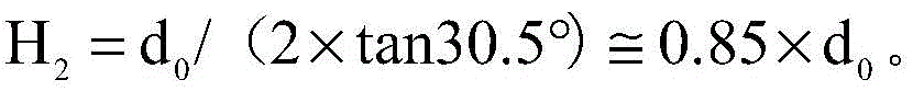
substituting the value of alpha 1 into formula (2) can obtain the first distance H
1Satisfies the following conditions:
substituting the value of
α 2 into equation (4) can yield the second distance H
2Satisfies the following conditions:
that is, the distance h1 between the edge aa of the
first prism 022a close to the
display cover 021 and extending along the first direction X and the
display cover 021 satisfies: h1 is more than or equal to 0.85 xd
0And a distance h2 between an edge bb of the
second prism 022b close to the
display cover 021 and extending along the first direction X and the
display cover 021 satisfies: h2 is more than or equal to 0.85 xd
0。
In the embodiment of the present invention, in order to ensure the display effect of the tiled display panel, the side of the first prism 022a close to the second prism 022b and the side of the second prism 022b close to the first prism 022a may be totally reflected, that is, the incident angle of the light on the side of the first prism 022a close to the second prism 022b and the incident angle on the side of the second prism 022b close to the first prism 022a may be greater than or equal to the first critical angle δ. And because the incident angle of the light at the seam 00a on the side of the first prism 022a close to the second prism 022b is equal to the included angle β 1 between the side of the first prism 022a close to the second prism 022b and the light-emitting surface of the sub display panel. The incident angle of the light at the seam 00a on the side of the second prism 022b close to the first prism 022a is equal to the included angle β 2 between the side of the second prism 022b close to the first prism 022a and the light-emitting surface of the sub display panel. Therefore, with reference to fig. 3-6, to ensure that the light rays at the patchwork 00a (i.e., light rays b1 and b2) are totally reflected at the side of the first prism 022a near the second prism 022b, and at the side of the second prism 022b near the first prism 022 a. An included angle β 1 between the side of the first prism 022a close to the second prism 022b and the light-emitting surface of the sub display panel, and an included angle β 2 between the side of the second prism 022b close to the first prism 022a and the light-emitting surface of the sub display panel may be greater than or equal to the first critical angle δ, that is, β 1 is greater than or equal to δ, and β 2 is greater than or equal to δ.
Thus, the incident angle of the light at the patchwork 00a on the side of the first prism 022a close to the second prism 022b and the incident angle on the side of the second prism 022b close to the first prism 022a are always greater than or equal to the first critical angle δ, so that total reflection can occur on the sides.
It should be noted that the light totally reflected by the side of the first prism 022a close to the second prism 022b and the side of the second prism 022b close to the first prism 022a can be continuously totally reflected by the side of the first prism 022a far from the second prism 022b and the side of the second prism 022b far from the first prism 022a, and will not be refracted to the display cover 021, so that the totally reflected light can be prevented from causing interference to the light entering the optical compensation bar 02 by the sub-display panel.
In the embodiment of the present invention, in order to further ensure that the light beams of the first prism 022a near the side of the second prism 022b and the second prism 022b near the side of the first prism 022a are totally reflected, an included angle β 1 between the side of the first prism 022a near the second prism 022b and the light-emitting surface of the sub display panel, and an included angle β 2 between the side of the second prism 022b near the first prism 022a and the light-emitting surface of the sub display panel may be set to be 2 ° to 5 ° greater than the first critical angle δ.
For example, an included angle β 1 between a side of the first prism 022a close to the second prism 022b and the light-emitting surface of the sub display panel, and an included angle β 2 between a side of the second prism 022b close to the first prism 022a and the light-emitting surface of the sub display panel may be greater than or equal to 42 °. For example, in order to ensure that the light emitted from the seam 00a can be totally reflected by the optical compensation strip 02, the values of the included angle β 1 and the included angle β 2 may be 45 °.
As can be seen from fig. 4 and 6, the side surface of the first prism 022a close to the second prism 022b and the side surface of the second prism 022b close to the first prism 022a may be both flat surfaces, so that the incident angle of the light on the side surface of the first prism 022a close to the second prism 022b may be an included angle β 1 between the side surface of the first prism 022a close to the second prism 022b and the light-emitting surface of the sub display panel, and the incident angle of the light on the side surface of the second prism 022b close to the first prism 022a may be an included angle β 2 between the side surface of the second prism 022b close to the first prism 022a and the light-emitting surface of the sub display panel. The included angle β 1 and the included angle β 2 may be equal to or different from each other, which is not limited in the embodiment of the present invention.
As can be seen with reference to fig. 3 and 5, the at least two prisms 022 may further include: at least one third prism 022c and at least one fourth prism 022 d. That is, the at least two prisms 022 may include one or more third prisms 022c and one or more fourth prisms 022 d. Illustratively, the structure shown in fig. 3 includes two third prisms 022c and two fourth prisms 022 d.
The at least one third prism 022c may be disposed at a side of the first prism 022a away from the second prism 022b, and the at least one fourth prism 022d may be disposed at a side of the second prism 022b away from the first prism 022 a.
The orthographic projection of each third prism 022c on the light emitting surface can be located in the display region 011a of the first sub-display panel 011 in the two adjacent sub-display panels 01, and each third prism 022c can be used for refracting the light emitted from the first sub-display panel 011 to the region corresponding to the seam 00a on the display cover plate 021. The orthographic projection of each fourth prism 022d on the light emitting surface can be located in the display area 012a of the second sub-display panel 012 of the two adjacent sub-display panels 01, and each fourth prism 022d can be used to refract the light emitted by the second sub-display panel 012 to an area corresponding to the seam 00a on the display cover 021.
The third prism 022c and the fourth prism 022d are arranged to ensure that enough light can be refracted from the sub-display panel 01 to the display cover 021, and ensure that the light transmitted from the display cover 021 can effectively eliminate the seam 00 a.
Optionally, the optical compensation strip provided in the embodiment of the present invention may also be without the third prism 022c and the fourth prism 022d, and the light is refracted only by the side of the first prism 022a away from the second prism 022b and the side of the second prism 022b away from the first prism 022a, and the refracted light may be shifted in a direction close to the splice seam 00 a.
As can also be seen from fig. 3 and 5, the side of the third prism 022c away from the first prism 022a and the side of the fourth prism 022d away from the second prism 022b may be a plane or a curved surface, which is not limited in this embodiment of the present invention.
In the embodiment of the present invention, in order to ensure that the light emitted from the sub-display panel 01 can be refracted at the side of the third prism 022c away from the first prism 022a and the side of the fourth prism 022d away from the second prism 022b, it is required to ensure that the incident angle of the light emitted from the first sub-display panel 011 at the side of the third prism 022c away from the first prism 022a and the incident angle of the light emitted from the second sub-display panel 012 at the side of the fourth prism 022d away from the second prism 022b are both smaller than the first critical angle δ. That is, the included angle between the side of the third prism 022c away from the first prism 022a and the light-emitting surface of the sub display panel, and the included angle between the side of the fourth prism 022d away from the second prism 022b and the light-emitting surface of the sub display panel are both smaller than the first critical angle δ.
FIG. 7 is a schematic structural diagram of another optical compensation strip according to an embodiment of the present invention. As can be seen with reference to fig. 7, the plurality of prisms 022 includes: the adjacent first prism 022a and second prism 022 b. The side of the first prism 022a away from the second prism 022b and the side of the second prism 022b away from the first prism 022a are both curved.
Referring to fig. 3, 5 and 7, according to an included angle β 1 between a side surface of the first prism 022a close to the second prism 022b and a light-emitting surface of the sub display panel, it can be determined that a thickness h31 of the first prism 022a may satisfy:
h31=(d0/2). times.tan beta.1 equation (6)
Similarly, according to the included angle β 2 between the side surface of the second prism 022b close to the first prism 022a and the light-emitting surface of the sub-display panel, it can be determined that the thickness h32 of the second prism 0223 can satisfy:
h32=(d0/2). times.tan beta.2 equation (7)
An included angle β 1 between the side of the first prism 022a close to the second prism 022b and the light emitting surface of the sub display panel and an included angle β 2 between the side of the second prism 022b close to the first prism 022a and the light emitting surface of the sub display panel may be equal to each other, and accordingly, the thickness h31 of the first prism 022a and the thickness h32 of the second prism 022b may be equal to each other.
For example, the values of the included angle β 1 and the included angle β 2 are both assumed to be 45 °. The thickness h31 of the first prism 022a can be determined according to equation (4) and equation (5) as: h31 ═ d0/2)=0.5×d0The thickness h32 of the second prism 022b is: h32 ═ d0/2=0.5×d0。
In the embodiment of the present invention, it is assumed that the distance h1 between the edge aa of the first prism 022a close to the display cover 021 and extending along the first direction X and the display cover 021 is equal to the distance h2 between the edge bb of the second prism 022b close to the display cover 021 and extending along the first direction X and the display cover 021. Also, the thickness h31 of the first prism 022a is equal to the thickness h32 of the second prism 022 b. The thickness H of the optical compensation strip 02 satisfies: h is more than H1+ H31.
From the above calculations it can be determined that: h1 is more than or equal to 0.85 xd0,h31=(d0/2)=0.5×d0. Let h1 take on the following values: h1 ═ 0.85 × d0. The thickness H of the optical compensation strip 02 satisfies: h > 1.35 xd0. In consideration of displaying the thickness margin of the cover plate 021, the thickness H of the optical compensation strip 02 may satisfy: h<1.5×d0. Also, in the embodiment of the present invention, the length of the optical compensation strip 02 in the second direction Y may be six times the length of the seam 00a in the second direction Y. Namely, the thickness of the optical compensation strip 02 provided by the embodiment of the invention is relatively thin, so that the problem of relatively heavy weight is avoided.
Fig. 8 is a partially enlarged structural schematic view of the tiled display panel shown in fig. 1. Referring to fig. 8, a first frame length of the frame 011b at the joint of the first sub-display panels 011 of the two adjacent sub-display panels 01 along the second direction may be s1, a second frame length of the frame 012b at the joint of the second sub-display panels 012 of the two adjacent sub-display panels 01 along the second direction may be s2, a sum of the first frame length s1 and the second frame length s2, and a length d of the second groove 023b along the second direction0May be less than the threshold E. That is, the difference between the sum of the lengths (s1+ s2) and the length of the second groove 023b in the second direction may be small, for example, the threshold E may be 0.1mm (millimeters).
In the embodiment of the present invention, the length of the joint 00a between two adjacent sub display panels 01 in the second direction may be equal to the sum of the first frame length s1 of the frame 011b of the first sub display panel 011 in the second direction, the second frame length s2 of the frame 012b of the second sub display panel 012 in the second direction, the length t1 of the non-display region at the joint of the first sub display panel 011 in the second direction, and the length t2 of the non-display region at the joint of the second sub display panel 012 in the second direction. That is, the length d of the patchwork 00a in the second direction0Satisfies the following conditions: d0=s1+s2+t1+t2。
As can be seen by referring to fig. 1, 3, 5 and 7, a length of a side of the prism substrate 023 close to the display cover plate 021 in the second direction Y may be smaller than a length of a side of the prism substrate 023 away from the display cover plate 021 in the second direction Y. The length of the display cover 021 along the second direction Y may be equal to the length of the prism substrate 023 along the second direction Y on a side of the display cover 021.
Alternatively, the cross section of the prism substrate 023 may be a trapezoid structure, a short side of which may be a side adjacent to the display cover plate 021, and a long side of which may be a side adjacent to the sub-display panel. The cross section of the prism substrate 023 is set to be trapezoidal, so that a transition area can exist between the sub-display panel and the display cover plate in the optical compensation strip, and further, the images displayed by the sub-display panel and the images displayed by the display cover plate can be in uniform transition, and the display effect of the spliced display panel is ensured.
Referring to fig. 7, it can also be seen that the waist of the trapezoid structure can be an arc line, and the arc line can be convex toward the groove, so that the structural stability of the optical compensation strip 02 can be improved, and the weight of the optical compensation strip 02 can be reduced. And when the waist of the trapezoidal structure is an arc line, the transition between the image displayed by the display cover plate and the image displayed by the sub-display panel is smoother, and the display effect is better. Of course, the waist of the trapezoid structure may also be a straight line, which is not limited in the embodiment of the present invention.
In the embodiment of the invention, the prism substrate 023 and the display cover plate 021 can be bonded and fixed through optical glue. The optical cement can be OCA (optical clear adhesive) optical cement which has high transmittance and strong adhesive force. And, after laminating through this OCA optical cement, this optical compensation strip 02 can be a whole, be convenient for transportation and installation. Alternatively, the prism substrate 023 and the display cover 021 may be of unitary construction.
Alternatively, the material of the display cover plate 021 may include any one of a copolymer of methyl methacrylate and styrene, polycarbonate, polymethyl methacrylate, or ground glass, or a combination of at least two of the above materials. The material of the prism 022 may include: the composite material is composed of any one of or a combination of at least two of a copolymer of methyl methacrylate and styrene, polycarbonate, polymethyl methacrylate or ground glass. The material of the prism substrate 023 may include: the material is a composition consisting of any one of or at least two of a copolymer of methyl methacrylate and styrene, polycarbonate, polymethyl methacrylate and ground glass. These materials have a transmittance of 90% or more and a refractive index of 1.49 to 1.59, and are similar to the refractive index of the sub-display panel 01, and can be easily processed and extruded.
For example, the display cover 021 may be a rough cover (e.g., may be ground glass), i.e., the surface roughness of the display cover 021 is high. Alternatively, the display 021 can be a gain screen. Thereby, the display effect of the display cover 021 can be improved. The gain screen may be a display screen with high brightness and high transmittance.
Alternatively, in the display cover 021, the prism 022 may be roughened in a region where the orthographic projection of the display cover 021 is located, and a region adjacent to the prism base 023 may not be roughened. Of course, the whole area of the display cover 021 may be roughened, which is not limited in the embodiment of the present invention.
Alternatively, the surface roughness of the area where the prism substrate 023 contacts the sub display panel 01 may be greater than a roughness threshold. That is, the surface roughness of the area where the prism substrate 023 contacts the sub-display panel 01 is higher, so that the area is ensured not to generate image distortion, and the display effect of the tiled display panel is improved.
In the embodiment of the present invention, one end of the optical compensation strip 02 may be a tip, and an angle of the tip is positively correlated with a length of the seam 00a along the second direction.
In manufacturing the optical compensation strip 02, one end of the optical compensation strip 02 may be cut into a tip. FIG. 9 is a top view of an optical compensation strip according to an embodiment of the present invention. FIG. 10 is a schematic diagram of the cutting of an optical compensation strip according to an embodiment of the present invention, and referring to FIG. 10, it can be seen that the angle γ of the cut tip1Can be bluntAnd (4) an angle. FIG. 11 is a schematic diagram of another cut-out of an optical compensation strip according to an embodiment of the present invention, as can be seen with reference to FIG. 11, the angle γ of the cut-out tip2May be acute. FIG. 12 is a schematic diagram of another cutting of an optical compensation strip according to an embodiment of the present invention. Referring to fig. 12, it can be seen that the angle γ of the cut tip may be a right angle. That is, γ1>γ>γ2。
Fig. 13 is a schematic structural diagram of another tiled display panel according to an embodiment of the present invention. As can be seen with reference to fig. 13, the tiled display panel may include four sub display panels 011, 012, 013 and 014, and four optical compensation bars 02a, 02b, 02c and 02 d. The first optical compensation strip 02a is located at a seam between the first sub display panel 011 and the second sub display panel 012, the second optical compensation strip 02b is located at a seam between the third sub display panel 013 and the fourth sub display panel 014, the third optical compensation strip 02c is located at a seam between the first sub display panel 011 and the third sub display panel 013, and the fourth optical compensation strip 02d is located at a seam between the second sub display panel 012 and the fourth sub display panel 014.
Referring to fig. 13, it can be seen that the tiled display panel can be formed by tiling four sub-display panels 01, and there are four seams in the tiled display panel. If the extending direction of the longer side of the tiled display panel is defined as the longitudinal direction V, the extending direction of the shorter side is defined as the width direction U. Then, of the four joints in the tiled display panel, the extending directions of two joints and the optical compensation strips covering the two joints are parallel to the length direction V, and the extending directions of the other two joints and the optical compensation strips covering the two joints are parallel to the width direction U.
For example, referring to fig. 13, the extending direction of the seam between the first sub display panel 011 and the second sub display panel 012 and the first optical compensation strip 02a covering the seam are parallel to the width direction U. The extending direction of the seam between the third sub display panel 013 and the fourth sub display panel 014 and the second optical compensation strip 02b covering the seam are both parallel to the width direction U. That is, for the first and second optical compensation strips 02a and 02b, the first direction X is parallel to the width direction U, and the second direction Y is parallel to the length direction V. The extending direction of the seam between the first sub display panel 011 and the third sub display panel 013 and the third optical compensation bar 02c covering the seam are both parallel to the length direction V. The extending directions of the joint between the second sub-display panel 012 and the fourth sub-display panel 014 and the fourth optical compensation strip 02d covering the joint are both parallel to the length direction V. That is, for the third optical compensation stripe 02c and the fourth optical compensation stripe 02d, the first direction X is parallel to the length direction V, and the second direction Y is parallel to the width direction U.
Referring to fig. 13, it can be seen that the length of the seam between the first sub display panel 011 and the second sub display panel 012 in the length direction V is equal to the length of the seam between the third sub display panel 013 and the fourth sub display panel 014 in the length direction V. The length of the seam between the first sub display panel 011 and the third sub display panel 013 in the length direction V is equal to the length of the seam between the second sub display panel 012 and the fourth sub display panel 014 in the length direction V. Further, the length of the seam between the first sub display panel 011 and the second sub display panel 012 in the length direction V is larger than the length of the seam between the first sub display panel 011 and the third sub display panel 013 in the length direction V.
Therefore, the length of the first optical compensation stripe 02a in the length direction V and the length of the second optical compensation stripe 02b in the length direction V may be equal, the length of the third optical compensation stripe 02c in the length direction V and the length of the fourth optical compensation stripe 02d in the length direction V may be equal, and the length of the first optical compensation stripe 02a in the length direction V is greater than the length of the third optical compensation stripe 02c in the length direction V. Accordingly, the angle of the tip of the first optical compensation strip 02a and the angle of the tip of the second optical compensation strip 02b may be equal, the angle of the tip of the third optical compensation strip 02c and the angle of the tip of the fourth optical compensation strip 02d may be equal, and the angle γ of the tip of the first optical compensation strip 02a1Is larger than the included angle gamma of the tip of the third optical compensation strip 02c2。
For example, the first optical compensation strip 02a and the second optical compensation strip 02b may be cut by the cutting method of the optical compensation strip shown in fig. 10. The third optical compensation strip 02c, and the fourth optical compensation strip 02d, can be cut in the cutting manner shown in fig. 11.
Of course, the lengths of the seams 00a between any two adjacent sub-display panels 01 in the tiled display panel along the second direction may also be equal. Accordingly, the included angle γ of the tip of each optical compensation strip 02 in the tiled display panel can be 90 °, that is, each optical compensation strip 02 can be cut in the manner shown in fig. 12.
Through the length along the second direction according to the piece between the adjacent sub-display panel, cut optical compensation strip 02, can guarantee when including a plurality of optical compensation strips 02 in the concatenation display panel, this adjacent optical compensation strip 02 can be accurate concatenation together, ensures that the piece between the sub-display panel can effectively be eliminated.
It should be noted that the light emitting surfaces described in the embodiments of the present invention refer to light emitting surfaces of sub display panels in a tiled display panel, and the light emitting surfaces of the sub display panels in the tiled display panel may be coplanar.
In summary, the embodiments of the present invention provide an optical compensation strip, which can be applied to a tiled display panel. Each optical compensation strip includes: the display cover plate and at least two prisms arranged opposite to the display cover plate. A gap exists between each prism and the display cover plate. The at least two prisms are used for refracting light rays emitted by the two adjacent sub-display panels to the area, corresponding to the splicing seam, on the display cover plate, so that the area, corresponding to the splicing seam, of the display cover plate can also display images, and the effect of eliminating the splicing seam is achieved. And when assembling the spliced display panel, only the optical compensation strip needs to be attached to the splicing seam between two adjacent sub-display panels, so that the installation is convenient and the cost is low.
An embodiment of the present invention provides a display device, which may include: at least two sub-display panels 01, at least one optical compensation strip 02 provided by the above embodiments, and at least two backlight modules corresponding to the at least two sub-display panels 01 one to one. Each optical compensation strip 02 may be located on the light emitting surfaces of two adjacent sub-display panels 01, and cover the seam between the two adjacent sub-display panels 01. Each backlight module may be located at the light incident surface of the corresponding sub display panel 01. For example, the display device may include an optical compensation strip 02 as shown in any one of fig. 2 to 7.
Optionally, each backlight module in the display device may be a direct type backlight module. The light source in the direct type backlight module is arranged at the bottom of the light guide plate.
Fig. 14 is a flowchart of a driving method of a backlight module according to an embodiment of the invention. The driving method can be used for driving a backlight module in a display device, and the optical compensation strip in the display device can be any one of the optical compensation strips shown in fig. 2 to 7. The backlight module is arranged on the light incident surface of the target sub-display panel and is a direct type backlight module, and a light source of the backlight module can comprise a plurality of light emitting units. Referring to fig. 14, the method may include:
step 101, determining a brightness compensation coefficient according to the first length of the reducing display area in the display area of the target sub-display panel and the sum of the first length of the reducing display area and the second length of the compensation display area.
The brightness compensation coefficient can be larger than 1, and is negatively correlated with the first length and positively correlated with the sum of the lengths. The reducing display area is an area covered by orthographic projection of at least two prisms in the target optical compensation strip in the display area, namely, an area where light rays emitted from the display area are refracted by the target optical compensation strip, and the reducing display area can extend along the first direction. The compensation display area is an area covering the seam in the optical compensation strip, that is, the light incident to the optical compensation strip in the compensation display area can be totally reflected by the target optical compensation strip, and the compensation display area can extend along the first direction. The first length may be a length of the variable diameter display region along the second direction Y, and the second length may be a length of the compensation display region along the second direction. The target optical compensation strip is arranged on the light emergent surface of the target sub-display panel and extends along the first direction. The second direction may be perpendicular to the first direction, and the first direction and the second direction may be both parallel to the light emitting surface.
Alternatively, the brightness compensation factor may be a ratio of the sum of the lengths to the first length.
Fig. 15 is a schematic structural diagram of a target sub-display panel according to an embodiment of the present invention. Referring to fig. 15, it is assumed that the length of the display area of the target sub display panel in the second direction is L0. The display area may be divided into a normal display area and a variable diameter display area. The normal display area may refer to an area of the display area of the target sub-display panel that is not covered by the orthographic projection of the at least two prisms in the target optical compensation bar, that is, an area of the display area of the target sub-display panel where the emitted light is not refracted by the prisms of the area of the optical compensation bar that is covered by the orthographic projection of the at least two prisms in the target optical compensation bar, and referring to fig. 15, the length of the normal display area in the second direction is L2. The variable diameter display area may refer to an area of the display area of the target sub-display panel covered by orthographic projection of at least two prisms in the target optical compensation bar, that is, an area where light emitted from the display area of the target sub-display panel is refracted by the prisms in the optical compensation bar. For example, in the structures shown in fig. 3 and 5, assuming that the target sub-display panel is the first sub-display panel, the variable diameter display area of the first sub-display panel may include: the side face of the first prism, which is far away from the second prism, in the optical compensation strip and the area where the orthographic projection of the third prism on the light-emitting face is located.
Referring to fig. 15, it can be seen that the sum of the length L0 of the display area of the target sub display panel in the second direction and the length of the compensation display area in the second direction is L1. That is, after the patchwork between the target sub-display panel and the adjacent sub-display panel is eliminated by the target optical compensation strip, the length of the area in the second direction where the image can be actually displayed is L1.
For example, referring to fig. 15, it is assumed that the light-emitting surface of the target sub-display panel is provided with two target optical compensation strips, and each target optical compensation strip is arranged on the light-emitting surface of the target sub-display panelThe first directions of the optical compensation strips are all parallel to the width direction U of the target sub-display panel. The display area of the target sub-display panel may include two variable diameter display areas extending along a first direction, and two compensation display areas extending along the first direction are respectively formed at two sides of the display area. Assuming that the lengths of the two variable diameter display areas along the second direction are equal to each other, d2And/2, the total length of the variable diameter display area of the target sub-display panel along the second direction is d2. The lengths of the compensation display areas in the optical compensation strips along the second direction are equal and are d0And/2, the total length of the compensation display area in the optical compensation bar along the second direction is d0. The total length d of the compensation display area0Total length d of display area with variable diameter2Is d1. From the above analysis, it can be determined that the length L1 of the target sub-display panel satisfies: l1 ═ L0+ d0=L2+d1=L2+d0+d2The length L0 of the display area of the target sub-display panel satisfies: l0 ═ L2+ d2。
As can be seen from FIGS. 3, 5 and 7, d0I.e. the length of the seam 00a in the tiled display panel along the second direction.
Suppose that the Total number of pixels of the image displayed in the target sub-display panel is Total. After the seams between the target sub-display panel and the adjacent sub-display panel are eliminated, the area of the target sub-display panel displaying the image is increased, and thus the pixel density of the image displayed in the sub-display panel is changed accordingly.
When the seams in the tiled display panel are not eliminated, the area of the target sub-display panel displaying the image includes: a normal display area and a variable display area (i.e., the display area of the target sub-display panel). At this time, the area of the target sub-display panel actually displaying the image is the display area. The length of the display area is L0, the pixel density p0 of the image displayed by the target sub-display panel may be: p0 Total/L0.
After the seams in the tiled display panel are eliminated by the optical compensation strip provided by the embodiment of the present invention, since the area of the optical compensation strip covering the seams can also display images, the combined area of the target sub-display panel and the target optical compensation strip displaying images includes: the normal display area and the reducing display area of the target sub-display panel, and the compensation display area in the target optical compensation strip. Wherein, the compensation display area in the optical compensation strip is the area of covering the seam in the optical compensation strip. The image displayed in the diameter-reduced display area of the target sub-display panel needs to be displayed after being refracted through the optical compensation strips. At this time, the length of the combined area of the target sub-display panel and the optical compensation bar actually displaying an image in the second direction Y is L1. In order to normally display an image in the combined area with the length of L1, the pixel densities of the image in the variable diameter display area and the normal display area need to be adjusted, so that after the pixel density is adjusted, the pixel density p1 of the image displayed in the combined area is the average of the Total number of pixels Total over the length of L1, that is, the pixel density p1 of the image displayed in the combined area is: p1 Total/L1.
Since the light emitted from the normal display area is not refracted after the patchwork is eliminated by the target optical compensation strip, the pixel density p2 of the image displayed in the normal display area can satisfy the following conditions: p2 (p 1) Total/L1 (p0 × L0)/L1. The first scaling factor k1 for the normal display area may be written as: k1 ═ p0/p 2.
Assuming that the pixel density of the image displayed by the variable diameter display area after the seam is eliminated is p3, the second scaling factor k2 of the variable diameter display area can be recorded as: k2 ═ p0/p 3.
Since the Total number of pixels Total of the image displayed by the target sub-display panel is equal before and after the elimination of the patchwork, it can be deduced that:
L2×p2+d2x p3 Total formula (6)
The following can be solved by equation (6):
p3=[(L1-L2)/(L1×d2)]×Total。
thus, the first scaling factor k1 may be: k1, p0, p2, L1, L0, and the second scaling factor k2 may be: k2 ═ p0/p3 ═ L1 xd (L1 xd)2)/[L0×(L1-L2)]=(L1×d2)/(L0×d1)。
Since the luminance compensation coefficient k may be a ratio of the first scaling coefficient k1 and the second scaling coefficient k 2: k1/k 2d1/d2. Therefore, the sum d of the lengths of the reducing display area and the compensating display area along the second direction can be adjusted1And the length d of the diameter-variable display area along the second direction2Is determined as the luminance compensation coefficient k.
Optionally, the brightness compensation coefficient may also be: k is k1/k2+ epsilon. Wherein E may be a difference between a sum of lengths of the frames of the target sub-display panel and the adjacent sub-display panel along the second direction and a length of the second groove along the second direction, i.e. E < E.
It should be noted that, when the target sub-display panel is a sub-display panel located at an edge of the tiled display panel, the light exit surface of the target sub-display panel may only be provided with one target optical compensation strip extending along the first direction. At this time, the display area of the target display panel may only include a variable diameter display area extending along the first direction, and only one side of the variable diameter display area is formed with a compensation display area extending along the first direction. At this time, the brightness compensation coefficient of the target sub-display panel may be calculated according to the length of the one reducing display area in the second direction and the length of the one compensation display area in the second direction. The calculation process may refer to the above embodiments, and is not described herein again.
And 102, compensating the driving current of the target light-emitting unit in the plurality of light-emitting units according to the brightness compensation coefficient k.
And after the driving current of the target light-emitting unit in the plurality of light-emitting units is compensated according to the brightness compensation coefficient k, the ratio of the driving current of the target light-emitting unit to the driving currents of other light-emitting units is the brightness compensation coefficient. Wherein, the orthographic projection of the target light-emitting unit on the target sub-display panel is positioned in the reducing display area. Because the brightness compensation coefficient is larger than 1, after the brightness compensation coefficient is adopted to compensate the driving current of the target light-emitting unit, the brightness of the target light-emitting unit is larger than the brightness of other light-emitting units, so that the brightness of the reducing display area can be increased, and the brightness compensation of the reducing display area is realized.
Because the light emitted by the diameter-variable display area in the target sub-display panel is refracted to the display cover plate, the area covered by the refracted light in the display cover plate is larger than the diameter-variable display area, so that the brightness of the display cover plate is lower than that of the normal display area in the target sub-display panel under the same backlight brightness. Therefore, the method provided by the embodiment of the invention can ensure that the brightness, the contrast, the chromaticity and the like of all parts of the spliced display panel are kept consistent by compensating the brightness of the reducing display area, and the display effect is better.
In the embodiment of the present invention, if the light emitting surface of the target sub-display panel is provided with an optical compensation strip extending along the width direction U of the tiled display panel and an optical compensation strip extending along the length direction V of the tiled display panel. The width direction U may be taken as the first direction of the optical compensation strip to determine the brightness compensation coefficient by the method shown in the above step 101. And, the determined brightness compensation coefficient can be used to compensate the driving current of the target light-emitting unit in the backlight module. The orthographic projection of the target light-emitting unit on the target sub-display panel is positioned in a reducing display area extending along the width direction U of the target sub-display panel.
Similarly, the length direction V may be used as the first direction of the optical compensation strip to determine the brightness compensation coefficient by the method shown in step 101. And the determined brightness compensation coefficient can be adopted to compensate the driving current of the target light-emitting unit in the backlight module. The orthographic projection of the target light-emitting unit on the target sub-display panel is positioned in a reducing display area extending along the length direction V of the target sub-display panel.
The orthographic projection of the other light-emitting units on the target sub-display panel can be located in a normal display area (i.e. an area where the emitted light is not refracted) of the target sub-display panel.
In an embodiment of the present invention, the light emitting unit may be a Light Emitting Diode (LED).
In summary, embodiments of the present invention provide a driving method of a backlight module, in which a luminance compensation coefficient is determined according to a first length of a variable diameter display region and a sum of the first length of the variable diameter display region and a second length of a compensation display region. And the driving current of the target light-emitting unit corresponding to the reducing display area in the backlight module is adjusted through the brightness compensation coefficient, so that the brightness compensation of the reducing display area is realized, the brightness uniformity of the spliced display panel is improved, and the display effect of the spliced display panel is better.
Fig. 16 is a flowchart of a method for driving a sub-display panel according to an embodiment of the present invention. The driving method may be used to drive a target sub-display panel in the tiled display panel shown in any one of fig. 1, 8, or 13, and the light-emitting surface of the target sub-display panel may be provided with an optical compensation strip extending along the first direction. Referring to fig. 16, the method may include:
step 201, respectively determining a first scaling factor for scaling the normal display area of the target sub-display panel along the second direction, and a second scaling factor for scaling the variable diameter display area of the target sub-display panel along the second direction.
Wherein the first scaling factor k1 is positively correlated with the sum L1 of the lengths of the normal display area, the variable diameter display area and the compensation display area of the target optical compensation strip along the second direction, and is negatively correlated with the sum L0 of the lengths of the normal display area and the variable diameter display area along the second direction, and the second scaling factor k2 is respectively correlated with the sum L1 of the lengths of the normal display area, the variable diameter display area and the compensation display area along the second direction, and the length d of the variable diameter display area along the second direction2Positively correlated with the sum L0 of the lengths of the normal display area and the variable diameter display area along the second direction, and the sum d of the lengths of the variable diameter display area and the compensation display area along the second direction1A negative correlation.
The second direction is perpendicular to the first direction, and the second direction and the first direction may be parallel to the light emitting surface.
The variable diameter display area is an area covered by orthographic projections of at least two prisms in the target optical compensation strip in the display area, namely, an area where light rays emitted in the display area are refracted by the optical compensation strip, the normal display area is an area not covered by orthographic projections of at least two prisms in the target optical compensation strip in the display area, namely, an area where light rays emitted in the display area are not refracted by the optical compensation strip, and the compensation display area is an area covered by a splicing seam in the target optical compensation strip, namely, an area where the splicing seam of the target sub-display panel and an adjacent sub-display panel is located.
Optionally, the first scaling factor k1 may satisfy: k1 — L1/L0, the second scaling factor k2 may satisfy: k2 ═ L1 × d2)/(L0×d1)。
It is assumed that two target optical compensation strips are disposed on the light-emitting surface of the target sub-display panel, and the first direction of each target optical compensation strip is parallel to the width direction U of the target sub-display panel. The display area of the target sub-display panel may include two variable diameter display areas extending along a first direction, and two compensation display areas extending along the first direction are respectively formed at two sides of the display area. Assuming that the lengths of the two variable diameter display regions along the second direction are equal, both the lengths can be d2And/2, the lengths of the compensation display areas on the two sides of the target sub-display panel along the second direction are equal, namely d can be the same0And/2, the total length of the compensation display area of the target sub-display panel along the second direction is d0. The total length d of the compensation display area along the second direction0The total length d of the diameter-variable display area along the second direction2Is d1. From the above analysis, it can be determined that the length L1 in the second direction of the target sub-display panel satisfies: l1 ═ L0+ d0=L2+d1=L2+d0+d2The length L0 of the display area of the target sub-display panel in the second direction satisfies: l0 ═ L2+ d2。
It should be noted that, when the target sub-display panel is a sub-display panel located at an edge of the tiled display panel, the light exit surface of the target sub-display panel may only be provided with a target optical element extending along the first directionAnd (4) compensating bars. At this time, the display area of the target display panel may only include a variable diameter display area extending along the first direction, and only one side of the variable diameter display area is formed with a compensation display area extending along the first direction. At this time, the first scaling factor k1 may be calculated according to a length L1 of the region of the target sub display panel actually displaying the image in the second direction and a length L0 of the display region of the target sub display panel in the second direction, wherein L1 is L0+ d0/2=L2+d1/2=L2+d0/2+d2/2. According to the length L1 of the region of the target sub-display panel actually displaying the image along the second direction, the length L0 of the display region of the target sub-display panel along the second direction, the sum d of the total length of the compensation display region of the target sub-display panel along the second direction and the total length of the reducing display region along the second direction1/2 and the total length d of the variable diameter display area of the target sub-display panel along the second direction2The second scaling factor k2 is calculated by/2. The calculation process may refer to the above embodiments, and is not described herein again.
And step 202, zooming the image in the normal display area of the target sub-display panel along a second direction according to the first zooming coefficient.
In an embodiment of the invention, the driving device may scale the image in the normal display area of the target sub-display panel by the first scaling factor in the second direction. Since the first scaling factor is greater than 1, the ratio of the length of the scaled image along the second direction to the length of the image before scaling along the second direction is the first scaling factor. That is, the driving means performs enlargement processing on the image of the normal display area of the target sub display panel according to the first scaling factor, thereby avoiding image distortion.
Optionally, the first scaling factor k1 may be: and k1 is L1/L0, the driving apparatus may scale the image within the normal display area of the target sub display panel by L1/L0 times in the second direction.
And step 203, zooming the image in the reducing display area of the target sub-display panel along a second direction according to the second zooming coefficient.
In the embodiment of the invention, the driving device may scale the image in the reducing display area of the target sub-display panel by the second scaling factor in the second direction.
Optionally, the second scaling factor k2 may be: k2 ═ L1 × d2)/(L0×d1) The driving means may then scale the image within the reduced diameter display area of the target sub-display panel in a second direction (L1 × d)2)/(L0×d1) And (4) doubling.
It should be noted that, step 202 and step 203 of the driving method for a sub-display panel provided in the embodiment of the present invention may be executed synchronously, or step 203 may also be executed before step 202, which is not limited in the embodiment of the present invention.
In the embodiment of the invention, if the light-emitting surface of the target sub-display panel is provided with the optical compensation strips extending along the length direction V and the optical compensation strips extending along the width direction U. The first scaling factor and the second scaling factor may be determined by the method shown in step 201 above with the width direction U of the target sub-display panel as the first direction. Moreover, the determined first scaling factor may be used to scale the image of the normal display area in the target sub-display panel along the length direction V of the target sub-display panel, and the determined second scaling factor may be used to scale the image of the variable diameter display area in the target sub-display panel along the length direction V of the target sub-display panel.
Similarly, the first scaling factor and the second scaling factor may also be determined by the method shown in step 201 above with the length direction V of the target sub-display panel as the first direction. And the determined first scaling factor can be used for scaling the image of the normal display area in the target sub-display panel along the width direction U of the target sub-display panel, and the determined second scaling factor is used for scaling the image of the variable diameter display area in the target sub-display panel along the width direction U of the target sub-display panel.
Assume that a tiled display panel includes M rows and N columns of sub-display panels (i.e., includes M × N sub-displays tiled with each otherPanel), the second direction is a length direction V of the target sub-display panel and is a row direction of the tiled display panel, and a first scaling factor k1 and a second scaling factor k2 of each sub-display panel along the second direction are equal. The first overall scaling factor k1 of the image displayed by the tiled display panel in the second directionNCan be as follows: k1NK1 xn (L1/L0) xn, the second overall scaling factor k2 in the second directionNCan be as follows: k2N=k2×N=[(L1/d2)/(L0×d1)]And (4) times N. If the second direction is the width direction U of the target sub-display panel and is the row direction of the tiled display panel, and the first scaling factor k1 and the second scaling factor k2 of each sub-display panel along the second direction are all equal. The first total scaling factor k1 of the image displayed by the tiled display panel along the second directionMCan be as follows: k1MK1 × M (L1/L0) × M, a second overall scaling factor k2 in the second directionMCan be as follows: k2M=k2×M=[(L1/d2)/(L0×d1)]×M。
In summary, the present invention provides a driving method of a sub-display panel, which can respectively determine a first scaling factor of a normal display area of a target sub-display panel along a second direction and a second scaling factor of a variable diameter display area of the target sub-display panel along the second direction. And the normal display area in the target sub-display panel is zoomed through the first zoom coefficient, and the variable diameter display area in the target sub-display panel is zoomed through the second zoom coefficient, so that the image displayed in the target sub-display panel is prevented from being distorted, and the image display effect of the splicing display panel is improved.
The embodiment of the invention also provides a driving device of the backlight module, and the driving device can be used for driving the backlight module in the display device. The backlight module is arranged on the light incident surface of the target sub-display panel and is a direct type backlight module, and a light source of the backlight module can comprise a plurality of light emitting units. As shown in fig. 17, the apparatus may include:
the determining module 1701 is configured to determine a brightness compensation coefficient according to the first length of the variable diameter display area and the sum of the first length of the variable diameter display area and the second length of the compensation display area in the display area of the target sub-display panel.
The brightness compensation coefficient can be greater than 1, and the brightness compensation coefficient can be negatively correlated with the first length and positively correlated with the sum of the lengths.
The compensation module 1702 is configured to compensate a driving current of a target light emitting unit of the plurality of light emitting units according to the luminance compensation coefficient.
Wherein, the orthographic projection of the target light-emitting unit on the target sub-display panel can be positioned in the reducing display area. The variable diameter display area may be an area covered by orthographic projections of at least two prisms in the target optical compensation strip in the display area, the compensation display area may be an area covered by a patchwork in the target optical compensation strip, the first length may be a length of the variable diameter display area along a second direction, the second length may be a length of the compensation display area along the second direction, the target optical compensation strip may be disposed on a light-emitting surface of the target sub-display panel and extends along the first direction, the second direction may be perpendicular to the first direction, and the first direction and the second direction may both be parallel to the light-emitting surface.
Optionally, the determining module 1701 is configured to determine a ratio of the sum of the lengths to the first length as the brightness compensation coefficient.
Optionally, the compensation module 1702 is configured to adjust a driving current of the target light emitting unit, so that a ratio of the adjusted driving current of the target light emitting unit to the driving currents of the other light emitting units is a luminance compensation coefficient.
In summary, the driving apparatus for a backlight module provided in the embodiments of the present invention can determine a brightness compensation coefficient according to the determining module, and the compensating module can adjust the driving current of the target light-emitting unit corresponding to the variable diameter display area in the backlight module according to the brightness compensation coefficient, so as to implement brightness compensation for the variable diameter display area, improve the brightness uniformity of the tiled display panel, and achieve a better display effect of the tiled display panel.
The embodiment of the invention also provides a driving device of the sub-display panel, the driving device can be used for driving the target sub-display panel in the spliced display panel, and the light emergent surface of the target sub-display panel can be provided with the target optical compensation strip extending along the first direction. As shown in fig. 18, the apparatus may include:
the determining module 1801 is configured to determine a first scaling factor by which the normal display area of the target sub-display panel is scaled along the second direction, and a second scaling factor by which the variable diameter display area of the target sub-display panel is scaled along the second direction.
The first zoom factor may be positively correlated with a sum of lengths of the normal display area, the variable diameter display area, and the compensation display area of the target optical compensation strip along the second direction, and may be negatively correlated with a sum of lengths of the normal display area and the variable diameter display area along the second direction, and the second zoom factor may be positively correlated with a sum of lengths of the normal display area, the variable diameter display area, and the compensation display area along the second direction, and may be negatively correlated with a sum of lengths of the normal display area and the variable diameter display area along the second direction, and a sum of lengths of the variable diameter display area and the compensation display area along the second direction, respectively.
The second direction may be perpendicular to the first direction, and both the first direction and the second direction are parallel to the light emitting surface.
And a first scaling module 1802, configured to scale the image in the normal display area of the target sub-display panel along the second direction according to the first scaling factor.
The second scaling module 1803 is configured to scale, according to the second scaling factor, an image in the variable diameter display area of the target sub-display panel along the second direction.
The variable diameter display area is an area covered by orthographic projections of at least two prisms in the target optical compensation strip in the display area, the normal display area is an area not covered by orthographic projections of at least two prisms in the target optical compensation strip in the display area, and the compensation display area is an area covered by a splicing seam in the target optical compensation strip.
Optionally, the first scaling factor k1 may satisfy: k1 ═ L1/L0;
the second scaling factor k2 may satisfy: k2 ═ L1 × d2)/(L0×d1);
Wherein L1 is the sum of the lengths of the normal display area, the variable diameter display area and the compensation display area along the second direction, L0 is the sum of the lengths of the normal display area and the variable diameter display area along the second direction, d2The length of the display area with variable diameter along the second direction, d1The sum of the lengths of the reducing display area and the compensation display area along the second direction.
In summary, the driving apparatus for sub-display panels provided in the embodiments of the present invention may determine the first scaling factor and the second scaling factor according to the determining module, where the first scaling module scales the image in the normal display area of the target sub-display panel according to the first scaling factor, and the second scaling module scales the image in the variable diameter display area of the target sub-display panel according to the second scaling factor, so as to avoid distortion of the image displayed in the target sub-display panel, and improve stability of the image displayed by the tiled display panel.
It can be clearly understood by those skilled in the art that, for convenience and brevity of description, the specific working processes of the above-described apparatuses and modules may refer to the corresponding processes in the foregoing method embodiments, and are not described herein again.
The embodiment of the present invention further provides another driving apparatus, which may include: the processing component can be a processing circuit or a processing unit, and the processing component can implement the driving method of the backlight module or the driving method of the sub-display panel provided by the above method embodiment when executing the computer program.
In the embodiment of the present invention, the driving device may be a control chip independently integrated in the display device, or may be integrated on a System On Chip (SOC) or a display card of the display device.
The embodiment of the present invention further provides a computer-readable storage medium, where instructions are stored in the computer-readable storage medium, and when the computer-readable storage medium runs on a computer, the computer is enabled to execute the driving method of the backlight module or the driving method of the sub display panel provided in the above method embodiment.
The above description is only exemplary of the present application and should not be taken as limiting, as any modification, equivalent replacement, or improvement made within the spirit and principle of the present application should be included in the protection scope of the present application.