CN109427847B - Manufacturing method of light-emitting layer, electroluminescent device and display device - Google Patents
Manufacturing method of light-emitting layer, electroluminescent device and display device Download PDFInfo
- Publication number
- CN109427847B CN109427847B CN201710758714.2A CN201710758714A CN109427847B CN 109427847 B CN109427847 B CN 109427847B CN 201710758714 A CN201710758714 A CN 201710758714A CN 109427847 B CN109427847 B CN 109427847B
- Authority
- CN
- China
- Prior art keywords
- solution
- pixel
- retaining wall
- layer
- light
- Prior art date
- Legal status (The legal status is an assumption and is not a legal conclusion. Google has not performed a legal analysis and makes no representation as to the accuracy of the status listed.)
- Active
Links
Images


Classifications
-
- H—ELECTRICITY
- H10—SEMICONDUCTOR DEVICES; ELECTRIC SOLID-STATE DEVICES NOT OTHERWISE PROVIDED FOR
- H10K—ORGANIC ELECTRIC SOLID-STATE DEVICES
- H10K59/00—Integrated devices, or assemblies of multiple devices, comprising at least one organic light-emitting element covered by group H10K50/00
- H10K59/10—OLED displays
- H10K59/12—Active-matrix OLED [AMOLED] displays
- H10K59/122—Pixel-defining structures or layers, e.g. banks
-
- H—ELECTRICITY
- H10—SEMICONDUCTOR DEVICES; ELECTRIC SOLID-STATE DEVICES NOT OTHERWISE PROVIDED FOR
- H10K—ORGANIC ELECTRIC SOLID-STATE DEVICES
- H10K50/00—Organic light-emitting devices
- H10K50/10—OLEDs or polymer light-emitting diodes [PLED]
- H10K50/11—OLEDs or polymer light-emitting diodes [PLED] characterised by the electroluminescent [EL] layers
-
- H—ELECTRICITY
- H10—SEMICONDUCTOR DEVICES; ELECTRIC SOLID-STATE DEVICES NOT OTHERWISE PROVIDED FOR
- H10K—ORGANIC ELECTRIC SOLID-STATE DEVICES
- H10K59/00—Integrated devices, or assemblies of multiple devices, comprising at least one organic light-emitting element covered by group H10K50/00
- H10K59/10—OLED displays
- H10K59/12—Active-matrix OLED [AMOLED] displays
- H10K59/121—Active-matrix OLED [AMOLED] displays characterised by the geometry or disposition of pixel elements
-
- H—ELECTRICITY
- H10—SEMICONDUCTOR DEVICES; ELECTRIC SOLID-STATE DEVICES NOT OTHERWISE PROVIDED FOR
- H10K—ORGANIC ELECTRIC SOLID-STATE DEVICES
- H10K71/00—Manufacture or treatment specially adapted for the organic devices covered by this subclass
-
- H—ELECTRICITY
- H10—SEMICONDUCTOR DEVICES; ELECTRIC SOLID-STATE DEVICES NOT OTHERWISE PROVIDED FOR
- H10K—ORGANIC ELECTRIC SOLID-STATE DEVICES
- H10K71/00—Manufacture or treatment specially adapted for the organic devices covered by this subclass
- H10K71/10—Deposition of organic active material
- H10K71/12—Deposition of organic active material using liquid deposition, e.g. spin coating
- H10K71/13—Deposition of organic active material using liquid deposition, e.g. spin coating using printing techniques, e.g. ink-jet printing or screen printing
- H10K71/135—Deposition of organic active material using liquid deposition, e.g. spin coating using printing techniques, e.g. ink-jet printing or screen printing using ink-jet printing
-
- H—ELECTRICITY
- H10—SEMICONDUCTOR DEVICES; ELECTRIC SOLID-STATE DEVICES NOT OTHERWISE PROVIDED FOR
- H10K—ORGANIC ELECTRIC SOLID-STATE DEVICES
- H10K77/00—Constructional details of devices covered by this subclass and not covered by groups H10K10/80, H10K30/80, H10K50/80 or H10K59/80
-
- H—ELECTRICITY
- H10—SEMICONDUCTOR DEVICES; ELECTRIC SOLID-STATE DEVICES NOT OTHERWISE PROVIDED FOR
- H10K—ORGANIC ELECTRIC SOLID-STATE DEVICES
- H10K77/00—Constructional details of devices covered by this subclass and not covered by groups H10K10/80, H10K30/80, H10K50/80 or H10K59/80
- H10K77/10—Substrates, e.g. flexible substrates
-
- Y—GENERAL TAGGING OF NEW TECHNOLOGICAL DEVELOPMENTS; GENERAL TAGGING OF CROSS-SECTIONAL TECHNOLOGIES SPANNING OVER SEVERAL SECTIONS OF THE IPC; TECHNICAL SUBJECTS COVERED BY FORMER USPC CROSS-REFERENCE ART COLLECTIONS [XRACs] AND DIGESTS
- Y02—TECHNOLOGIES OR APPLICATIONS FOR MITIGATION OR ADAPTATION AGAINST CLIMATE CHANGE
- Y02E—REDUCTION OF GREENHOUSE GAS [GHG] EMISSIONS, RELATED TO ENERGY GENERATION, TRANSMISSION OR DISTRIBUTION
- Y02E10/00—Energy generation through renewable energy sources
- Y02E10/50—Photovoltaic [PV] energy
- Y02E10/549—Organic PV cells
-
- Y—GENERAL TAGGING OF NEW TECHNOLOGICAL DEVELOPMENTS; GENERAL TAGGING OF CROSS-SECTIONAL TECHNOLOGIES SPANNING OVER SEVERAL SECTIONS OF THE IPC; TECHNICAL SUBJECTS COVERED BY FORMER USPC CROSS-REFERENCE ART COLLECTIONS [XRACs] AND DIGESTS
- Y02—TECHNOLOGIES OR APPLICATIONS FOR MITIGATION OR ADAPTATION AGAINST CLIMATE CHANGE
- Y02P—CLIMATE CHANGE MITIGATION TECHNOLOGIES IN THE PRODUCTION OR PROCESSING OF GOODS
- Y02P70/00—Climate change mitigation technologies in the production process for final industrial or consumer products
- Y02P70/50—Manufacturing or production processes characterised by the final manufactured product
Landscapes
- Engineering & Computer Science (AREA)
- Manufacturing & Machinery (AREA)
- Microelectronics & Electronic Packaging (AREA)
- Physics & Mathematics (AREA)
- Geometry (AREA)
- Optics & Photonics (AREA)
- Electroluminescent Light Sources (AREA)
- Devices For Indicating Variable Information By Combining Individual Elements (AREA)
- Application Of Or Painting With Fluid Materials (AREA)
Abstract
本发明公开一种发光层的制造方法、电致发光器件及显示装置,属于显示技术领域。该方法包括:提供形成有像素界定层的衬底基板,像素界定层的多个挡墙结构在衬底基板上限定出多个像素区,多个像素区包括沿第一方向排布的像素区和沿第二方向排布的像素区;通过溶液制程在形成有像素界定层的衬底基板上形成溶液层,溶液层包括形成在多个像素区内的溶液和形成在第一挡墙结构上的溶液,像素区内的溶液与第一挡墙结构上的溶液不融合;对溶液层进行干燥处理,使每个像素区内的溶液形成发光结构,得到发光层。本发明解决了发光层的均一性较差的问题,提高了发光层的均一性。本发明用于电致发光器件。
The invention discloses a method for manufacturing a light-emitting layer, an electroluminescent device and a display device, which belong to the technical field of display. The method includes: providing a base substrate on which a pixel definition layer is formed, a plurality of retaining wall structures of the pixel definition layer define a plurality of pixel regions on the base substrate, and the plurality of pixel regions include pixel regions arranged along a first direction and a pixel area arranged along the second direction; a solution layer is formed on the base substrate formed with the pixel defining layer through a solution process, and the solution layer includes the solution formed in the plurality of pixel areas and formed on the first retaining wall structure The solution in the pixel area is not fused with the solution on the first retaining wall structure; the solution layer is dried to make the solution in each pixel area form a light-emitting structure to obtain a light-emitting layer. The invention solves the problem of poor uniformity of the light-emitting layer and improves the uniformity of the light-emitting layer. The present invention is used in electroluminescent devices.
Description
技术领域technical field
本发明涉及显示技术领域,特别涉及一种发光层的制造方法、电致发光器件及显示装置。The present invention relates to the field of display technology, and in particular, to a method for manufacturing a light-emitting layer, an electroluminescent device and a display device.
背景技术Background technique
有机发光二极管(英文:Organic Light-Emitting Diode;简称:OLED)显示装置具有轻薄、低功耗、高对比度、高色域以及可柔性显示等优点,广泛应用于显示行业。OLED显示装置主要依靠电致发光器件实现图像显示。Organic Light-Emitting Diode (English: Organic Light-Emitting Diode; OLED for short) display devices have the advantages of thinness, low power consumption, high contrast ratio, high color gamut and flexible display, and are widely used in the display industry. OLED display devices mainly rely on electroluminescent devices to realize image display.
电致发光器件通常包括衬底基板以及依次设置在衬底基板上的薄膜晶体管(英文:Thin Film Transistor;简称:TFT)层、阳极层、像素界定层(英文:Pixel DefinitionLayer;简称:PDL)、发光层和阴极层,TFT层包括多个TFT,阳极层包括多个阳极结构,发光层包括多个发光结构,TFT、阳极结构和发光结构三者一一对应,其中,像素界定层包括多个挡墙结构,多个挡墙结构限定出阵列排布的多个像素区,多个像素区包括沿第一方向排布的像素区和沿第二方向排布的像素区,且沿第一方向排布的像素区中任意相邻的两个像素区之间的距离与沿第二方向排布的像素区中任意相邻的两个像素区之间的距离不相等,每个像素区内设置有一个发光结构。目前,通常采用湿法成膜工艺形成发光层,在湿法成膜工艺中,通常先通过溶液制程在像素区内充填溶液,然后采用减压干燥工艺去除像素区内的溶剂,使像素区内的溶质形成发光结构,从而形成发光层。An electroluminescent device usually includes a base substrate and a thin film transistor (English: Thin Film Transistor; abbreviation: TFT) layer, an anode layer, a pixel definition layer (English: Pixel Definition Layer; abbreviation: PDL), which are sequentially arranged on the base substrate. The light-emitting layer and the cathode layer, the TFT layer includes a plurality of TFTs, the anode layer includes a plurality of anode structures, the light-emitting layer includes a plurality of light-emitting structures, and the TFTs, the anode structures and the light-emitting structures are in one-to-one correspondence, wherein the pixel defining layer includes a plurality of A retaining wall structure, the plurality of retaining wall structures define a plurality of pixel regions arranged in an array, and the plurality of pixel regions include pixel regions arranged in a first direction and pixel regions arranged in a second direction, and along the first direction The distance between any adjacent two pixel areas in the arranged pixel areas is not equal to the distance between any adjacent two pixel areas in the pixel areas arranged along the second direction, and each pixel area is set There is a light-emitting structure. At present, the light-emitting layer is usually formed by a wet film forming process. In the wet film forming process, a solution is usually filled in the pixel area through a solution process, and then the solvent in the pixel area is removed by a decompression drying process, so that the pixel area is The solute forms a light-emitting structure, thereby forming a light-emitting layer.
但是,由于沿第一方向排布的像素区中任意相邻的两个像素区之间的距离与沿第二方向排布的像素区中任意相邻的两个像素区之间的距离不相等,在对像素区内的溶液干燥的过程中,像素区中的溶液在第一方向上受到的微作用力与在第二方向上受到的微作用力不同,使溶质在第一方向上的分布与在第二方向上的分布不同;另一方面,由于大部分的像素区为类长方形结构,形成的发光结构也为类长方形结构,使得发光结构的厚度均一性在长轴方向(与发光结构的长边平行的方向)和短轴方向(与发光结构的短边平行的方向)难以同时达到最佳状态,发光结构的形貌较差,导致发光层的均一性较差。However, since the distance between any two adjacent pixel areas in the pixel areas arranged along the first direction is not equal to the distance between any adjacent two pixel areas in the pixel areas arranged along the second direction , in the process of drying the solution in the pixel area, the micro-action force received by the solution in the pixel area in the first direction is different from the micro-action force in the second direction, so that the distribution of the solute in the first direction It is different from the distribution in the second direction; on the other hand, since most of the pixel regions are of a quasi-rectangular structure, the formed light-emitting structure is also a quasi-rectangular structure, so that the thickness uniformity of the light-emitting structure is in the direction of the long axis (the same as that of the light-emitting structure). It is difficult to achieve the optimal state at the same time, and the morphology of the light-emitting structure is poor, resulting in poor uniformity of the light-emitting layer.
发明内容SUMMARY OF THE INVENTION
为了解决发光层的均一性较差的问题,本发明提供一种发光层的制造方法、电致发光器件及显示装置。所述技术方案如下:In order to solve the problem of poor uniformity of the light-emitting layer, the present invention provides a manufacturing method of the light-emitting layer, an electroluminescent device and a display device. The technical solution is as follows:
第一方面,提供一种发光层的制造方法,所述方法包括:In a first aspect, a method for manufacturing a light-emitting layer is provided, the method comprising:
提供形成有像素界定层的衬底基板,所述像素界定层包括多个挡墙结构,所述多个挡墙结构在所述衬底基板上限定出阵列排布的多个像素区,所述多个像素区包括沿第一方向排布的多个像素区和沿第二方向排布的多个像素区,任意相邻的两个沿所述第一方向排布的像素区之间的距离大于任意相邻的两个沿所述第二方向排布的像素区之间的距离;A base substrate formed with a pixel definition layer is provided, the pixel definition layer includes a plurality of retaining wall structures, the plurality of retaining wall structures define a plurality of pixel regions arranged in an array on the base substrate, the The multiple pixel areas include multiple pixel areas arranged along the first direction and multiple pixel areas arranged along the second direction, and the distance between any two adjacent pixel areas arranged along the first direction greater than the distance between any two adjacent pixel regions arranged along the second direction;
通过溶液制程在形成有所述像素界定层的衬底基板上形成溶液层,所述溶液层包括形成在所述多个像素区内的溶液和形成在第一挡墙结构上的溶液,所述第一挡墙结构为所述多个挡墙结构中沿所述第一方向排布的像素区之间的挡墙结构,所述多个像素区中的任一像素区内的溶液与限定所述任一像素区的第一挡墙结构上的溶液不融合;A solution layer is formed on the base substrate on which the pixel defining layer is formed by a solution process, the solution layer includes a solution formed in the plurality of pixel regions and a solution formed on the first retaining wall structure, the The first retaining wall structure is a retaining wall structure between the pixel regions arranged along the first direction among the plurality of retaining wall structures, and the solution in any pixel region of the plurality of pixel regions is connected to the defined limit. The solution on the first retaining wall structure in any of the pixel regions is not fused;
对所述溶液层进行干燥处理,使所述多个像素区中的每个像素区内的溶液形成发光结构,得到发光层。The solution layer is dried, so that the solution in each pixel region of the plurality of pixel regions forms a light-emitting structure to obtain a light-emitting layer.
可选地,所述溶液层还包括形成在第二挡墙结构上的溶液,所述第二挡墙结构为所述多个挡墙结构中沿所述第二方向排布的像素区之间的挡墙结构,所述多个像素区中的任一像素区内的溶液与限定所述任一像素区的第二挡墙结构上的溶液不融合,所述第二挡墙结构上的溶液的溶液量小于所述第一挡墙结构上的溶液的溶液量。Optionally, the solution layer further includes a solution formed on a second retaining wall structure, where the second retaining wall structure is between pixel regions arranged along the second direction in the plurality of retaining wall structures The retaining wall structure, the solution in any pixel region of the plurality of pixel regions is not fused with the solution on the second retaining wall structure that defines any pixel region, and the solution on the second retaining wall structure The amount of the solution is less than that of the solution on the first retaining wall structure.
可选地,所述第一挡墙结构上形成有第一凹槽,所述第一挡墙结构上的溶液位于所述第一凹槽内,在所述通过溶液制程在形成有所述像素界定层的衬底基板上形成溶液层之前,所述方法还包括:通过一次构图工艺对所述像素界定层进行处理,使所述第一挡墙结构上形成第一凹槽。Optionally, a first groove is formed on the first retaining wall structure, the solution on the first retaining wall structure is located in the first groove, and the pixel is formed in the solution process through the solution process. Before forming the solution layer on the base substrate of the defining layer, the method further includes: processing the pixel defining layer through a patterning process to form a first groove on the first retaining wall structure.
可选地,所述第一凹槽的开口面的形状为圆形或方形。Optionally, the shape of the opening surface of the first groove is circular or square.
可选地,沿所述第二方向排布的多个像素区中,位于任意相邻的两个像素区同一侧的两个第一挡墙结构上的第一凹槽连通。Optionally, among the plurality of pixel regions arranged along the second direction, the first grooves on the two first retaining wall structures located on the same side of any two adjacent pixel regions are connected.
可选地,沿所述第二方向排布的多个像素区中,位于任意相邻的两个像素区同一侧的两个第一挡墙结构上的第一凹槽之间形成有第二凹槽,位于所述任意相邻的两个像素区同一侧的两个第一挡墙结构上的第一凹槽通过所述第二凹槽连通,所述通过一次构图工艺对所述像素界定层进行处理,使所述第一挡墙结构上形成第一凹槽,包括:通过一次构图工艺对所述像素界定层进行处理,使所述第一挡墙结构上形成第一凹槽,沿所述第二方向排布的多个像素区中,位于任意相邻的两个像素区同一侧的两个第一挡墙结构上的第一凹槽之间形成第二凹槽,位于所述任意相邻的两个像素区同一侧的两个第一挡墙结构上的第一凹槽通过所述第二凹槽连通。Optionally, among the plurality of pixel regions arranged along the second direction, a second groove is formed between the first grooves on the two first retaining wall structures located on the same side of any adjacent two pixel regions. grooves, the first grooves on the two first retaining wall structures located on the same side of any adjacent two pixel regions are communicated through the second grooves, and the pixels are defined by one patterning process layer processing to form a first groove on the first retaining wall structure, comprising: processing the pixel defining layer through a patterning process to form a first groove on the first retaining wall structure, along the In the plurality of pixel areas arranged in the second direction, a second groove is formed between the first grooves on the two first retaining wall structures on the same side of any adjacent two pixel areas, and is located in the The first grooves on the two first blocking wall structures on the same side of any adjacent two pixel regions are communicated through the second grooves.
可选地,所述第一凹槽的深度大于或等于所述第二凹槽的深度,所述第一凹槽的开口面的面积大于所述第二凹槽的开口面的面积。Optionally, the depth of the first groove is greater than or equal to the depth of the second groove, and the area of the opening surface of the first groove is greater than the area of the opening surface of the second groove.
可选地,所述像素区、所述第一凹槽和所述第二凹槽通过同一次构图工艺形成。Optionally, the pixel region, the first groove and the second groove are formed through the same patterning process.
可选地,所述通过溶液制程在形成有所述像素界定层的衬底基板上形成溶液层,所述溶液层包括形成在所述多个像素区内的溶液和形成在第一挡墙结构上的溶液,包括:Optionally, a solution layer is formed on the base substrate on which the pixel defining layer is formed by a solution process, and the solution layer includes a solution formed in the plurality of pixel regions and a first retaining wall structure on the solution, including:
通过第一溶液制程在所述多个像素区内形成溶液;forming a solution in the plurality of pixel regions by a first solution process;
通过第二溶液制程在所述第一挡墙结构上形成溶液,得到所述溶液层。A solution is formed on the first retaining wall structure through a second solution process to obtain the solution layer.
可选地,所述第一溶液制程包括喷墨打印制程,所述第二溶液制程包括喷墨打印制程和喷涂制程中的任意一种。Optionally, the first solution process includes an inkjet printing process, and the second solution process includes any one of an inkjet printing process and a spray coating process.
可选地,任一所述第一挡墙结构上的溶液的溶液量的取值范围包括:1皮升~200皮升。Optionally, the value range of the solution amount of the solution on any of the first retaining wall structures includes: 1 picoliter to 200 picoliters.
可选地,任一所述第一挡墙结构上的溶液的溶液量的取值范围为10皮升~100皮升。Optionally, the solution amount of the solution on any of the first retaining wall structures ranges from 10 picoliters to 100 picoliters.
第二方面,提供一种电致发光器件,所述电致发光器件包括:采用第一方面或第一方面的任一可选方式所述的方法制造的发光层。In a second aspect, an electroluminescent device is provided, the electroluminescent device comprising: a light-emitting layer manufactured by the method described in the first aspect or any optional manner of the first aspect.
第三方面,提供一种显示装置,所述显示装置包括第二方面所述的电致发光器件。In a third aspect, a display device is provided, and the display device includes the electroluminescent device described in the second aspect.
本发明提供的技术方案带来的有益效果是:The beneficial effects brought by the technical scheme provided by the invention are:
本发明提供的发光层的制造方法、电致发光器件及显示装置,由于第一挡墙结构上设置有溶液,该溶液可以保证在对溶液层进行干燥处理的过程中,像素区中的溶液在第一方向上受到的微作用力与在第二方向上受到的微作用力相同,使溶质在第一方向上的分布与在第二方向上的分布趋于相同,避免由于溶质分布不均匀导致发光结构的厚度的均一性较差,解决了发光层的均一性较差的问题,有助于提高发光层的均一性。In the method for manufacturing a light-emitting layer, an electroluminescent device and a display device provided by the present invention, since the first retaining wall structure is provided with a solution, the solution can ensure that the solution in the pixel area is in the process of drying the solution layer. The micro-action force in the first direction is the same as the micro-action force in the second direction, so that the distribution of the solute in the first direction and the distribution in the second direction tend to be the same, avoiding the uneven distribution of the solute. The uniformity of the thickness of the light-emitting structure is poor, which solves the problem of poor uniformity of the light-emitting layer and helps to improve the uniformity of the light-emitting layer.
应当理解的是,以上的一般描述和后文的细节描述仅是示例性的,并不能限制本发明。It is to be understood that the foregoing general description and the following detailed description are exemplary only and do not limit the invention.
附图说明Description of drawings
为了更清楚地说明本发明实施例中的技术方案,下面将对实施例描述中所需要使用的附图作简单地介绍,显而易见地,下面描述中的附图仅仅是本发明的一些实施例,对于本领域普通技术人员来讲,在不付出创造性劳动的前提下,还可以根据这些附图获得其他的附图。In order to illustrate the technical solutions in the embodiments of the present invention more clearly, the following briefly introduces the accompanying drawings used in the description of the embodiments. Obviously, the accompanying drawings in the following description are only some embodiments of the present invention. For those of ordinary skill in the art, other drawings can also be obtained from these drawings without creative effort.
图1是相关技术提供的发光结构的理论尺寸与实际尺寸的曲线对比图;Fig. 1 is the curve comparison diagram of the theoretical size and the actual size of the light-emitting structure provided by the related art;
图2是本发明实施例提供的一种发光层的制造方法的方法流程图;2 is a method flowchart of a method for manufacturing a light-emitting layer provided by an embodiment of the present invention;
图3是本发明实施例提供的一种形成有像素界定层的衬底基板的示意图;3 is a schematic diagram of a base substrate provided with a pixel defining layer provided in an embodiment of the present invention;
图4是本发明实施例提供的一种在形成有像素界定层的衬底基板上形成溶液层后的示意图;FIG. 4 is a schematic diagram after forming a solution layer on a base substrate with a pixel definition layer formed according to an embodiment of the present invention;
图5是本发明实施例提供的另一种发光层的制造方法的方法流程图;5 is a method flowchart of another method for manufacturing a light-emitting layer provided by an embodiment of the present invention;
图6是本发明实施例提供的另一种在形成有像素界定层的衬底基板上形成溶液层后的示意图;FIG. 6 is another schematic diagram after forming a solution layer on a base substrate on which a pixel defining layer is formed according to an embodiment of the present invention;
图7是本发明实施例提供的再一种发光层的制造方法的方法流程图;FIG. 7 is a method flow chart of still another method for manufacturing a light-emitting layer provided by an embodiment of the present invention;
图8是本发明实施例提供的一种在第一挡墙结构上形成第一凹槽后的示意图;8 is a schematic diagram of a first groove formed on the first retaining wall structure according to an embodiment of the present invention;
图9是本发明实施例提供的另一种在第一挡墙结构上形成第一凹槽后的示意图;9 is another schematic diagram after forming a first groove on the first retaining wall structure according to an embodiment of the present invention;
图10是本发明实施例提供的一种在第一挡墙结构上形成溶液的示意图;10 is a schematic diagram of forming a solution on the first retaining wall structure according to an embodiment of the present invention;
图11是本发明实施例提供的又一种发光层的制造方法的方法流程图;11 is a method flowchart of another method for manufacturing a light-emitting layer provided by an embodiment of the present invention;
图12是本发明实施例提供的一种第一凹槽通过第二凹槽连通的示意图。FIG. 12 is a schematic diagram of a first groove communicating through a second groove according to an embodiment of the present invention.
此处的附图被并入说明书中并构成本说明书的一部分,示出了符合本发明的实施例,并与说明书一起用于解释本发明的原理。The accompanying drawings, which are incorporated in and constitute a part of this specification, illustrate embodiments consistent with the invention and together with the description serve to explain the principles of the invention.
具体实施方式Detailed ways
为了使本发明的目的、技术方案和优点更加清楚,下面将结合附图对本发明作进一步地详细描述,显然,所描述的实施例仅仅是本发明一部分实施例,而不是全部的实施例。基于本发明中的实施例,本领域普通技术人员在没有做出创造性劳动前提下所获得的所有其它实施例,都属于本发明保护的范围。In order to make the objectives, technical solutions and advantages of the present invention clearer, the present invention will be further described in detail below with reference to the accompanying drawings. Obviously, the described embodiments are only a part of the embodiments of the present invention, not all of the embodiments. Based on the embodiments of the present invention, all other embodiments obtained by those of ordinary skill in the art without creative efforts shall fall within the protection scope of the present invention.
电致发光器件通常包括衬底基板以及依次设置在衬底基板上的TFT层、阳极层、PDL、发光层和阴极层,TFT层包括多个TFT,阳极层包括多个阳极结构,发光层包括多个发光结构,TFT、阳极结构和发光结构三者一一对应,其中,像素界定层包括多个挡墙结构,多个挡墙结构限定出阵列排布的多个像素区,多个像素区包括沿第一方向排布的像素区和沿第二方向排布的像素区,且沿第一方向排布的像素区中任意相邻的两个像素区之间的距离与沿第二方向排布的像素区中任意相邻的两个像素区之间的距离不相等,每个像素区内设置有一个发光结构。The electroluminescent device generally includes a base substrate and a TFT layer, an anode layer, a PDL, a light-emitting layer and a cathode layer sequentially arranged on the base substrate. The TFT layer includes a plurality of TFTs, the anode layer includes a plurality of anode structures, and the light-emitting layer includes A plurality of light-emitting structures, the TFT, the anode structure and the light-emitting structure are in one-to-one correspondence, wherein the pixel defining layer includes a plurality of retaining wall structures, and the plurality of retaining wall structures define a plurality of pixel regions arranged in an array, and the plurality of pixel regions It includes a pixel area arranged along the first direction and a pixel area arranged along the second direction, and the distance between any two adjacent pixel areas in the pixel area arranged along the first direction is the same as the pixel area arranged along the second direction. The distance between any two adjacent pixel regions in the pixel region of the cloth is unequal, and each pixel region is provided with a light-emitting structure.
在制作电致发光器件的过程中,通常可以采用湿法成膜工艺形成发光层。具体地,先通过溶液制程在PDL限定的像素区内充填溶液(溶液也称墨水,一般可以把溶液制程中所用到的包含溶质和溶剂的混合物称为墨水),然后采用减压干燥工艺对像素区的溶液进行干燥处理,以去除溶液中的溶剂,使溶质干燥形成发光结构,进而形成发光层。其中,发光结构的表面通常为类矩形,发光结构可以包括相互垂直的长轴和短轴,发光结构上平行于长轴方向的尺寸为发光结构的长度,平行于短轴方向的尺寸为发光结构的宽度。In the process of fabricating the electroluminescent device, the light-emitting layer can usually be formed by a wet film-forming process. Specifically, the solution process is used to fill the pixel area defined by the PDL with a solution (solution is also called ink. Generally, the mixture containing solute and solvent used in the solution process can be called ink), and then a vacuum drying process is used to decompress the pixels. The solution in the region is subjected to drying treatment to remove the solvent in the solution, and the solute is dried to form a light-emitting structure, thereby forming a light-emitting layer. The surface of the light-emitting structure is generally rectangular, the light-emitting structure may include a long axis and a short axis that are perpendicular to each other, the size of the light-emitting structure parallel to the long-axis direction is the length of the light-emitting structure, and the size parallel to the short-axis direction is the light-emitting structure. width.
但是,减压干燥工艺容易影响溶液的溶质分布,导致形成的发光结构的均一性较差,影响电致发光器件的显示效果和使用寿命。具体地,一方面,在减压干燥工艺中,随着溶剂的挥发,溶液体积不断收缩,但是溶液与PDL最初接触的界面位置却保持不变,因此,PDL会存在钉扎效应,该钉扎效应导致形成的发光结构边缘存在攀爬现象。例如,如图1所示,发光结构的理论宽度为a0,理论长度为b0,而实际形成的发光结构中,相对平坦区域的实际宽度为a1,实际长度为b1,但是我们期望发光结构的所有厚度下的实际宽度a1与理论宽度a0尽可能相等,实际长度b1与理论长度b0尽可能相等,也即是,发光结构的各个区域的膜层厚度相等。另一方面,发光结构的长轴方向和短轴方向在形貌上往往也存在不同,比如发光结构的表面呈凸起状(“W”型),下凹状(“U”型或“V”型),“M”型等。However, the reduced-pressure drying process easily affects the solute distribution of the solution, resulting in poor uniformity of the formed light-emitting structure, which affects the display effect and service life of the electroluminescent device. Specifically, on the one hand, in the drying process under reduced pressure, with the volatilization of the solvent, the volume of the solution shrinks continuously, but the position of the interface where the solution initially contacts with the PDL remains unchanged. Therefore, the PDL will have a pinning effect. The effect leads to a climbing phenomenon on the edge of the formed light-emitting structure. For example, as shown in Figure 1, the theoretical width of the light-emitting structure is a0 and the theoretical length is b0. In the actually formed light-emitting structure, the actual width of the relatively flat area is a1 and the actual length is b1, but we expect all the The actual width a1 and the theoretical width a0 under the thickness are as equal as possible, and the actual length b1 and the theoretical length b0 are as equal as possible, that is, the film thicknesses of each region of the light emitting structure are equal. On the other hand, the long-axis direction and short-axis direction of the light-emitting structure are often different in morphology. For example, the surface of the light-emitting structure is convex (“W” type), concave (“U” type or “V” Type), "M" type, etc.
在实际溶液制程中,发光结构的长轴方向的平坦部分的比例与短轴方向的平坦部分的比例并不一致,也即是,在同一减压干燥条件下,a1/a0的值与b1/b0的值差异较大,往往在某一减压干燥条件下发光结构的短轴方向上可以达到较好的平坦度时,而长轴方向上的平坦度较差。造成该问题的主要原因为:在减压干燥过程中,溶剂或/和溶质在像素区的长轴方向上受到的微作用力与在像素区的短轴方向上受到的微作用力不同,导致溶质分布不均匀。In the actual solution process, the ratio of the flat part in the long axis direction of the light-emitting structure is not consistent with the ratio of the flat part in the short axis direction. There is a large difference in the value of , and often under a certain reduced pressure drying condition, the short-axis direction of the light-emitting structure can achieve better flatness, but the flatness in the long-axis direction is poor. The main reason for this problem is: during the drying under reduced pressure, the micro-force on the long-axis direction of the pixel area by the solvent or/and the solute is different from the micro-force on the short-axis direction of the pixel area, resulting in Solute distribution is not uniform.
本发明实施例提供的发光层的制造方法,通过在像素区之间的挡墙结构上形成溶液,在对像素区内的溶液进行干燥处理的过程中,该挡墙结构上的溶液的存在可以使像素区中的溶液在第一方向上受到的微作用力与在第二方向上受到的微作用力趋于相同,使溶质在第一方向上的分布与在第二方向上的分布趋于相同,避免由于溶质分布不均匀导致发光结构的厚度的均一性较差,提高发光层的均一性。本发明实施例提供的发光层的制造方法请参考下述实施例。In the manufacturing method of the light-emitting layer provided by the embodiment of the present invention, by forming a solution on the retaining wall structure between the pixel regions, in the process of drying the solution in the pixel region, the existence of the solution on the retaining wall structure can make the solution in the pixel region dry. The micro-action force in the first direction and the micro-action force in the second direction of the solution in the pixel area tend to be the same, so that the distribution of the solute in the first direction and the distribution in the second direction tend to be the same. In the same way, poor uniformity of the thickness of the light-emitting structure due to uneven distribution of the solute is avoided, and the uniformity of the light-emitting layer is improved. For the manufacturing method of the light-emitting layer provided by the embodiments of the present invention, please refer to the following embodiments.
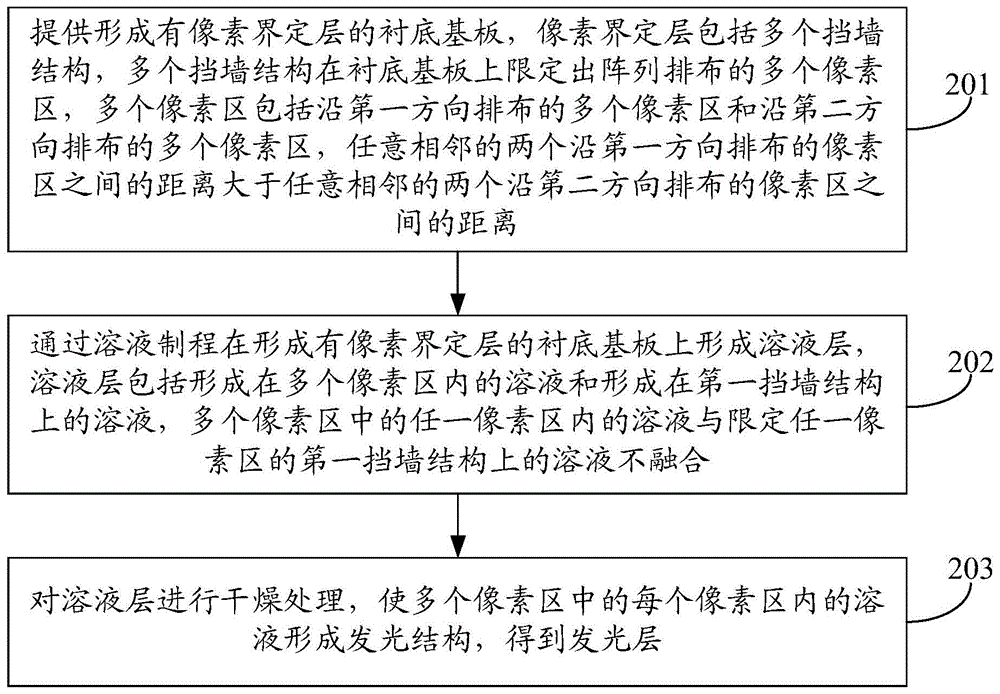
请参考图2,其示出了本发明实施例提供的一种发光层的制造方法的方法流程图,该发光层的制造方法可以用于制造电致发光器件中的发光层,参见图2,该方法包括:Please refer to FIG. 2 , which shows a method flowchart of a method for manufacturing a light-emitting layer provided by an embodiment of the present invention. The method for manufacturing a light-emitting layer can be used to manufacture a light-emitting layer in an electroluminescent device. Referring to FIG. 2 , The method includes:
步骤201、提供形成有像素界定层的衬底基板,像素界定层包括多个挡墙结构,多个挡墙结构在衬底基板上限定出阵列排布的多个像素区,多个像素区包括沿第一方向排布的多个像素区和沿第二方向排布的多个像素区,任意相邻的两个沿第一方向排布的像素区之间的距离大于任意相邻的两个沿第二方向排布的像素区之间的距离。
请参考图3,其示出了本发明实施例提供的一种形成有像素界定层011的衬底基板的示意图,参见图3,像素界定层011包括多个挡墙结构(图3中未标出),该多个挡墙结构在衬底基板(图3中未示出)上限定出阵列排布的多个像素区P,多个像素区P包括沿第一方向x排布的多个像素区P和沿第二方向y排布的多个像素区P,任意相邻的两个沿第一方向x排布的像素区P之间的距离x1大于任意相邻的两个沿第二方向y排布的像素区P之间的距离y1。如图3所示,在本发明实施例中,多个挡墙结构包括多个第一挡墙结构0111和多个第二挡墙结构0112,第一挡墙结构0111为多个挡墙结构中沿第一方向x排布的像素区P之间的挡墙结构,第二挡墙结构0112为多个挡墙结构中沿第二方向y排布的像素区P之间的挡墙结构,因此,任意相邻的两个沿第一方向x排布的像素区P之间的距离x1也即是第一挡墙结构0111的宽度,任意相邻的两个沿第二方向y排布的像素区P之间的距离y1也即是第二挡墙结构0112的宽度。Please refer to FIG. 3 , which is a schematic diagram of a base substrate provided with a
其中,衬底基板可以为透明衬底基板,其具体可以是采用玻璃、石英、透明树脂等具有一定坚固性的导光且非金属材料制成的衬底基板,或者,该衬底基板可以为采用聚酰亚胺(英文:polyimide;简称:PI)等材料制作的柔性衬底基板。像素界定层011可以采用疏水性透明树脂材料,通过一次构图工艺形成。具体地,可以采用涂覆、磁控溅射、热蒸发或者等离子体增强化学气相沉积法(英文:Plasma Enhanced Chemical Vapor Deposition,简称:PECVD)等方法在衬底基板上沉积一层疏水性透明树脂材料,得到树脂材料层,然后通过一次构图工艺对树脂材料层进行处理得到像素界定层011。其中,一次构图工艺包括光刻胶涂覆、曝光、显影、刻蚀和光刻胶剥离,因此,通过一次构图工艺对树脂材料层进行处理得到像素界定层011可以包括:在树脂材料层上涂覆一层具有一定厚度的光刻胶得到光刻胶层,采用掩膜版对光刻胶层进行曝光,使光刻胶层形成完全曝光区域和非曝光区域,之后采用显影工艺对光刻胶层进行处理,使完全曝光区域的光刻胶去除,非曝光区域的光刻胶保留,然后采用刻蚀工艺对树脂材料层上与完全曝光区域对应的区域进行刻蚀,以在树脂材料层上形成像素区,最后剥离非曝光区域的光刻胶得到如图3所示的像素界定层011。The substrate substrate may be a transparent substrate substrate, which may specifically be a substrate substrate made of a light-guiding and non-metallic material with certain sturdiness such as glass, quartz, transparent resin, or the like, or the substrate substrate may be The flexible substrate is made of materials such as polyimide (English: polyimide; abbreviation: PI). The
步骤202、通过溶液制程在形成有像素界定层的衬底基板上形成溶液层,溶液层包括形成在多个像素区内的溶液和形成在第一挡墙结构上的溶液,多个像素区中的任一像素区内的溶液与限定任一像素区的第一挡墙结构上的溶液不融合。Step 202: A solution layer is formed on the base substrate on which the pixel defining layer is formed through a solution process. The solution layer includes the solution formed in the plurality of pixel regions and the solution formed on the first retaining wall structure. The solution in any of the pixel regions is not fused with the solution on the first retaining wall structure defining any pixel region.
其中,溶液制程可以包括但不限于:喷墨打印制程、旋涂制程、丝网印刷制程、转印制程等。请参考图4,其示出了本发明实施例提供的一种在形成有像素界定层011的衬底基板上形成溶液层012后的示意图,结合图3和图4,溶液层012包括形成在多个像素区P内的溶液0121和形成在第一挡墙结构0111上的溶液0122,多个像素区P中的任一像素区P内的溶液0121与限定任一像素区P的第一挡墙结构0111上的溶液0122不融合。在本发明实施例中,像素界定层011的任一第一挡墙结构0111上的溶液的溶液量的取值范围包括:1皮升~200皮升,具体地,像素界定层011的任一第一挡墙结构0111上的溶液的溶液量的取值范围可以为10皮升~100皮升。需要说明的是,在本发明实施例中,像素界定层011的形成材料可以为疏水性透明树脂材料,这使得溶液在像素界定层011表面上的流动性较差,在形成溶液层012之后,如图4所示,像素区P内的溶液0121可以很好的位于像素区P内,第一挡墙结构0111上的溶液0122可以很好的位于第一挡墙结构0111上,并且,第一挡墙结构0111上的溶液0122可以呈半球形位于第一挡墙结构0111上。The solution process may include, but is not limited to, an inkjet printing process, a spin coating process, a screen printing process, a transfer printing process, and the like. Please refer to FIG. 4 , which shows a schematic diagram of forming a
在本发明实施例中,溶液层012可以通过一次溶液制程形成,也可以通过两次溶液制程形成。当通过一次溶液制程形成溶液层012时,可以通过一次溶液制程同时在像素区P内和第一挡墙结构0111上形成溶液;当通过两次溶液制程形成溶液层012时,可以先通过第一溶液制程在多个像素区P内形成溶液0121,然后通过第二溶液制程在第一挡墙结构0111上形成溶液0122,得到溶液层012。当然,也可以先通过第二溶液制程在第一挡墙结构0111上形成溶液0122,然后通过第一溶液制程在多个像素区P内形成溶液0121,本发明实施例对此不作限定。在本发明实施例中,第一溶液制程与第二溶液制程可以相同或不同,示例地,第一溶液制程包括喷墨打印制程,第二溶液制程包括喷墨打印制程和喷涂制程中的任意一种。需要说明的是,无论像素区P内的溶液与第一挡墙结构0111上的溶液是否通过一次溶液制程形成,该像素区P内的溶液与第一挡墙结构0111上的溶液可以为相同的溶液。In the embodiment of the present invention, the
步骤203、对溶液层进行干燥处理,使多个像素区中的每个像素区内的溶液形成发光结构,得到发光层。
可选地,可以采用减压干燥工艺对溶液层进行干燥处理,在此过程中,像素区内的溶剂挥发,溶质干燥形成发光结构,进而得到发光层。采用减压干燥工艺对溶液层进行干燥处理的过程具体可以包括:将形成有溶液层的衬底基板放置在密闭腔体内,然后对密闭腔体进行抽气,使密闭腔体内气压减小,以对溶液层进行干燥。需要说明的是,在采用减压干燥工艺对溶液层进行干燥处理的过程中,第一挡墙结构0111上的溶剂也会挥发,溶质也会干燥并留在第一挡墙结构0111上,但是对于电致发光器件而言,挡墙结构的存在不会对显示产生影响,因此该第一挡墙结构0111上的溶质也不会对显示产生影响。还需要说明的是,本发明实施例提供的减压干燥工艺的具体过程仅仅是示例性的,减压干燥工艺的具体实现过程可以参考相关技术,本发明实施例在此不再赘述。Optionally, the solution layer may be dried by a vacuum drying process. During this process, the solvent in the pixel area is volatilized, and the solute is dried to form a light-emitting structure, thereby obtaining a light-emitting layer. The process of drying the solution layer by using the reduced pressure drying process may specifically include: placing the substrate on which the solution layer is formed in a closed cavity, and then pumping air into the closed cavity to reduce the air pressure in the closed cavity, so as to reduce the air pressure in the closed cavity. The solution layer was dried. It should be noted that, in the process of drying the solution layer by the vacuum drying process, the solvent on the first retaining wall structure 0111 will also volatilize, and the solute will also be dried and remain on the first retaining wall structure 0111, but For the electroluminescent device, the existence of the barrier wall structure will not affect the display, so the solute on the first barrier wall structure 0111 will not affect the display either. It should also be noted that the specific process of the drying process under reduced pressure provided in the embodiment of the present invention is merely exemplary, and the specific implementation process of the drying process under reduced pressure may refer to the related art, which will not be repeated in the embodiment of the present invention.
需要说明的是,实际应用中,可以根据实际情况调整第一挡墙结构0111上的溶液量,使像素区中的溶剂能够在长轴方向上和短轴方向上相对平衡挥发,长轴方向上和短轴方向上的挥发气氛相对平衡,溶质能够在长轴方向上和短轴方向上分布相对均匀,保证形成的发光结构的厚度的均一性。本发明实施例提供的发光层的制造方法工艺过程简单,可以很好的优化发光层的性能。It should be noted that, in practical applications, the amount of solution on the first retaining wall structure 0111 can be adjusted according to the actual situation, so that the solvent in the pixel area can volatilize in a relative balance in the long-axis direction and the short-axis direction, and the long-axis direction Relatively balanced with the volatilization atmosphere in the short-axis direction, the solute can be relatively uniformly distributed in the long-axis direction and the short-axis direction, ensuring the uniformity of the thickness of the formed light-emitting structure. The manufacturing method of the light-emitting layer provided by the embodiment of the present invention has a simple process and can well optimize the performance of the light-emitting layer.
综上所述,本发明实施例提供的发光层的制造方法,由于第一挡墙结构上设置有溶液,该溶液可以保证在对溶液层进行干燥处理的过程中,像素区中的溶液在第一方向上受到的微作用力与在第二方向上受到的微作用力相同,使溶质在第一方向上的分布与在第二方向上的分布趋于相同,避免由于溶质分布不均匀导致发光结构的厚度的均一性较差,解决了发光层的均一性较差的问题,有助于提高发光层的均一性。To sum up, in the manufacturing method of the light-emitting layer provided by the embodiment of the present invention, since the first retaining wall structure is provided with a solution, the solution can ensure that during the drying process of the solution layer, the solution in the pixel area is The micro-action force received in one direction is the same as the micro-action force received in the second direction, so that the distribution of the solute in the first direction and the distribution in the second direction tend to be the same, avoiding luminescence due to uneven distribution of the solute The uniformity of the thickness of the structure is poor, which solves the problem of poor uniformity of the light-emitting layer and helps to improve the uniformity of the light-emitting layer.
请参考图5,其示出了本发明实施例提供的另一种发光层的制造方法的方法流程图,该发光层的制造方法可以用于制造电致发光器件中的发光层,参见图5,该方法包括:Please refer to FIG. 5 , which shows a method flow chart of another method for manufacturing a light-emitting layer provided by an embodiment of the present invention. The method for manufacturing a light-emitting layer can be used to manufacture a light-emitting layer in an electroluminescent device, see FIG. 5 , the method includes:
步骤501、提供形成有像素界定层的衬底基板,像素界定层包括多个挡墙结构,多个挡墙结构在衬底基板上限定出阵列排布的多个像素区,多个像素区包括沿第一方向排布的多个像素区和沿第二方向排布的多个像素区,任意相邻的两个沿第一方向排布的像素区之间的距离大于任意相邻的两个沿第二方向排布的像素区之间的距离。Step 501: Provide a base substrate on which a pixel definition layer is formed, the pixel definition layer includes a plurality of retaining wall structures, and the plurality of retaining wall structures define a plurality of pixel regions arranged in an array on the base substrate, and the plurality of pixel regions include: For the plurality of pixel areas arranged along the first direction and the plurality of pixel areas arranged along the second direction, the distance between any two adjacent pixel areas arranged along the first direction is greater than any adjacent two pixel areas The distance between the pixel regions arranged along the second direction.
该步骤501的具体实现过程可以参考图2所示实施例中的步骤201,本实施例在此不再赘述。For a specific implementation process of this step 501, reference may be made to step 201 in the embodiment shown in FIG. 2, and details are not described herein again in this embodiment.
步骤502、通过溶液制程在形成有像素界定层的衬底基板上形成溶液层,溶液层包括形成在多个像素区内的溶液、形成在第一挡墙结构上的溶液和形成在第二挡墙结构上的溶液,多个像素区中的任一像素区内的溶液与限定任一像素区的第一挡墙结构上的溶液不融合,且与限定任一像素区的第二挡墙结构上的溶液不融合,第二挡墙结构上的溶液的溶液量小于第一挡墙结构上的溶液的溶液量。Step 502: A solution layer is formed on the base substrate on which the pixel defining layer is formed by a solution process, the solution layer includes the solution formed in the plurality of pixel regions, the solution formed on the first retaining wall structure, and the solution formed in the second retaining wall structure. The solution on the wall structure, the solution in any pixel region of the plurality of pixel regions is not fused with the solution on the first retaining wall structure defining any pixel region, and is not fused with the second retaining wall structure defining any pixel region The solution on the second retaining wall structure is not fused, and the solution amount of the solution on the second retaining wall structure is smaller than the solution amount of the solution on the first retaining wall structure.
其中,溶液制程可以包括但不限于:喷墨打印制程、旋涂制程、丝网印刷制程、转印制程等。请参考图6,其示出了本发明实施例提供的一种在形成有像素界定层011的衬底基板上形成溶液层012后的示意图,结合图3和图6,溶液层012包括形成在多个像素区P内的溶液0121、形成在第一挡墙结构0111上的溶液0122和形成在第二挡墙结构0112上的溶液0123,多个像素区P中的任一像素区P内的溶液0121与限定任一像素区P的第一挡墙结构0111上的溶液0122不融合,且多个像素区P中的任一像素区P内的溶液0121与限定任一像素区P的第二挡墙结构0112上的溶液0123不融合。需要说明的是,在本发明实施例中,像素界定层011的形成材料可以为疏水性透明树脂材料,这使得溶液在像素界定层011表面上的流动性较差,在形成溶液层012之后,结合图3和图6,像素区P内的溶液0121可以很好的位于像素区P内,第一挡墙结构0111上的溶液0122可以很好的位于第一挡墙结构0111上,第二挡墙结构0112上的溶液0123可以很好的位于第二挡墙结构0112上,并且,第一挡墙结构0111上的溶液0122可以呈半球形位于第一挡墙结构0111上,第二挡墙结构0112上的溶液0123可以呈半球形位于第二挡墙结构0112上。The solution process may include, but is not limited to, an inkjet printing process, a spin coating process, a screen printing process, a transfer printing process, and the like. Please refer to FIG. 6 , which shows a schematic diagram of forming a
在本发明实施例中,溶液层012可以通过一次溶液制程形成、也可以通过两次溶液制程形成,还可以通过三次溶液制程形成。当通过一次溶液制程形成溶液层012时,可以通过一次溶液制程同时在像素区P内、第一挡墙结构0111上和第二挡墙结构0112上形成溶液;当通过两次溶液制程形成溶液层012时,可以先通过第一溶液制程在多个像素区P内形成溶液0121,然后通过第二溶液制程在第一挡墙结构0111上形成溶液0122,并在第二挡墙结构0112上形成溶液0123,得到溶液层012;当通过三次溶液制程形成溶液层012时,可以先通过第一溶液制程在多个像素区P内形成溶液0121,然后通过第二溶液制程在第一挡墙结构0111上形成溶液0122,最后通过第三溶液制程在第二挡墙结构0112上形成溶液0123,得到溶液层012。当然,实际应用中,在像素区P内形成溶液0121、在第一挡墙结构0111上形成溶液0122以及在第二挡墙结构0112上形成溶液0123的过程可以颠倒,本发明实施例不对溶液0121、溶液0122和溶液0123的形成顺序进行限定。需要说明的是,无论像素区P内的溶液、第一挡墙结构0111上的溶液和第二挡墙结构0112上的溶液是否通过一次溶液制程形成,该像素区P内的溶液、第一挡墙结构0111上的溶液和第二挡墙结构0112上的溶液可以为相同的溶液。In the embodiment of the present invention, the
步骤503、对溶液层进行干燥处理,使多个像素区中的每个像素区内的溶液形成发光结构,得到发光层。
该步骤503的具体实现过程可以参考图2所示实施例中的步骤203,本实施例在此不再赘述。但是需要说明的是,在采用减压干燥工艺对溶液层012进行干燥处理的过程中,第二挡墙结构0112上的溶剂也会挥发,溶质也会干燥并留在第二挡墙结构0112上,而对于电致发光器件而言,挡墙结构的存在不会对显示产生影响,因此该第二挡墙结构0112上的溶质也不会对显示产生影响。For the specific implementation process of this
需要说明的是,实际应用中,可以根据实际情况调整第一挡墙结构0111上的溶液量和第二挡墙结构0112上的溶液量,使像素区中的溶剂能够在长轴方向上和短轴方向上相对平衡挥发,长轴方向上和短轴方向上的挥发气氛相对平衡,溶质能够在长轴方向上和短轴方向上分布相对均匀,保证形成的发光结构的厚度的均一性。本发明实施例提供的发光层的制造方法工艺过程简单,可以很好的优化发光层的性能。It should be noted that, in practical applications, the amount of solution on the first retaining wall structure 0111 and the amount of solution on the second retaining wall structure 0112 can be adjusted according to the actual situation, so that the solvent in the pixel area can be Relatively balanced volatilization in the axial direction, relatively balanced volatilization atmosphere in the long-axis direction and short-axis direction, solutes can be relatively uniformly distributed in the long-axis direction and the short-axis direction, ensuring the uniformity of the thickness of the formed light-emitting structure. The manufacturing method of the light-emitting layer provided by the embodiment of the present invention has a simple process and can well optimize the performance of the light-emitting layer.
综上所述,本发明实施例提供的发光层的制造方法,由于第一挡墙结构上设置有溶液,该溶液可以保证在对溶液层进行干燥处理的过程中,像素区中的溶液在第一方向上受到的微作用力与在第二方向上受到的微作用力相同,使溶质在第一方向上的分布与在第二方向上的分布趋于相同,避免由于溶质分布不均匀导致发光结构的厚度的均一性较差,解决了发光层的均一性较差的问题,有助于提高发光层的均一性。To sum up, in the manufacturing method of the light-emitting layer provided by the embodiment of the present invention, since the first retaining wall structure is provided with a solution, the solution can ensure that during the drying process of the solution layer, the solution in the pixel area is The micro-action force received in one direction is the same as the micro-action force received in the second direction, so that the distribution of the solute in the first direction and the distribution in the second direction tend to be the same, avoiding luminescence due to uneven distribution of the solute The uniformity of the thickness of the structure is poor, which solves the problem of poor uniformity of the light-emitting layer and helps to improve the uniformity of the light-emitting layer.
请参考图7,其示出了本发明实施例提供的再一种发光层的制造方法的方法流程图,该发光层的制造方法可以用于制造电致发光器件中的发光层,参见图7,该方法包括:Please refer to FIG. 7 , which shows a method flowchart of another method for manufacturing a light-emitting layer provided by an embodiment of the present invention. The method for manufacturing a light-emitting layer can be used to manufacture a light-emitting layer in an electroluminescent device, see FIG. 7 , the method includes:
步骤701、提供形成有像素界定层的衬底基板,像素界定层包括多个挡墙结构,多个挡墙结构在衬底基板上限定出阵列排布的多个像素区,多个像素区包括沿第一方向排布的多个像素区和沿第二方向排布的多个像素区,任意相邻的两个沿第一方向排布的像素区之间的距离大于任意相邻的两个沿第二方向排布的像素区之间的距离。
该步骤701的具体实现过程可以参考图2所示实施例中的步骤201,本实施例在此不再赘述。For the specific implementation process of this
步骤702、通过一次构图工艺对像素界定层进行处理,使第一挡墙结构上形成第一凹槽。Step 702: Process the pixel defining layer through a patterning process to form a first groove on the first retaining wall structure.
请参考图8和图9,其示出了本发明实施例提供的两种在第一挡墙结构(图8中未标出)上形成第一凹槽G1后的示意图,参见图8,第一凹槽G1的开口面的形状为圆形,或者,参见图9,第一凹槽G1的开口面的形状为方形,且如图9所示,当第一凹槽G1的开口面的形状为方形时,沿第二方向y排布的多个像素区P中,位于任意相邻的两个像素区P同一侧的两个第一挡墙结构0111上的第一凹槽G1可以为同一凹槽。Please refer to FIG. 8 and FIG. 9 , which show two schematic diagrams after the first groove G1 is formed on the first retaining wall structure (not shown in FIG. 8 ) according to an embodiment of the present invention. The shape of the opening surface of a groove G1 is circular, or, referring to FIG. 9 , the shape of the opening surface of the first groove G1 is square, and as shown in FIG. 9 , when the shape of the opening surface of the first groove G1 is square When it is a square, among the plurality of pixel regions P arranged along the second direction y, the first grooves G1 on the two first retaining wall structures 0111 located on the same side of any adjacent two pixel regions P may be the same. groove.
在本发明实施例中,结合图3、图8和图9,可以通过一次构图工艺对像素界定层011进行处理,使第一挡墙结构0111上形成第一凹槽G1,该第一凹槽G1与像素区P之间具有一定距离,以避免后续形成溶液层之后,第一凹槽G1内的溶液与像素区P内的溶液融合。其中,一次构图工艺包括光刻胶涂覆、曝光、显影、刻蚀和光刻胶剥离,因此,通过一次构图工艺对像素界定层011进行处理,使第一挡墙结构0111上形成第一凹槽G1可以包括:在像素界定层011的挡墙结构上涂覆一层具有一定厚度的光刻胶得到光刻胶层,采用掩膜版对光刻胶层进行曝光,使光刻胶层形成完全曝光区域和非曝光区域,之后采用显影工艺对光刻胶层进行处理,使完全曝光区域的光刻胶去除,非曝光区域的光刻胶保留,然后采用刻蚀工艺对像素界定层011上(也即是第一挡墙结构0111上)与完全曝光区域对应的区域进行刻蚀,以在像素界定层011上形成第一凹槽G1,最后剥离非曝光区域的光刻胶得到如图8或图9所示的结构。其中,可以采用半刻蚀工艺对第一凹槽G1对应的区域进行刻蚀,以避免将像素界定层011刻透,进而避免像素界定层011下方的晶体管电路裸露。In the embodiment of the present invention, referring to FIG. 3 , FIG. 8 and FIG. 9 , the
需要说明的是,在本发明实施例中,第一凹槽G1与像素区P可以通过同一次构图工艺形成,此时,可以采用涂覆、磁控溅射、热蒸发或者PECVD等方法在衬底基板上沉积一层疏水性透明树脂材料,得到树脂材料层,然后通过一次构图工艺对树脂材料层进行处理得到像素界定层011,该像素界定层011包括阵列排布的多个像素区P,且第一挡墙结构0111上形成有第一凹槽G1。It should be noted that, in the embodiment of the present invention, the first groove G1 and the pixel region P may be formed through the same patterning process. A layer of hydrophobic transparent resin material is deposited on the base substrate to obtain a resin material layer, and then the resin material layer is processed through a patterning process to obtain a
步骤703、通过溶液制程在形成有像素界定层的衬底基板上形成溶液层,溶液层包括形成在多个像素区内的溶液和形成在第一凹槽内的溶液。
该步骤703的具体实现过程可以参考图2所示实施例中的步骤202,本实施例在此不再赘述。但是需要说明的是,对于图9所示的像素界定层,如图10所示,可以采用喷嘴涂覆设备02沿第一凹槽G1的长度方向,在第一凹槽G1内涂覆溶液,以在第一凹槽G1内形成溶液,然后再采用溶液制程(例如,喷墨打印制程)在像素区P内充填溶液,以在形成有像素界定层的衬底基板上形成溶液层。需要说明的是,本发明实施例通过在第一挡墙结构上形成第一凹槽G1,该第一凹槽G1可以将溶液限定在第一挡墙结构的固定位置,避免溶液在第一挡墙结构上流动。For the specific implementation process of
步骤704、对溶液层进行干燥处理,使多个像素区中的每个像素区内的溶液形成发光结构,得到发光层。
该步骤704的具体实现过程可以参考图5所示实施例中的步骤503,本实施例在此不再赘述。但是需要说明的是,在采用减压干燥工艺对溶液层进行干燥处理的过程中,第一凹槽G1内的溶剂也会挥发,溶质也会干燥并留在第一凹槽G1内,但是由于第一凹槽G1位于第一挡墙结构0111上,而对于电致发光器件而言,挡墙结构的存在不会对显示产生影响,因此该第一凹槽G1内的溶质也不会对显示产生影响。For the specific implementation process of
还需要说明的是,本发明实施例是以在第一挡墙结构上形成凹槽为例进行说明的,实际应用中,对于图5所示的情况,还可以在第二挡墙结构上形成凹槽,以便于在第二挡墙结构上形成溶液,本发明实施例在此不再赘述。It should also be noted that the embodiment of the present invention is described by taking the formation of grooves on the first retaining wall structure as an example. In practical applications, for the situation shown in FIG. 5 , the grooves can also be formed on the second retaining wall structure. A groove is formed so as to form a solution on the second retaining wall structure, which is not repeated in this embodiment of the present invention.
综上所述,本发明实施例提供的发光层的制造方法,由于第一挡墙结构上设置有溶液,该溶液可以保证在对溶液层进行干燥处理的过程中,像素区中的溶液在第一方向上受到的微作用力与在第二方向上受到的微作用力相同,使溶质在第一方向上的分布与在第二方向上的分布趋于相同,避免由于溶质分布不均匀导致发光结构的厚度的均一性较差,解决了发光层的均一性较差的问题,有助于提高发光层的均一性。To sum up, in the manufacturing method of the light-emitting layer provided by the embodiment of the present invention, since the first retaining wall structure is provided with a solution, the solution can ensure that during the drying process of the solution layer, the solution in the pixel area is The micro-action force received in one direction is the same as the micro-action force received in the second direction, so that the distribution of the solute in the first direction and the distribution in the second direction tend to be the same, avoiding luminescence due to uneven distribution of the solute The uniformity of the thickness of the structure is poor, which solves the problem of poor uniformity of the light-emitting layer and helps to improve the uniformity of the light-emitting layer.
请参考图11,其示出了本发明实施例提供的又一种发光层的制造方法的方法流程图,该发光层的制造方法可以用于制造电致发光器件中的发光层,参见图11,该方法包括:Please refer to FIG. 11 , which shows a method flowchart of another method for manufacturing a light-emitting layer provided by an embodiment of the present invention. The method for manufacturing a light-emitting layer can be used to manufacture a light-emitting layer in an electroluminescent device, see FIG. 11 , the method includes:
步骤1101、提供形成有像素界定层的衬底基板,像素界定层包括多个挡墙结构,多个挡墙结构在衬底基板上限定出阵列排布的多个像素区,多个像素区包括沿第一方向排布的多个像素区和沿第二方向排布的多个像素区,任意相邻的两个沿第一方向排布的像素区之间的距离大于任意相邻的两个沿第二方向排布的像素区之间的距离。
步骤1102、通过一次构图工艺对像素界定层进行处理,使第一挡墙结构上形成第一凹槽。
该步骤1101和步骤1102的具体实现过程可以参考图7所示实施例中的步骤701和步骤702,本实施例在此不再赘述。For the specific implementation process of the
步骤1103、通过一次构图工艺对像素界定层进行处理,使沿第二方向排布的多个像素区中,位于任意相邻的两个像素区同一侧的两个第一挡墙结构上的第一凹槽之间形成第二凹槽,位于任意相邻的两个像素区同一侧的两个第一挡墙结构上的第一凹槽通过第二凹槽连通。Step 1103: Process the pixel defining layer through a patterning process, so that in the plurality of pixel regions arranged along the second direction, the first block on the two first retaining wall structures located on the same side of any adjacent two pixel regions. A second groove is formed between a groove, and the first grooves on the two first blocking wall structures located on the same side of any two adjacent pixel regions are communicated through the second grooves.
请参考图12,其示出了本发明实施例提供的一种第一凹槽通过第二凹槽连通的示意图,参见图12,第一凹槽G1的开口面的形状为圆形,沿第二方向y排布的多个像素区P中,位于任意相邻的两个像素区P同一侧的两个第一挡墙结构(图12中未示出)上的第一凹槽G1之间形成有第二凹槽G2,位于任意相邻的两个像素区P同一侧的两个第一挡墙结构上的第一凹槽G1通过第二凹槽G2连通。在本发明实施例中,第一凹槽G1的深度可以大于或等于第二凹槽G2的深度,第一凹槽G1的开口面的面积可以大于第二凹槽G2的开口面的面积,这样可以保证形成溶液层之后,第一凹槽G1内的溶液量大于第二凹槽G2内的溶液量,凹槽内的溶液更多的停留在与像素区正对的凹槽内,以更好的调节最终形成的发光结构的均一性。Please refer to FIG. 12 , which shows a schematic diagram of a first groove communicating with a second groove according to an embodiment of the present invention. Referring to FIG. 12 , the shape of the opening surface of the first groove G1 is a circle. Among the plurality of pixel regions P arranged in two directions y, between the first grooves G1 on the two first retaining wall structures (not shown in FIG. 12 ) on the same side of any two adjacent pixel regions P A second groove G2 is formed, and the first grooves G1 on the two first retaining wall structures located on the same side of any two adjacent pixel regions P are communicated with each other through the second groove G2. In this embodiment of the present invention, the depth of the first groove G1 may be greater than or equal to the depth of the second groove G2, and the area of the opening surface of the first groove G1 may be greater than the area of the opening surface of the second groove G2, so that It can be ensured that after the solution layer is formed, the amount of solution in the first groove G1 is greater than that in the second groove G2, and more of the solution in the groove stays in the groove opposite to the pixel area, so as to better The uniformity of the final formed light-emitting structure is adjusted.
在本发明实施例中,结合图3、图8和图12,可以通过一次构图工艺对像素界定层011进行处理,使沿第二方向y排布的多个像素区P中,位于任意相邻的两个像素区P同一侧的两个第一挡墙结构011上的第一凹槽G1之间形成第二凹槽G2。具体通过一次构图工艺对像素界定层011进行处理的过程可以参考图7所示实施例中的步骤702,本实施例在此不再赘述。In this embodiment of the present invention, referring to FIG. 3 , FIG. 8 and FIG. 12 , the
需要说明的是,在本发明实施例中,第一凹槽G1、第二凹槽G2以及像素区P三者可以通过同一次构图工艺形成,此时,可以采用涂覆、磁控溅射、热蒸发或者PECVD等方法在衬底基板上沉积一层疏水性透明树脂材料,得到树脂材料层,然后通过一次构图工艺对树脂材料层进行处理得到像素界定层011,该像素界定层011包括阵列排布的多个像素区P,第一挡墙结构0111上形成有第一凹槽G1,沿第二方向y排布的多个像素区P中,位于任意相邻的两个像素区P同一侧的两个第一挡墙结构011上的第一凹槽G1之间形成有第二凹槽G2。It should be noted that, in the embodiment of the present invention, the first groove G1, the second groove G2 and the pixel region P can be formed through the same patterning process. At this time, coating, magnetron sputtering, A layer of hydrophobic transparent resin material is deposited on the base substrate by thermal evaporation or PECVD to obtain a resin material layer, and then the resin material layer is processed through a patterning process to obtain a
步骤1104、通过溶液制程在形成有像素界定层的衬底基板上形成溶液层,溶液层包括形成在多个像素区内的溶液、形成在第一凹槽内的溶液和形成在第二凹槽内的溶液。
该步骤1104的具体实现过程可以参考图2所示实施例中的步骤202,本实施例在此不再赘述。但是需要说明的是,对于图12所示的像素界定层,可以采用喷嘴涂覆设备在第一凹槽G1和第二凹槽G2内涂覆溶液,以在第一凹槽G1和第二凹槽G2内形成溶液,然后再采用溶液制程(例如,喷墨打印制程)在像素区P内充填溶液,以在形成有像素界定层的衬底基板上形成溶液层。For the specific implementation process of this
步骤1105、对溶液层进行干燥处理,使多个像素区中的每个像素区内的溶液形成发光结构,得到发光层。
该步骤704的具体实现过程可以参考图5所示实施例中的步骤503,本实施例在此不再赘述。但是需要说明的是,在采用减压干燥工艺对溶液层进行干燥处理的过程中,第一凹槽G1和第二凹槽G2内的溶剂也会挥发,溶质也会干燥并留在第一凹槽G1和第二凹槽G2内,但是由于第一凹槽G1和第二凹槽G2均位于挡墙结构上,而对于电致发光器件而言,挡墙结构的存在不会对显示产生影响,因此该第一凹槽G1内的溶质和第二凹槽G2内的溶质也不会对显示产生影响。For the specific implementation process of
还需要说明的是,本发明实施例是以在第一挡墙结构上形成凹槽为例进行说明的,实际应用中,对于图6所示的情况,还可以在第二挡墙结构上形成凹槽,且第二挡墙结构上形成凹槽可以连通,以便于在第二挡墙结构上形成溶液,本发明实施例在此不再赘述。It should also be noted that the embodiment of the present invention is described by taking the formation of grooves on the first retaining wall structure as an example. In practical applications, for the situation shown in FIG. 6 , the grooves can also be formed on the second retaining wall structure. The grooves formed on the second retaining wall structure can communicate with each other, so as to facilitate the formation of a solution on the second retaining wall structure, which is not repeated in this embodiment of the present invention.
综上所述,本发明实施例提供的发光层的制造方法,由于第一挡墙结构上设置有溶液,该溶液可以保证在对溶液层进行干燥处理的过程中,像素区中的溶液在第一方向上受到的微作用力与在第二方向上受到的微作用力相同,使溶质在第一方向上的分布与在第二方向上的分布趋于相同,避免由于溶质分布不均匀导致发光结构的厚度的均一性较差,解决了发光层的均一性较差的问题,有助于提高发光层的均一性。To sum up, in the manufacturing method of the light-emitting layer provided by the embodiment of the present invention, since the first retaining wall structure is provided with a solution, the solution can ensure that during the drying process of the solution layer, the solution in the pixel area is The micro-action force received in one direction is the same as the micro-action force received in the second direction, so that the distribution of the solute in the first direction and the distribution in the second direction tend to be the same, avoiding luminescence due to uneven distribution of the solute The uniformity of the thickness of the structure is poor, which solves the problem of poor uniformity of the light-emitting layer and helps to improve the uniformity of the light-emitting layer.
本发明实施例还提供了一种电致发光器件,该电致发光器件包括:采用图2、图5、图7和图11任一所示的方法制造的发光层。An embodiment of the present invention further provides an electroluminescent device, the electroluminescent device comprising: a light-emitting layer manufactured by using any of the methods shown in FIG. 2 , FIG. 5 , FIG. 7 and FIG. 11 .
当然,实际应用中,该电致发光器件还包括TFT层、阳极层、PDL和阴极层,TFT层、阳极层和PDL依次叠加,且TFT层、阳极层和PDL位于发光层与衬底基板之间,阴极层位于发光层的上方,TFT层包括多个TFT,阳极层包括多个阳极结构,TFT、阳极结构和发光层的发光结构三者一一对应。其中,关于电致发光器件的具体结构,请参考相关技术,本发明实施例提供的电致发光器件的发光层的均一性较好,从而,该电致发光器件具有较好的显示效果以及较长的使用寿命。Of course, in practical applications, the electroluminescent device also includes a TFT layer, an anode layer, a PDL, and a cathode layer. The TFT layer, the anode layer, and the PDL are stacked in sequence, and the TFT layer, the anode layer, and the PDL are located between the light-emitting layer and the substrate. In the meantime, the cathode layer is located above the light-emitting layer, the TFT layer includes a plurality of TFTs, the anode layer includes a plurality of anode structures, and the TFTs, the anode structures and the light-emitting structures of the light-emitting layer correspond one-to-one. For the specific structure of the electroluminescent device, please refer to the related art. The uniformity of the light-emitting layer of the electroluminescent device provided by the embodiment of the present invention is good, so the electroluminescent device has better display effect and relatively Long service life.
本发明实施例还提供了一种显示装置,该显示装置包括上述电致发光器件。该显示装置可以为OLED显示面板、手机、平板电脑、电视机、显示器、笔记本电脑、数码相框或导航仪等任何具有显示功能的产品或部件。An embodiment of the present invention further provides a display device, which includes the above electroluminescent device. The display device can be any product or component with a display function, such as an OLED display panel, a mobile phone, a tablet computer, a TV, a monitor, a notebook computer, a digital photo frame or a navigator.
本发明中术语“和/或”,仅仅是一种描述关联对象的关联关系,表示可以存在三种关系,例如,A和/或B,可以表示:单独存在A,同时存在A和B,单独存在B这三种情况。另外,本文中字符“/”,一般表示前后关联对象是一种“或”的关系。The term "and/or" in the present invention is only an association relationship to describe associated objects, indicating that there can be three kinds of relationships, for example, A and/or B, it can mean that A exists alone, A and B exist at the same time, independently There are three cases of B. In addition, the character "/" in this document generally indicates that the related objects are an "or" relationship.
本领域普通技术人员可以理解实现上述实施例的全部或部分步骤可以通过硬件来完成,也可以通过程序来指令相关的硬件完成,所述的程序可以存储于一种计算机可读存储介质中,上述提到的存储介质可以是只读存储器,磁盘或光盘等。Those of ordinary skill in the art can understand that all or part of the steps of implementing the above embodiments can be completed by hardware, or can be completed by instructing relevant hardware through a program, and the program can be stored in a computer-readable storage medium. The storage medium mentioned may be a read-only memory, a magnetic disk or an optical disk, etc.
以上所述仅为本发明的较佳实施例,并不用以限制本发明,凡在本发明的精神和原则之内,所作的任何修改、等同替换、改进等,均应包含在本发明的保护范围之内。The above are only preferred embodiments of the present invention and are not intended to limit the present invention. Any modifications, equivalent replacements, improvements, etc. made within the spirit and principles of the present invention shall be included in the protection of the present invention. within the range.
Claims (12)
Priority Applications (6)
| Application Number | Priority Date | Filing Date | Title |
|---|---|---|---|
| CN201710758714.2A CN109427847B (en) | 2017-08-29 | 2017-08-29 | Manufacturing method of light-emitting layer, electroluminescent device and display device |
| JP2018561620A JP7091257B2 (en) | 2017-08-29 | 2018-04-10 | Manufacturing method of light emitting layer, electroluminescent device and display device |
| PCT/CN2018/082521 WO2019041820A1 (en) | 2017-08-29 | 2018-04-10 | Manufacturing method for light-emitting layer, electroluminescent device and display device |
| US16/303,482 US11227904B2 (en) | 2017-08-29 | 2018-04-10 | Method for manufacturing light-emitting layer, electroluminescent device and display device |
| EP18803306.2A EP3678181B1 (en) | 2017-08-29 | 2018-04-10 | Manufacturing method for light-emitting layer, electroluminescent device and display device |
| KR1020187035925A KR102223517B1 (en) | 2017-08-29 | 2018-04-10 | Method for manufacturing light emitting layer, electroluminescent device and display device |
Applications Claiming Priority (1)
| Application Number | Priority Date | Filing Date | Title |
|---|---|---|---|
| CN201710758714.2A CN109427847B (en) | 2017-08-29 | 2017-08-29 | Manufacturing method of light-emitting layer, electroluminescent device and display device |
Publications (2)
| Publication Number | Publication Date |
|---|---|
| CN109427847A CN109427847A (en) | 2019-03-05 |
| CN109427847B true CN109427847B (en) | 2020-12-11 |
Family
ID=65503856
Family Applications (1)
| Application Number | Title | Priority Date | Filing Date |
|---|---|---|---|
| CN201710758714.2A Active CN109427847B (en) | 2017-08-29 | 2017-08-29 | Manufacturing method of light-emitting layer, electroluminescent device and display device |
Country Status (6)
| Country | Link |
|---|---|
| US (1) | US11227904B2 (en) |
| EP (1) | EP3678181B1 (en) |
| JP (1) | JP7091257B2 (en) |
| KR (1) | KR102223517B1 (en) |
| CN (1) | CN109427847B (en) |
| WO (1) | WO2019041820A1 (en) |
Families Citing this family (6)
| Publication number | Priority date | Publication date | Assignee | Title |
|---|---|---|---|---|
| CN109887978B (en) * | 2019-03-12 | 2021-01-12 | 京东方科技集团股份有限公司 | Display substrate, manufacturing method thereof and display device |
| CN111883657B (en) * | 2019-07-29 | 2023-09-05 | 广东聚华印刷显示技术有限公司 | Display device and manufacturing method thereof |
| CN113540188B (en) * | 2021-06-29 | 2024-05-14 | 上海天马微电子有限公司 | Display substrate and display panel |
| KR20230050547A (en) * | 2021-10-07 | 2023-04-17 | 삼성디스플레이 주식회사 | Display device |
| CN113991031B (en) * | 2021-10-27 | 2023-05-23 | 京东方科技集团股份有限公司 | Display panel, preparation method thereof and display device |
| CN115449747B (en) * | 2022-10-19 | 2024-02-13 | 云谷(固安)科技有限公司 | Precision mask and production method thereof |
Citations (3)
| Publication number | Priority date | Publication date | Assignee | Title |
|---|---|---|---|---|
| JP2005276479A (en) * | 2004-03-23 | 2005-10-06 | Seiko Epson Corp | ELECTRO-OPTICAL DEVICE, MANUFACTURING METHOD THEREOF, AND ELECTRONIC DEVICE |
| CN102388673A (en) * | 2010-06-30 | 2012-03-21 | 松下电器产业株式会社 | Organic el display panel and method for manufacturing same |
| CN104882468A (en) * | 2015-06-09 | 2015-09-02 | 京东方科技集团股份有限公司 | Organic electroluminescence display base plate and manufacturing method thereof, and display apparatus |
Family Cites Families (16)
| Publication number | Priority date | Publication date | Assignee | Title |
|---|---|---|---|---|
| JP2004230209A (en) | 2003-01-28 | 2004-08-19 | Casio Comput Co Ltd | Solution ejection device |
| JP4297106B2 (en) * | 2005-02-23 | 2009-07-15 | セイコーエプソン株式会社 | Film pattern forming method, device manufacturing method, electro-optical device, and electronic apparatus |
| CN100405092C (en) * | 2005-06-17 | 2008-07-23 | 虹创科技股份有限公司 | Color filter and its preparation method |
| KR101152140B1 (en) | 2005-08-11 | 2012-06-15 | 삼성전자주식회사 | Display device and method of making display device |
| KR101325577B1 (en) | 2006-04-28 | 2013-11-06 | 삼성디스플레이 주식회사 | Organic electro luminescence device and method of manufacturing the same |
| WO2009084209A1 (en) | 2007-12-28 | 2009-07-09 | Panasonic Corporation | Organic el device, organic el display panel, and method for manufacturing the organic el device |
| WO2013080490A1 (en) | 2011-12-02 | 2013-06-06 | パナソニック株式会社 | Organic electroluminescence display panel and method of manufacturing same |
| KR101851679B1 (en) | 2011-12-19 | 2018-04-25 | 삼성디스플레이 주식회사 | Organic light emitting display device and the fabrication method thereof |
| CN102705790B (en) * | 2012-03-16 | 2014-08-27 | 京东方科技集团股份有限公司 | Light-emitting diode display back plate, manufacturing method and display device for light-emitting diode display back plate |
| KR102000709B1 (en) * | 2012-08-31 | 2019-09-30 | 삼성디스플레이 주식회사 | Manufacturing method of a display panel |
| KR101997571B1 (en) | 2012-10-08 | 2019-07-09 | 삼성디스플레이 주식회사 | Organic light emitting display and method of manufacturing the same |
| CN103311269B (en) * | 2013-05-29 | 2017-06-09 | 京东方科技集团股份有限公司 | A kind of OLED pixel limiting structure and preparation method thereof |
| KR102181978B1 (en) | 2014-08-22 | 2020-11-24 | 삼성디스플레이 주식회사 | Light emitting display device and method of manufacturing the same |
| CN104299968B (en) * | 2014-09-22 | 2017-04-26 | 京东方科技集团股份有限公司 | Electroluminescent device, manufacturing method of electroluminescent device, display substrate and display device |
| JP2016126860A (en) | 2014-12-26 | 2016-07-11 | ソニー株式会社 | Display device, method of manufacturing the same, and electronic equipment |
| WO2017135227A1 (en) | 2016-02-01 | 2017-08-10 | シャープ株式会社 | Organic el display device |
-
2017
- 2017-08-29 CN CN201710758714.2A patent/CN109427847B/en active Active
-
2018
- 2018-04-10 US US16/303,482 patent/US11227904B2/en active Active
- 2018-04-10 EP EP18803306.2A patent/EP3678181B1/en active Active
- 2018-04-10 JP JP2018561620A patent/JP7091257B2/en active Active
- 2018-04-10 WO PCT/CN2018/082521 patent/WO2019041820A1/en not_active Ceased
- 2018-04-10 KR KR1020187035925A patent/KR102223517B1/en active Active
Patent Citations (3)
| Publication number | Priority date | Publication date | Assignee | Title |
|---|---|---|---|---|
| JP2005276479A (en) * | 2004-03-23 | 2005-10-06 | Seiko Epson Corp | ELECTRO-OPTICAL DEVICE, MANUFACTURING METHOD THEREOF, AND ELECTRONIC DEVICE |
| CN102388673A (en) * | 2010-06-30 | 2012-03-21 | 松下电器产业株式会社 | Organic el display panel and method for manufacturing same |
| CN104882468A (en) * | 2015-06-09 | 2015-09-02 | 京东方科技集团股份有限公司 | Organic electroluminescence display base plate and manufacturing method thereof, and display apparatus |
Also Published As
| Publication number | Publication date |
|---|---|
| EP3678181A4 (en) | 2021-07-14 |
| JP2020532041A (en) | 2020-11-05 |
| JP7091257B2 (en) | 2022-06-27 |
| EP3678181A1 (en) | 2020-07-08 |
| WO2019041820A1 (en) | 2019-03-07 |
| EP3678181B1 (en) | 2023-03-29 |
| KR102223517B1 (en) | 2021-03-05 |
| CN109427847A (en) | 2019-03-05 |
| US20210225966A1 (en) | 2021-07-22 |
| KR20190033476A (en) | 2019-03-29 |
| US11227904B2 (en) | 2022-01-18 |
Similar Documents
| Publication | Publication Date | Title |
|---|---|---|
| CN109427847B (en) | Manufacturing method of light-emitting layer, electroluminescent device and display device | |
| US11004917B2 (en) | Pixel defining layer, display substrate and manufacturing method thereof, and display apparatus | |
| JP6910958B2 (en) | Display board and manufacturing method of display board | |
| JP6219685B2 (en) | Luminescent display backplane, display device, and pixel definition layer manufacturing method | |
| US10957751B2 (en) | Pixel defining layer and manufacturing method thereof, display substrate, display panel | |
| US11127798B2 (en) | Pixel definition layer and manufacturing method thereof, display substrate, and display panel | |
| CN105118845B (en) | Organic electroluminescent display substrate and preparation method, display panel, and display device | |
| CN110085655B (en) | Display panel, manufacturing method thereof and display device | |
| CN105895818B (en) | Groove structure for printing-filming technique and preparation method thereof | |
| CN109509782B (en) | Pixel defining layer, manufacturing method thereof, self-luminous display panel and display device | |
| US12127442B2 (en) | Pixel defining structure and manufacturing method thereof, display panel and display device | |
| CN109449314B (en) | Display substrate, method for manufacturing the same, and display panel | |
| CN108538886A (en) | Pixel defining layer and manufacturing method, display base plate, display device | |
| CN108198843A (en) | Display panel preparation method, display panel and display device | |
| CN109801939B (en) | Display substrate, manufacturing method thereof and display device | |
| CN108538782A (en) | Oled display substrate and preparation method thereof, display device | |
| CN108573998A (en) | Display panel, manufacturing method, and display device | |
| CN111584581A (en) | Color film substrate, preparation method thereof and display device | |
| WO2020233596A1 (en) | Organic electroluminescent device, method for manufacture thereof, and display apparatus | |
| CN111524953A (en) | Display substrate, manufacturing method thereof, and display device | |
| CN109817692B (en) | Pixel definition layer, color filter film and manufacturing method thereof, and self-luminous display panel | |
| CN111312754B (en) | Display panel and preparation method thereof |
Legal Events
| Date | Code | Title | Description |
|---|---|---|---|
| PB01 | Publication | ||
| PB01 | Publication | ||
| SE01 | Entry into force of request for substantive examination | ||
| SE01 | Entry into force of request for substantive examination | ||
| GR01 | Patent grant | ||
| GR01 | Patent grant |