CN109308851B - Stretchable display substrate, method for manufacturing the same, and display device - Google Patents
Stretchable display substrate, method for manufacturing the same, and display device Download PDFInfo
- Publication number
- CN109308851B CN109308851B CN201811148865.7A CN201811148865A CN109308851B CN 109308851 B CN109308851 B CN 109308851B CN 201811148865 A CN201811148865 A CN 201811148865A CN 109308851 B CN109308851 B CN 109308851B
- Authority
- CN
- China
- Prior art keywords
- electrode
- substrate
- display pixel
- layer
- island
- Prior art date
- Legal status (The legal status is an assumption and is not a legal conclusion. Google has not performed a legal analysis and makes no representation as to the accuracy of the status listed.)
- Active
Links
Images


Classifications
-
- H—ELECTRICITY
- H10—SEMICONDUCTOR DEVICES; ELECTRIC SOLID-STATE DEVICES NOT OTHERWISE PROVIDED FOR
- H10K—ORGANIC ELECTRIC SOLID-STATE DEVICES
- H10K59/00—Integrated devices, or assemblies of multiple devices, comprising at least one organic light-emitting element covered by group H10K50/00
- H10K59/30—Devices specially adapted for multicolour light emission
- H10K59/35—Devices specially adapted for multicolour light emission comprising red-green-blue [RGB] subpixels
-
- G—PHYSICS
- G09—EDUCATION; CRYPTOGRAPHY; DISPLAY; ADVERTISING; SEALS
- G09F—DISPLAYING; ADVERTISING; SIGNS; LABELS OR NAME-PLATES; SEALS
- G09F9/00—Indicating arrangements for variable information in which the information is built-up on a support by selection or combination of individual elements
- G09F9/30—Indicating arrangements for variable information in which the information is built-up on a support by selection or combination of individual elements in which the desired character or characters are formed by combining individual elements
- G09F9/301—Indicating arrangements for variable information in which the information is built-up on a support by selection or combination of individual elements in which the desired character or characters are formed by combining individual elements flexible foldable or roll-able electronic displays, e.g. thin LCD, OLED
-
- H—ELECTRICITY
- H10—SEMICONDUCTOR DEVICES; ELECTRIC SOLID-STATE DEVICES NOT OTHERWISE PROVIDED FOR
- H10K—ORGANIC ELECTRIC SOLID-STATE DEVICES
- H10K59/00—Integrated devices, or assemblies of multiple devices, comprising at least one organic light-emitting element covered by group H10K50/00
- H10K59/10—OLED displays
- H10K59/12—Active-matrix OLED [AMOLED] displays
- H10K59/121—Active-matrix OLED [AMOLED] displays characterised by the geometry or disposition of pixel elements
-
- H—ELECTRICITY
- H10—SEMICONDUCTOR DEVICES; ELECTRIC SOLID-STATE DEVICES NOT OTHERWISE PROVIDED FOR
- H10K—ORGANIC ELECTRIC SOLID-STATE DEVICES
- H10K59/00—Integrated devices, or assemblies of multiple devices, comprising at least one organic light-emitting element covered by group H10K50/00
- H10K59/10—OLED displays
- H10K59/12—Active-matrix OLED [AMOLED] displays
- H10K59/122—Pixel-defining structures or layers, e.g. banks
-
- H—ELECTRICITY
- H10—SEMICONDUCTOR DEVICES; ELECTRIC SOLID-STATE DEVICES NOT OTHERWISE PROVIDED FOR
- H10K—ORGANIC ELECTRIC SOLID-STATE DEVICES
- H10K77/00—Constructional details of devices covered by this subclass and not covered by groups H10K10/80, H10K30/80, H10K50/80 or H10K59/80
- H10K77/10—Substrates, e.g. flexible substrates
- H10K77/111—Flexible substrates
-
- Y—GENERAL TAGGING OF NEW TECHNOLOGICAL DEVELOPMENTS; GENERAL TAGGING OF CROSS-SECTIONAL TECHNOLOGIES SPANNING OVER SEVERAL SECTIONS OF THE IPC; TECHNICAL SUBJECTS COVERED BY FORMER USPC CROSS-REFERENCE ART COLLECTIONS [XRACs] AND DIGESTS
- Y02—TECHNOLOGIES OR APPLICATIONS FOR MITIGATION OR ADAPTATION AGAINST CLIMATE CHANGE
- Y02E—REDUCTION OF GREENHOUSE GAS [GHG] EMISSIONS, RELATED TO ENERGY GENERATION, TRANSMISSION OR DISTRIBUTION
- Y02E10/00—Energy generation through renewable energy sources
- Y02E10/50—Photovoltaic [PV] energy
- Y02E10/549—Organic PV cells
-
- Y—GENERAL TAGGING OF NEW TECHNOLOGICAL DEVELOPMENTS; GENERAL TAGGING OF CROSS-SECTIONAL TECHNOLOGIES SPANNING OVER SEVERAL SECTIONS OF THE IPC; TECHNICAL SUBJECTS COVERED BY FORMER USPC CROSS-REFERENCE ART COLLECTIONS [XRACs] AND DIGESTS
- Y02—TECHNOLOGIES OR APPLICATIONS FOR MITIGATION OR ADAPTATION AGAINST CLIMATE CHANGE
- Y02P—CLIMATE CHANGE MITIGATION TECHNOLOGIES IN THE PRODUCTION OR PROCESSING OF GOODS
- Y02P70/00—Climate change mitigation technologies in the production process for final industrial or consumer products
- Y02P70/50—Manufacturing or production processes characterised by the final manufactured product
Landscapes
- Engineering & Computer Science (AREA)
- Physics & Mathematics (AREA)
- Microelectronics & Electronic Packaging (AREA)
- General Physics & Mathematics (AREA)
- Theoretical Computer Science (AREA)
- Geometry (AREA)
- Devices For Indicating Variable Information By Combining Individual Elements (AREA)
- Electroluminescent Light Sources (AREA)
Abstract
本发明提供一种可拉伸显示基板及其制造方法、显示装置,所述可拉伸显示基板包括:衬底基板,分布有交叉且相互不贯通的多条第一分割带和多条第二分割带,第一分割带和第二分割带将衬底基板分割形成为呈阵列分布的多个岛及连接多个岛中的每个岛的多个桥;阵列分布的多个显示像素单元,每一岛上至少设一显示像素单元;多条走线,电连接显示像素单元;至少部分显示像素单元包括第一电极和第二电极、及发光层,多条走线包括第一走线和第二走线,第一电极之间通过在桥及岛上所布设的第一走线连接,第二电极之间通过在桥及岛上所布设的第二走线连接。本发明能解决现有技术中可拉伸显示器件采用整面阴极在屏幕边缘进行电平搭接,导致电位不稳定的问题。
The present invention provides a stretchable display substrate, a manufacturing method thereof, and a display device. The stretchable display substrate comprises: a base substrate, and a plurality of first dividing strips and a plurality of second dividing strips that intersect and do not penetrate each other are distributed. A dividing strip, the first dividing strip and the second dividing strip divide the base substrate into a plurality of islands distributed in an array and a plurality of bridges connecting each island in the plurality of islands; a plurality of display pixel units distributed in the array, At least one display pixel unit is set on each island; a plurality of wirings are electrically connected to the display pixel unit; at least part of the display pixel unit includes a first electrode and a second electrode, and a light-emitting layer, and the plurality of wirings include a first wiring and a For the second wiring, the first electrodes are connected by the first wirings arranged on the bridge and the island, and the second electrodes are connected by the second wirings arranged on the bridge and the island. The invention can solve the problem that the stretchable display device in the prior art adopts the whole-surface cathode to perform level lap connection at the edge of the screen, resulting in unstable potential.
Description
技术领域technical field
本发明涉及显示技术领域,尤其涉及一种可拉伸显示基板及其制造方法、显示装置。The present invention relates to the field of display technology, and in particular, to a stretchable display substrate, a manufacturing method thereof, and a display device.
背景技术Background technique
针对柔性基板所设计的可拉伸显示器件,主要由柔性衬底的可变形特点完成可拉伸操作,可拉伸显示器件的柔性衬底主要分为可拉伸衬底和不可拉伸(但可变形)衬底两种结构,无论采用上述哪种结构,在可拉伸显示器件进行拉伸动作过程中,为保证TFT(薄膜晶体管)器件工作稳定性,TFT器件所在的区域应采用固定的方式(也就是说,TFT器件所在区域保持形状稳定,即采用独立岛状设计),以保证在拉伸动作时,TFT器件不会因位移而发生特性变化,整个可拉伸显示器件应在可拉伸结构处进行走线连接设计,电路部分完成后再进行器件的蒸镀和封装。The stretchable display device designed for the flexible substrate mainly completes the stretchable operation by the deformable characteristics of the flexible substrate. The flexible substrate of the stretchable display device is mainly divided into a stretchable substrate and a non-stretchable (but Deformable) substrate two structures, no matter which of the above structures is used, in the process of stretching the stretchable display device, in order to ensure the working stability of the TFT (thin film transistor) device, the area where the TFT device is located should be fixed. (that is to say, the area where the TFT device is located maintains a stable shape, that is, an independent island design is used) to ensure that the TFT device will not change its characteristics due to displacement during the stretching action, and the entire stretchable display device should be The wiring connection design is carried out at the tensile structure, and the evaporation and packaging of the device are carried out after the circuit part is completed.
为确保可拉伸显示器件的屏幕具备多个方向上的拉伸能力,需设置两个方向或多个方向上的分隔区,两个方向或多个方向的分隔区彼此呈一定夹角,在满足基础拉伸方向(横、纵方向)上的拉力形变之外,在其他方向上(如斜方向),两个方向或多个方向的分割区同时发生形变也可以满足斜方向拉伸。在拉伸时独立岛状像素之间的间距逐渐变大,使得显示器件的面积发生变化。In order to ensure that the screen of the stretchable display device has the ability to stretch in multiple directions, it is necessary to set up separation areas in two or more directions. In addition to satisfying the tensile deformation in the basic stretching direction (horizontal and longitudinal directions), in other directions (such as the oblique direction), the simultaneous deformation of the partitions in two or more directions can also satisfy the oblique direction stretching. The spacing between the independent island-shaped pixels gradually increases during stretching, so that the area of the display device changes.
因为整个可拉伸显示器件使用柔性工艺进行制作,包括柔性封装,相比平面显示器仍有画质劣化的可能。例如,传统的平面显示器的阴极采用整面溅镀,在该可拉伸显示器件的边缘处进行阴极电平搭接。这样,阴极整面排布,且采用在边缘处阴极电平搭接方式,具有足够的宽度和足够的长度所组成的搭接尺寸,使得阴极可以提供稳定且均匀的电位。但是,在可拉伸显示器件中,若采用阴极整面蒸镀的方式,由于阴极的电阻大于金属走线(为保证透过率,厚度很薄),且岛间连接部相比传统平面显示器的整面阴极导电面积很小;此外,可拉伸部分的反复变形,会导致较薄阴极材料的老化和疲劳,从而使岛间阴极电阻上升,显示效果发生不均匀的问题,由此,若在可拉伸显示器件中采用传统的平面显示器的阴极采用整面溅镀方式,将不再能够提供稳定的电位。Because the entire stretchable display device is fabricated using a flexible process, including flexible packaging, there is still the possibility of image quality degradation compared to flat-panel displays. For example, the cathode of a conventional flat panel display is sputtered over the entire surface, and the cathode level overlap is performed at the edge of the stretchable display device. In this way, the cathodes are arranged on the whole surface, and the cathode level overlapping method is adopted at the edge, and the overlapping size is composed of sufficient width and sufficient length, so that the cathodes can provide stable and uniform potential. However, in a stretchable display device, if the cathode is vapor-deposited on the entire surface, the resistance of the cathode is larger than that of the metal trace (to ensure the transmittance, the thickness is very thin), and the connection between the islands is compared with the traditional flat panel display. The conductive area of the entire cathode is very small; in addition, the repeated deformation of the stretchable part will lead to the aging and fatigue of the thinner cathode material, which will increase the cathode resistance between islands and cause uneven display effect. In the stretchable display device, the cathode of the traditional flat panel display is sputtered on the whole surface, which will no longer be able to provide a stable potential.
发明内容SUMMARY OF THE INVENTION
本发明的目的在于提供一种可拉伸显示基板及其制造方法、显示装置,能够解决现有技术中可拉伸显示器件采用整面阴极在屏幕边缘进行电平搭接,导致电位不稳定的问题。The purpose of the present invention is to provide a stretchable display substrate, a method for manufacturing the same, and a display device, which can solve the problem that the stretchable display device in the prior art adopts the whole-surface cathode to perform level overlap at the edge of the screen, resulting in unstable potential. question.
本发明所提供的技术方案如下:The technical scheme provided by the present invention is as follows:
一种可拉伸显示基板,包括:A stretchable display substrate, comprising:
衬底基板,所述衬底基板上分布有交叉且相互不贯通的多条第一分割带和多条第二分割带,所述第一分割带和所述第二分割带将所述衬底基板分割形成为呈阵列分布的多个岛、及连接所述多个岛中的每个岛的多个桥;A base substrate, on which are distributed a plurality of first dividing strips and a plurality of second dividing strips that intersect and do not penetrate each other, the first dividing strips and the second dividing strips separate the substrate the substrate is divided into a plurality of islands distributed in an array, and a plurality of bridges connecting each of the plurality of islands;
阵列分布的多个显示像素单元,每一所述岛上至少设置有一所述显示像素单元;a plurality of display pixel units distributed in an array, and at least one of the display pixel units is arranged on each of the islands;
及,多条走线,电连接所述显示像素单元;其中,And, a plurality of wirings are electrically connected to the display pixel unit; wherein,
至少部分所述显示像素单元包括相对设置的第一电极和第二电极、及设置于所述第一电极和所述第二电极之间的发光层,所述多条走线包括第一走线和第二走线,所述第一电极之间通过在所述桥及所述岛上所布设的所述第一走线连接,所述第二电极之间通过在所述桥及所述岛上所布设的所述第二走线连接。At least part of the display pixel unit includes a first electrode and a second electrode disposed opposite to each other, and a light-emitting layer disposed between the first electrode and the second electrode, and the plurality of wirings includes a first wiring and the second wiring, the first electrodes are connected by the first wiring arranged on the bridge and the island, and the second electrodes are connected by the bridge and the island The second wiring connection arranged on the above.
进一步的,所述第一走线、所述第二走线及所述第一电极同层且同材料设置。Further, the first wiring, the second wiring and the first electrode are provided in the same layer and with the same material.
进一步的,还包括:封装层,每一所述显示像素单元中的所述第一电极、所述第二电极及所述发光层通过所述封装层单独封装。Further, it further includes: an encapsulation layer, wherein the first electrode, the second electrode and the light-emitting layer in each of the display pixel units are individually encapsulated by the encapsulation layer.
进一步的,每一所述显示像素单元还包括:Further, each of the display pixel units further includes:
与所述第一电极同层且同材料设置的搭接电极区,且所述搭接电极区与所述第二走线电连接;an overlap electrode area provided with the same layer and material as the first electrode, and the overlap electrode area is electrically connected to the second trace;
及,设置于所述搭接电极区的远离所述衬底基板的一侧的平坦层,所述平坦层位于所述发光层的外围,且所述平坦层在与所述搭接电极区对应位置设有过孔;and, a flat layer disposed on the side of the overlapping electrode region away from the base substrate, the flat layer is located at the periphery of the light-emitting layer, and the flat layer is corresponding to the overlapping electrode region The position is provided with via holes;
其中,所述第二电极位于所述第一电极的远离所述衬底基板的一侧,且所述第二电极通过所述平坦层上的所述过孔与所述搭接电极区电连接。Wherein, the second electrode is located on the side of the first electrode away from the base substrate, and the second electrode is electrically connected to the overlapping electrode region through the via hole on the flat layer .
进一步的,所述第一分割带的延伸方向与所述多个岛的行方向之间具有斜夹角,所述第二分割带的延伸方向与所述第一分割带的延伸方向垂直。Further, there is an oblique angle between the extending direction of the first dividing strip and the row direction of the plurality of islands, and the extending direction of the second dividing strip is perpendicular to the extending direction of the first dividing strip.
进一步的,所述斜夹角为45°。Further, the oblique angle is 45°.
进一步的,所述第一分割带和所述第二分割带为镂空结构;Further, the first dividing band and the second dividing band are hollow structures;
或者,所述第一分割带和所述第二分割带内填充有弹性材料。Alternatively, the first dividing belt and the second dividing belt are filled with elastic material.
一种显示装置,包括如上所述的可拉伸显示基板。A display device includes the stretchable display substrate as described above.
一种可拉伸显示基板的制造方法,应用于如上所述的可拉伸显示基板,所述方法包括:A manufacturing method of a stretchable display substrate, applied to the stretchable display substrate as described above, the method comprising:
提供一衬底基板,所述衬底基板上分布有交叉且相互不贯通的多条第一分割带和多条第二分割带,所述第一分割带和所述第二分割带将所述衬底基板分割形成为呈阵列分布的多个岛、及连接所述多个岛中的每个岛的多个桥;A base substrate is provided, and a plurality of first dividing strips and a plurality of second dividing strips that intersect and do not penetrate each other are distributed on the base substrate, and the first dividing strips and the second dividing strips connect the The base substrate is divided into a plurality of islands distributed in an array, and a plurality of bridges connecting each of the plurality of islands;
在所述衬底基板上形成多个显示像素单元及电连接所述显示像素单元的多条走线,其中每一所述岛至少对应一所述显示像素单元,至少部分所述显示像素单元包括相对设置的第一电极和第二电极、及设置于所述第一电极和所述第二电极之间的发光层,所述多条走线包括第一走线和第二走线,所述第一电极之间通过在所述桥及所述岛上所布设的所述第一走线连接,且所述第二电极之间通过在所述桥及所述岛上所布设的所述第二走线连接。A plurality of display pixel units and a plurality of traces electrically connecting the display pixel units are formed on the base substrate, wherein each of the islands corresponds to at least one of the display pixel units, and at least some of the display pixel units include A first electrode and a second electrode arranged oppositely, and a light-emitting layer arranged between the first electrode and the second electrode, the plurality of wirings include a first wiring and a second wiring, the The first electrodes are connected by the first traces arranged on the bridge and the island, and the second electrodes are connected by the first wires arranged on the bridge and the island. Two trace connections.
进一步的,所述方法中,采用同一次构图工艺形成所述第一走线、所述第二走线及所述第一电极。Further, in the method, the first wiring, the second wiring and the first electrode are formed by the same patterning process.
进一步的,所述方法还包括:Further, the method also includes:
在所述衬底基板上形成封装层,其中每一所述显示像素单元中的所述第一电极、所述第二电极及所述发光层通过所述封装层单独封装。An encapsulation layer is formed on the base substrate, wherein the first electrode, the second electrode and the light-emitting layer in each of the display pixel units are individually encapsulated by the encapsulation layer.
进一步的,所述方法中,所述在所述衬底基板上形成多个显示像素单元及电连接所述显示像素单元的多条走线,具体包括:Further, in the method, forming a plurality of display pixel units on the base substrate and a plurality of wirings electrically connecting the display pixel units specifically includes:
在所述衬底基板上形成第一电极和搭接电极区,所述搭接电极区与所述第二走线电连接;forming a first electrode and an overlapping electrode area on the base substrate, and the overlapping electrode area is electrically connected to the second wiring;
在所述第一电极上形成所述发光层,在所述搭接电极区上、所述发光层的外围形成平坦层,所述平坦层在与所述搭接电极区对应位置设有过孔;The light-emitting layer is formed on the first electrode, a flat layer is formed on the overlapping electrode region and the periphery of the light-emitting layer, and the flat layer is provided with via holes at positions corresponding to the overlapping electrode region ;
在所述发光层及所述平坦层上形成第二电极,所述第二电极通过所述平坦层上的所述过孔与所述搭接电极区电连接。A second electrode is formed on the light emitting layer and the flat layer, and the second electrode is electrically connected to the overlapping electrode region through the via hole on the flat layer.
本发明所带来的有益效果如下:The beneficial effects brought by the present invention are as follows:
上述方案中,所述衬底基板为柔性材料,在所述衬底基板上设置多个独立的岛和连接在各岛之间的桥,走线从岛之间的桥上通过,受到外力时,岛间的距离变大,桥仍然相连,以保证整个可拉伸显示基板的完整性,其中,第一电极通过设置在岛和桥上的第一走线进行信号传输,本发明实施例的可拉伸显示基板的第二电极相较于传统的平面显示基板来说,对第二电极(可作为阴极)搭接部分进行了重新设计,将岛之间的桥作为第二电极的信号线传输路径,第二电极不再从屏幕边缘进行搭接,而是在通过桥上的第二走线进行连接和信号传输。这样,可拉伸显示基板进行拉伸动作时,即使第二电极电阻发生较大变化,但其所对应的走线仍是与第二电极进行独立连接的,可以保证较好的耐弯性和及远离驱动IC端的电压下降的问题,以提供稳定的电位。In the above solution, the base substrate is a flexible material, and a plurality of independent islands and bridges connected between the islands are arranged on the base substrate. , the distance between the islands increases, and the bridges are still connected to ensure the integrity of the entire stretchable display substrate, wherein the first electrodes perform signal transmission through the first traces arranged on the islands and the bridges. Compared with the traditional flat display substrate, the second electrode of the stretchable display substrate has redesigned the overlapping part of the second electrode (which can be used as a cathode), and the bridge between the islands is used as the signal line of the second electrode. In the transmission path, the second electrode is no longer overlapped from the edge of the screen, but is connected and transmitted through the second trace on the bridge. In this way, when the stretchable display substrate performs the stretching action, even if the resistance of the second electrode changes greatly, the corresponding traces are still independently connected to the second electrode, which can ensure better bending resistance and durability. And the problem of voltage drop away from the driver IC terminal to provide a stable potential.
附图说明Description of drawings
图1表示本发明所提供的可拉伸显示基板的第一种实施例的结构示意图;FIG. 1 shows a schematic structural diagram of a first embodiment of the stretchable display substrate provided by the present invention;
图2表示图1中一个岛的结构示意图;Fig. 2 shows the structural representation of an island in Fig. 1;
图3表示图2中A-A向剖视图;Fig. 3 shows the cross-sectional view of Fig. 2 along A-A;
图4表示本发明所提供的可拉伸显示基板的第一种实施例中走线排布的示意图;FIG. 4 is a schematic diagram showing the wiring arrangement in the first embodiment of the stretchable display substrate provided by the present invention;
图5表示本发明所提供的可拉伸显示基板的第二种实施例中走线排布的示意图。FIG. 5 is a schematic diagram showing the wiring arrangement in the second embodiment of the stretchable display substrate provided by the present invention.
具体实施方式Detailed ways
为使本发明实施例的目的、技术方案和优点更加清楚,下面将结合本发明实施例的附图,对本发明实施例的技术方案进行清楚、完整地描述。显然,所描述的实施例是本发明的一部分实施例,而不是全部的实施例。基于所描述的本发明的实施例,本领域普通技术人员所获得的所有其他实施例,都属于本发明保护的范围。In order to make the purpose, technical solutions and advantages of the embodiments of the present invention clearer, the technical solutions of the embodiments of the present invention will be clearly and completely described below with reference to the accompanying drawings of the embodiments of the present invention. Obviously, the described embodiments are some, but not all, embodiments of the present invention. Based on the described embodiments of the present invention, all other embodiments obtained by those of ordinary skill in the art fall within the protection scope of the present invention.
针对现有技术中可拉伸显示器件采用整面阴极在屏幕边缘进行电平搭接,导致电位不稳定的问题,本发明实施例中提供了一种可拉伸显示基板、及其制造方法、显示装置,对阴极搭接方式进行了改进,可改善由于阴极在屏幕边缘电平搭接导致电位不稳定的问题。Aiming at the problem that the stretchable display device in the prior art adopts the whole-surface cathode to perform level overlap at the edge of the screen, resulting in unstable potential, the embodiment of the present invention provides a stretchable display substrate, and a manufacturing method thereof, In the display device, the cathode overlapping method is improved, which can improve the potential instability problem caused by the overlapping of the cathode at the edge of the screen.
如图1至图5所示,本发明实施例中提供了一种可拉伸显示基板,包括:As shown in FIG. 1 to FIG. 5, an embodiment of the present invention provides a stretchable display substrate, including:
衬底基板100,所述衬底基板100上分布有交叉且相互不贯通的多条第一分割带110和多条第二分割带120,所述第一分割带110和所述第二分割带120将所述衬底基板100分割形成为呈阵列分布的多个岛130、及连接所述多个岛130中的每个岛130的多个桥140;A
阵列分布的多个显示像素单元200,每一所述岛130上至少设置有一所述显示像素单元200;a plurality of
及,多条走线,电连接所述显示像素单元200;其中,And, a plurality of wires are electrically connected to the
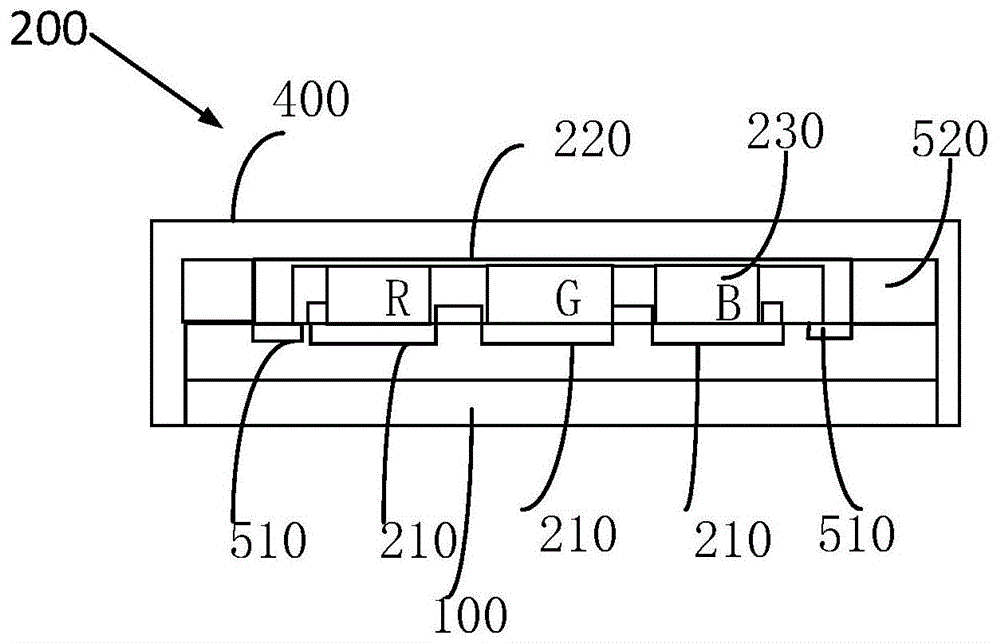
至少部分所述显示像素单元200包括相对设置的第一电极210和第二电极220、及设置于所述第一电极210和所述第二电极220之间的发光层230,所述多条走线包括第一走线310和第二走线320,所述第一电极210之间通过在所述桥140及所述岛130上所布设的所述第一走线310连接,且所述第二电极220之间通过在所述桥140及所述岛130上所布设的所述第二走线320连接。At least part of the
上述方案中,所述衬底基板100为柔性材料,在所述衬底基板100上设置多个独立的岛130和连接在各岛130之间的桥140,走线从岛130之间的桥140上通过,受到外力时,岛130间的距离变大,桥140仍然相连,以保证整个可拉伸显示基板的完整性,其中,第一电极通过设置在岛和桥上的第一走线进行信号传输,本发明实施例的可拉伸显示基板相较于传统的平面显示基板来说,对第二电极220(可作为阴极)搭接部分进行了重新设计,将岛130之间的桥140作为第二电极信号线传输路径,第二电极220不再从屏幕边缘进行搭接,而是在通过桥140上的走线进行连接和信号传输。图2所示为图1中一个岛130的结构放大图,图3所示为图2中A-A向的剖视图,如图2和图3所示,一个独立的岛130上设置有第一走线310(可作为阳极信号线)和第二走线320(可作为阴极信号线),由于整个可拉伸显示基板的第二电极220电位可看作是一致的,因此同一个显示像素单元200的两端均可通过不同的桥140来提供相同的第二电极220电位。这样,可拉伸显示基板进行拉伸动作时,即使第二电极220电阻发生较大变化,但其所对应的走线仍是与第二电极220进行独立连接的,可以保证较好的耐弯性和及远离驱动IC端的电压下降的问题,以提供稳定的电位。In the above solution, the
需要说明的是,在上述方案中,每一所述岛130上至少设置有一所述显示像素单元200,所指的是,如图1所示,每一所述岛130上可对应设置一个所述显示像素单元200,或者,每一所述岛130上也可以对应设置两个或多个所述显示像素单元200;此外,可以是每一所述显示像素单元中的第一电极利用第一走线连接,第二电极利用第二走线连接,也可以是整个显示器件的衬底基板上仅局部一部分显示像素单元中采用上述第一电极利用第一走线连接,第二电极利用第二走线连接的结构。It should be noted that, in the above solution, at least one of the
在本发明所提供的优选实施例中,如图3所示,所述第一走线310、所述第二走线320及所述第一电极210同层且同材料设置。In the preferred embodiment provided by the present invention, as shown in FIG. 3 , the
采用上述方案,可将所述第一走线310、所述第二走线320及所述第一电极210采用同一次构图工艺形成,这样,可以简化制程。当然可以理解的是,在实际应用中,也可以是第一走线310、第二走线320和第一电极210分别位于不同层,对于第一走线310、第二走线320和第一电极210所采用的材料也不进行限定。With the above solution, the
此外,在本发明所提供的优选实施例中,如图3所示,各所述所述可拉伸显示基板还包括:封装层400,每一所述显示像素单元200中的所述第一电极210、所述第二电极220及所述发光层230通过所述封装层400单独封装。In addition, in the preferred embodiment provided by the present invention, as shown in FIG. 3 , each of the stretchable display substrates further includes: an
采用上述方案,如图3所示,每一独立的所述岛130可包含R、G、B三种颜色,同时,每一所述岛130上对应的第一电极210和第二电极220可单独设置,这样,每一所述岛130可单独封装,以确保封装结构防水氧的特性。With the above solution, as shown in FIG. 3 , each
此外,如图3所示,在本发明所提供的优选实施例中,每一所述显示像素单元200还包括:In addition, as shown in FIG. 3, in the preferred embodiment provided by the present invention, each of the
与所述第一电极210同层且同材料设置的搭接电极区510,且所述搭接电极区510与所述第二走线320电连接;an
及,设置于所述搭接电极区510的远离所述衬底基板的一侧的平坦层520,所述平坦层520位于所述发光层的外围,且所述平坦层520在与所述搭接电极区510对应位置设有过孔;And, the
其中,所述第二电极220位于所述第一电极210的远离所述衬底基板100的一侧,且所述第二电极220通过所述平坦层520上的所述过孔与所述搭接电极区510电连接。Wherein, the
采用上述方案,如图3所示,在所述显示像素单元200内部,在所述第一电极210以外、所述封装层400的封装区域以内,还存在着裸露的搭接电极区510,该搭接电极区510与第二走线320电连接,在蒸镀完发光材料后将进行第二电极220的蒸镀,使得第二电极220与裸露的搭接电极区510接触,即完成了整个第二电极220与第二走线320之间的连接回路。With the above solution, as shown in FIG. 3 , inside the
所述搭接电极区510可与所述第一电极210、所述第一走线310和所述第二走线320同层且同材料设置,这样,使得该搭接电极区510也可由所述第一电极210的掩模板进行控制形成,使得在封装区域之外没有第二电极220的材料,所述封装层400能够紧密与周边相结合。The
此外,需要说明的是,平坦层520设置于所述封装层400的封装区域内,并位于发光层230外围,以起到平坦化发光层230的目的,以便于将所述第二电极220制作于发光层230及平坦层520之上。In addition, it should be noted that the
此外,如图2和图3所示,优选的,每个所述岛130上至少设置有两个搭接电极区510,以保证提供稳定的电位。In addition, as shown in FIG. 2 and FIG. 3 , preferably, at least two overlapping
此外,需要说明的是,在本发明所提供的实施例中,在所述第一分割带110和所述第二分割带120可以是镂空结构,即,在所述第一分割带110和所述第二分割带120所在区域为空白区域,也可以是填充有弹性材料,例如:PDMS(Polydimethylsiloxane,聚二甲基硅氧烷)等,这样,不可拉伸的衬底基板100由于在第一分割带110和第二分割带120为镂空结构或者填充可拉伸的弹性材料,可以具备拉伸能力。但是,由于填充弹性材料时,在拉伸时仍有粘附力不佳的可能,因此走线仍需要绕行所述显示像素单元200排布。In addition, it should be noted that, in the embodiment provided by the present invention, the
为保证所述可拉伸显示基板在横、纵方向(如图4中X方向为横向方向,Y为纵向方向,该横、纵方向即分别为所述岛130呈阵列分布的行、列方向,其中,图4中仅示意出了衬底基板的结构,对于所述显示像素单元未进行示意)上均能实现拉伸能力,通常需要将拉伸的第一分割带110和第二分割带120设计为两个方向,例如,第一分割带110横向走向,第二分割带120纵向走向,同时横、纵方向上的第一分割带110和第二分割带120正交设置,并周期性的重复(如图4所示)。这样,为了避让第一分割带110和第二分割带120所在的空白区域或弹性材料填充区域,在横、纵方向上的走线需要绕行所述显示像素单元200排布,才能实现对同一行或同一列上的显示像素单元200进行控制,但是,这种绕行走线会产生较高的压降(IR Drop),不利于显示效果的均匀。如图4所示,虚线表示同一行显示像素单元之间的走线的排列方式示意图,因需要绕行而产生的多余走线,且并不是每个显示像素单元200都需要绕行,导致走线变化也不均匀。In order to ensure the horizontal and vertical directions of the stretchable display substrate (as shown in FIG. 4 , the X direction is the horizontal direction and Y is the vertical direction, and the horizontal and vertical directions are the row and column directions in which the
图5所示为本发明所提供的另一种实施例中的可拉伸显示基板的结构示意图,其中仅示意出了衬底基板,未示意显示像素单元。为了解决上述问题,本发明所提供的优选实施例中,优选的,如图5所示,所述第一分割带110的延伸方向与所述多个岛130的行方向之间具有斜夹角α,所述第二分割带120的延伸方向与所述第一分割带110的延伸方向垂直。FIG. 5 is a schematic structural diagram of a stretchable display substrate in another embodiment provided by the present invention, in which only a base substrate is shown, and a display pixel unit is not shown. In order to solve the above problem, in the preferred embodiment provided by the present invention, preferably, as shown in FIG. 5 , there is an oblique angle between the extending direction of the
采用上述方案,如图5所示,衬底基板上的多个岛130呈阵列分布,其具有行方向和列方向,其中行方向所指的是:由于处于同一行的多个岛130上的显示像素单元200之间可通过同一信号走线(如:栅线)来施加电信号,行方向所指的即是,阵列排布的多个岛中,通过同一信号走线所连接的岛的第一排列方向;列方向所指的是:由于同一列的多个岛130上的显示像素单元200之间可通过同一信号走线(如:数据线)来施加电信号,列方向所指的即是,阵列排布的多个岛中,通过同一信号走线所连接的岛的第二排列方向,行方向与列方向垂直,例如,图5中该行方向为X方向所示,列方向为Y方向所示。上述方案中,可以将分割独立岛130的第一分割带110和第二分割带120的走向进行改进,将第一分割带110设计为其走向与所述多个岛130的行走向之间具有斜夹角α,即,将第一分割带110设计为斜向,第二分割带120与第一分割带110垂直,并且两个方向上的第一分割带110和第二分割带120依然保持周期性排布,这样,可以使得同一行或者同一列的显示像素单元200之间的走线按折线的方式进行排列,如图5所示,同一行的显示像素单元200之间的走线按照图5所示的虚线所示的折线方式进行排列。这样,既保证了单行或单列像素的可控性,又缩短了走线绕行的距离,同时,斜方向且正交的第一分割带110和第二分割带120在配合横、纵方向上的拉伸时,两个斜方向上的组合应变也可以满足横、纵拉伸的要求。With the above solution, as shown in FIG. 5 , the plurality of
优选的,所述斜夹角α为45°。这样,可以使得走线绕行距离最短。并且,每一显示像素单元200的走线绕行方式相同,走线变化均匀。当然可以理解的是,在实际应用中,所述斜夹角α还可以为大于0度小于90度的其他角度。Preferably, the oblique angle α is 45°. In this way, the routing distance of the traces can be minimized. Moreover, the wirings of each
此外,本发明实施例中还提供了一种显示装置,包括本发明实施例所提供的可拉伸显示基板。In addition, an embodiment of the present invention also provides a display device including the stretchable display substrate provided by the embodiment of the present invention.
此外,本发明实施例中还提供了一种可拉伸显示基板的制造方法,所述方法应用于制作本发明实施例所提供的可拉伸显示基板,所述方法包括:In addition, an embodiment of the present invention also provides a manufacturing method of a stretchable display substrate, the method is applied to manufacture the stretchable display substrate provided by the embodiment of the present invention, and the method includes:
提供一衬底基板100,所述衬底基板100上分布有交叉且相互不贯通的多条第一分割带110和多条第二分割带120,所述第一分割带110和所述第二分割带120将所述衬底基板100分割形成为呈阵列分布的多个岛130、及连接所述多个岛130中的每个岛130的多个桥140;A
在所述衬底基板100上形成多个显示像素单元200及电连接所述显示像素单元200的多条走线,其中每一所述岛130至少对应一所述显示像素单元200,每一所述显示像素单元200包括相对设置的第一电极210和第二电极220、及设置于所述第一电极210和所述第二电极220之间的发光层230,所述多条走线包括第一走线310和第二走线320,所述第一电极210之间通过在所述桥140及所述岛130上所布设的所述第一走线310连接,且所述第二电极220之间通过在所述桥140及所述岛130上所布设的所述第二走线320连接。A plurality of
上述方案中,所述衬底基板100为柔性材料,在所述衬底基板100上设置多个独立的岛130和连接在各岛130之间的桥140,走线从岛130之间的桥140上通过,受到外力时,岛130间的距离变大,桥140仍然相连,以保证整个可拉伸显示基板的完整性,其中,本发明实施例的可拉伸显示基板的第二电极220相较于传统的平面显示基板来说,对第二电极220(可作为阴极)搭接部分进行了重新设计,将岛130之间的桥140作为信号线传输的路径,同时,第二电极220不再从屏幕边缘进行搭接,而是在通过桥140上的走线进行连接和信号传输。图2所示为图1中一个岛130的结构放大图,图3所示为图2中A-A向的剖视图,如图2和图3所示,一个独立的岛130上,设置有第一走线310(可作为阳极信号线)和第二走线320(可作为阴极信号线),由于整个可拉伸显示基板的第二电极220电位可看作是一致的,因此同一个显示像素单元200的两端均可通过不同的桥140来提供相同的第二电极220电位。这样,可拉伸显示基板进行拉伸动作时,即使第二电极220电阻发生较大变化,但其所对应的走线仍是与第二电极220进行独立连接的,可以保证较好的耐弯性和及远离驱动IC端的电压下降的问题,以提供稳定的电位。In the above solution, the
进一步的,所述方法中,采用同一次构图工艺形成所述第一走线310、所述第二走线320及所述第一电极210。Further, in the method, the
采用上述方案,可将所述第一走线310、所述第二走线320及所述第一电极210采用同一次构图工艺形成,这样,可以简化制程。当然可以理解的是,在实际应用中,也可以是第一走线310、第二走线320和第一电极210分为位于不同层,可采用不同构图工艺形成,且对于第一走线310、第二走线320和第一电极210所采用的材料也不进行限定。With the above solution, the
进一步的,所述方法还包括:Further, the method also includes:
在所述衬底基板100上形成封装层400,其中每一所述显示像素单元200中的所述第一电极210、所述第二电极220及所述发光层230通过所述封装层400单独封装。An
采用上述方案,如图3所示,每一独立的所述岛130可包含R、G、B三种颜色,同时,每一所述岛130上对应的第一电极210和第二电极220可单独设置,这样,可将每一所述岛130可单独封装,以确保封装结构防水氧的特性。With the above solution, as shown in FIG. 3 , each
进一步的,所述方法中,所述在所述衬底基板100上形成多个显示像素单元200及电连接所述显示像素单元200的多条走线,具体包括:Further, in the method, forming a plurality of
在所述衬底基板100上形成第一电极210和搭接电极区510,所述搭接电极区510与所述第二走线320电连接;forming a
在所述第一电极210上形成所述发光层230,在所述搭接电极区510上、所述发光层的外围形成平坦层520,所述平坦层520在与所述搭接电极区510对应位置设有过孔;The
在所述发光层230及所述平坦层520上形成第二电极220,所述第二电极220通过所述平坦层520上的所述过孔与所述搭接电极区510电连接。A
采用上述方案,如图3所示,在所述显示像素单元200内部,在所述第一电极210以外、所述封装层400的封装区域以内,还存在着裸露的搭接电极区510,该搭接电极区510与第二走线320电连接,在蒸镀完发光材料后将进行第二电极220的蒸镀,使得第二电极220与裸露的搭接电极区510接触,即完成了整个第二电极220与第二走线320之间的连接回路。With the above solution, as shown in FIG. 3 , inside the
所述搭接电极区510可与所述第一电极210、所述第一走线310和所述第二走线320同层且同材料设置,这样,使得该搭接电极区510也可由所述第一电极210的掩模板进行控制,使得在封装区域之外没有第二电极220的材料,所述封装层400能够紧密与周边相结合。The
此外,如图3所示,优选的,每个所述岛130上至少设置有两个搭接电极区510,以保证提供稳定的电位。In addition, as shown in FIG. 3 , preferably, each of the
以上所述仅是本发明的优选实施方式,应当指出,对于本技术领域的普通技术人员来说,在不脱离本发明技术原理的前提下,还可以做出若干改进和替换,这些改进和替换也应视为本发明的保护范围。The above are only the preferred embodiments of the present invention. It should be pointed out that for those skilled in the art, without departing from the technical principle of the present invention, several improvements and replacements can be made. These improvements and replacements It should also be regarded as the protection scope of the present invention.
Claims (12)
Priority Applications (2)
| Application Number | Priority Date | Filing Date | Title |
|---|---|---|---|
| CN201811148865.7A CN109308851B (en) | 2018-09-29 | 2018-09-29 | Stretchable display substrate, method for manufacturing the same, and display device |
| US16/585,443 US10902755B2 (en) | 2018-09-29 | 2019-09-27 | Stretchable display substrate, method for manufacturing stretchable display substrate, and display device |
Applications Claiming Priority (1)
| Application Number | Priority Date | Filing Date | Title |
|---|---|---|---|
| CN201811148865.7A CN109308851B (en) | 2018-09-29 | 2018-09-29 | Stretchable display substrate, method for manufacturing the same, and display device |
Publications (2)
| Publication Number | Publication Date |
|---|---|
| CN109308851A CN109308851A (en) | 2019-02-05 |
| CN109308851B true CN109308851B (en) | 2020-12-22 |
Family
ID=65225291
Family Applications (1)
| Application Number | Title | Priority Date | Filing Date |
|---|---|---|---|
| CN201811148865.7A Active CN109308851B (en) | 2018-09-29 | 2018-09-29 | Stretchable display substrate, method for manufacturing the same, and display device |
Country Status (2)
| Country | Link |
|---|---|
| US (1) | US10902755B2 (en) |
| CN (1) | CN109308851B (en) |
Families Citing this family (28)
| Publication number | Priority date | Publication date | Assignee | Title |
|---|---|---|---|---|
| DE112019005974T5 (en) * | 2018-11-30 | 2021-09-09 | Sony Group Corporation | DISPLAY DEVICE |
| CN109830614B (en) | 2019-02-19 | 2020-11-13 | 京东方科技集团股份有限公司 | Flexible display substrate and flexible display device |
| CN111627325B (en) * | 2019-02-27 | 2022-05-13 | 昆山工研院新型平板显示技术中心有限公司 | Display panel mother board, display panel and preparation method of display panel |
| CN109920803B (en) | 2019-03-25 | 2020-12-11 | 京东方科技集团股份有限公司 | A stretchable display substrate and display device |
| CN109920334B (en) * | 2019-03-27 | 2021-04-27 | 京东方科技集团股份有限公司 | Array substrate and display device |
| CN110350014B (en) | 2019-07-17 | 2021-10-26 | 京东方科技集团股份有限公司 | Display substrate, display device and preparation method of display substrate |
| CN110428740B (en) * | 2019-08-07 | 2021-04-30 | 京东方科技集团股份有限公司 | Pixel unit, display panel and display device |
| CN110599908B (en) * | 2019-09-20 | 2021-06-29 | 云谷(固安)科技有限公司 | Display panel, method for producing the same, and display device |
| CN110649181B (en) * | 2019-10-08 | 2022-04-26 | 京东方科技集团股份有限公司 | Display substrate, display device and preparation method of display substrate |
| KR102826594B1 (en) * | 2019-10-24 | 2025-06-27 | 엘지디스플레이 주식회사 | Stretchable display device |
| CN110854166A (en) * | 2019-10-28 | 2020-02-28 | 武汉华星光电半导体显示技术有限公司 | Stretchable organic light-emitting diode display panel |
| CN110634937B (en) * | 2019-10-31 | 2022-04-26 | 京东方科技集团股份有限公司 | Display substrate, preparation method thereof and display device |
| CN111210726B (en) | 2020-02-26 | 2022-07-15 | 京东方科技集团股份有限公司 | Stretchable display panel and stretchable display device |
| CN113629103A (en) * | 2020-05-08 | 2021-11-09 | 深圳市柔宇科技有限公司 | Flexible display panel |
| CN111682049B (en) * | 2020-06-19 | 2023-08-22 | 京东方科技集团股份有限公司 | Display substrate, display device and mask |
| CN113838371B (en) * | 2020-08-21 | 2022-12-27 | 友达光电股份有限公司 | Stretchable pixel array substrate |
| CN113870695B (en) * | 2020-08-21 | 2024-01-26 | 友达光电股份有限公司 | stretchable display |
| CN111883544B (en) * | 2020-08-25 | 2024-07-02 | 京东方科技集团股份有限公司 | Display panel, display device, electronic device and manufacturing method |
| CN112310323A (en) * | 2020-10-30 | 2021-02-02 | 京东方科技集团股份有限公司 | A display panel, method of making the same, and display device |
| CN112510070B (en) * | 2020-11-30 | 2024-03-12 | 京东方科技集团股份有限公司 | Stretchable array substrate, stretchable display panel and production method |
| CN112582382B (en) * | 2020-12-07 | 2023-05-09 | 天马微电子股份有限公司 | Display panel and display device |
| CN114842745B (en) * | 2022-04-02 | 2023-10-13 | Tcl华星光电技术有限公司 | Display assembly and display device |
| CN115274790B (en) * | 2022-07-20 | 2024-08-09 | 武汉华星光电半导体显示技术有限公司 | Display panel and manufacturing method thereof |
| CN116125722A (en) * | 2022-12-22 | 2023-05-16 | 惠科股份有限公司 | Electronic paper display screen and display device |
| WO2024150388A1 (en) * | 2023-01-13 | 2024-07-18 | シャープディスプレイテクノロジー株式会社 | Stretchable display device |
| CN116416878B (en) * | 2023-03-22 | 2023-09-26 | 大连理工大学 | Flexible LED lattice screen without image distortion under large stretching quantity |
| CN117560954B (en) * | 2023-12-19 | 2024-09-06 | 惠科股份有限公司 | Display panel and display device |
| CN117794321B (en) * | 2023-12-27 | 2024-11-22 | 惠科股份有限公司 | Display panel and display device |
Family Cites Families (11)
| Publication number | Priority date | Publication date | Assignee | Title |
|---|---|---|---|---|
| KR101032337B1 (en) * | 2002-12-13 | 2011-05-09 | 가부시키가이샤 한도오따이 에네루기 켄큐쇼 | Light emitting device and manufacturing method thereof |
| CN202018547U (en) * | 2011-04-15 | 2011-10-26 | Tcl显示科技(惠州)有限公司 | Main flexible printed circuit for liquid crystal display module |
| US9730330B1 (en) * | 2013-11-21 | 2017-08-08 | H4 Engineering, Inc. | Compliant electronic devices |
| KR102282492B1 (en) * | 2015-03-10 | 2021-07-27 | 삼성디스플레이 주식회사 | Organic light emitting diode display |
| KR102271598B1 (en) * | 2015-04-01 | 2021-07-02 | 삼성디스플레이 주식회사 | Stretchable device |
| KR101973163B1 (en) * | 2016-03-22 | 2019-04-29 | 삼성디스플레이 주식회사 | Display device |
| KR102524535B1 (en) * | 2016-03-29 | 2023-04-24 | 삼성디스플레이 주식회사 | Display device |
| CN107633807B (en) * | 2017-09-08 | 2019-10-15 | 上海天马有机发光显示技术有限公司 | A display panel and display device |
| CN108054173B (en) * | 2017-12-13 | 2021-01-26 | 京东方科技集团股份有限公司 | Display substrate, preparation method and display device |
| KR102498621B1 (en) * | 2017-12-29 | 2023-02-10 | 삼성디스플레이 주식회사 | Flexible Display Device |
| CN108598125B (en) * | 2018-05-07 | 2019-09-13 | 京东方科技集团股份有限公司 | Flexible display panel, flexible display device and method for manufacturing flexible display panel |
-
2018
- 2018-09-29 CN CN201811148865.7A patent/CN109308851B/en active Active
-
2019
- 2019-09-27 US US16/585,443 patent/US10902755B2/en active Active
Also Published As
| Publication number | Publication date |
|---|---|
| US10902755B2 (en) | 2021-01-26 |
| CN109308851A (en) | 2019-02-05 |
| US20200105170A1 (en) | 2020-04-02 |
Similar Documents
| Publication | Publication Date | Title |
|---|---|---|
| CN109308851B (en) | Stretchable display substrate, method for manufacturing the same, and display device | |
| KR102658459B1 (en) | Display device | |
| JP7415245B2 (en) | Device including pixel island, manufacturing method of device including pixel island, and display device | |
| CN112863342B (en) | Stretchable display module and stretchable display equipment | |
| KR101810304B1 (en) | Flexible display | |
| US10249697B2 (en) | Display panel and display device | |
| KR102886543B1 (en) | Transparent display panel and transparent display device including the same | |
| US6700636B2 (en) | Liquid crystal display panel and method for manufacturing the same | |
| CN111341813B (en) | Display panel and display device | |
| TWI461806B (en) | Lead line strcuture and display panel having the same | |
| CN113767475A (en) | Flexible display panel, display device and manufacturing method | |
| CN111403420B (en) | Pixel array substrate and driving method thereof | |
| CN119277817A (en) | Display panel and display device | |
| WO2022151528A1 (en) | Stretchable display module | |
| WO2020181634A1 (en) | Oled display device and manufacturing method therefor | |
| KR102582066B1 (en) | Chip on film package and display device including the chip on film package | |
| WO2020155287A1 (en) | Display panel and display device | |
| CN108598290A (en) | Flexible display and preparation method thereof | |
| US20220391042A1 (en) | Display panel and display apparatus | |
| KR20120050147A (en) | Thin film transistor array panel | |
| CN112991942B (en) | Stretchable display substrate and display device | |
| WO2020014933A1 (en) | Flexible display panel, manufacturing method therefor, display device, and mask | |
| JP2002148654A (en) | Liquid crystal display | |
| US20200117312A1 (en) | Touch screen including an inspection line and a display device having the same | |
| CN113157142B (en) | Touch display panel and display device |
Legal Events
| Date | Code | Title | Description |
|---|---|---|---|
| PB01 | Publication | ||
| PB01 | Publication | ||
| SE01 | Entry into force of request for substantive examination | ||
| SE01 | Entry into force of request for substantive examination | ||
| GR01 | Patent grant | ||
| GR01 | Patent grant |