CN109285504B - Shifting register unit, driving method thereof and grid driving circuit - Google Patents
Shifting register unit, driving method thereof and grid driving circuit Download PDFInfo
- Publication number
- CN109285504B CN109285504B CN201710594509.7A CN201710594509A CN109285504B CN 109285504 B CN109285504 B CN 109285504B CN 201710594509 A CN201710594509 A CN 201710594509A CN 109285504 B CN109285504 B CN 109285504B
- Authority
- CN
- China
- Prior art keywords
- transistor
- coupled
- voltage
- pull
- control
- Prior art date
- Legal status (The legal status is an assumption and is not a legal conclusion. Google has not performed a legal analysis and makes no representation as to the accuracy of the status listed.)
- Active
Links
Images


Classifications
-
- G—PHYSICS
- G09—EDUCATION; CRYPTOGRAPHY; DISPLAY; ADVERTISING; SEALS
- G09G—ARRANGEMENTS OR CIRCUITS FOR CONTROL OF INDICATING DEVICES USING STATIC MEANS TO PRESENT VARIABLE INFORMATION
- G09G3/00—Control arrangements or circuits, of interest only in connection with visual indicators other than cathode-ray tubes
- G09G3/20—Control arrangements or circuits, of interest only in connection with visual indicators other than cathode-ray tubes for presentation of an assembly of a number of characters, e.g. a page, by composing the assembly by combination of individual elements arranged in a matrix no fixed position being assigned to or needed to be assigned to the individual characters or partial characters
- G09G3/22—Control arrangements or circuits, of interest only in connection with visual indicators other than cathode-ray tubes for presentation of an assembly of a number of characters, e.g. a page, by composing the assembly by combination of individual elements arranged in a matrix no fixed position being assigned to or needed to be assigned to the individual characters or partial characters using controlled light sources
- G09G3/30—Control arrangements or circuits, of interest only in connection with visual indicators other than cathode-ray tubes for presentation of an assembly of a number of characters, e.g. a page, by composing the assembly by combination of individual elements arranged in a matrix no fixed position being assigned to or needed to be assigned to the individual characters or partial characters using controlled light sources using electroluminescent panels
- G09G3/32—Control arrangements or circuits, of interest only in connection with visual indicators other than cathode-ray tubes for presentation of an assembly of a number of characters, e.g. a page, by composing the assembly by combination of individual elements arranged in a matrix no fixed position being assigned to or needed to be assigned to the individual characters or partial characters using controlled light sources using electroluminescent panels semiconductive, e.g. using light-emitting diodes [LED]
- G09G3/3208—Control arrangements or circuits, of interest only in connection with visual indicators other than cathode-ray tubes for presentation of an assembly of a number of characters, e.g. a page, by composing the assembly by combination of individual elements arranged in a matrix no fixed position being assigned to or needed to be assigned to the individual characters or partial characters using controlled light sources using electroluminescent panels semiconductive, e.g. using light-emitting diodes [LED] organic, e.g. using organic light-emitting diodes [OLED]
- G09G3/3266—Details of drivers for scan electrodes
-
- G—PHYSICS
- G09—EDUCATION; CRYPTOGRAPHY; DISPLAY; ADVERTISING; SEALS
- G09G—ARRANGEMENTS OR CIRCUITS FOR CONTROL OF INDICATING DEVICES USING STATIC MEANS TO PRESENT VARIABLE INFORMATION
- G09G3/00—Control arrangements or circuits, of interest only in connection with visual indicators other than cathode-ray tubes
- G09G3/20—Control arrangements or circuits, of interest only in connection with visual indicators other than cathode-ray tubes for presentation of an assembly of a number of characters, e.g. a page, by composing the assembly by combination of individual elements arranged in a matrix no fixed position being assigned to or needed to be assigned to the individual characters or partial characters
- G09G3/34—Control arrangements or circuits, of interest only in connection with visual indicators other than cathode-ray tubes for presentation of an assembly of a number of characters, e.g. a page, by composing the assembly by combination of individual elements arranged in a matrix no fixed position being assigned to or needed to be assigned to the individual characters or partial characters by control of light from an independent source
- G09G3/36—Control arrangements or circuits, of interest only in connection with visual indicators other than cathode-ray tubes for presentation of an assembly of a number of characters, e.g. a page, by composing the assembly by combination of individual elements arranged in a matrix no fixed position being assigned to or needed to be assigned to the individual characters or partial characters by control of light from an independent source using liquid crystals
- G09G3/3611—Control of matrices with row and column drivers
- G09G3/3674—Details of drivers for scan electrodes
- G09G3/3677—Details of drivers for scan electrodes suitable for active matrices only
-
- G—PHYSICS
- G09—EDUCATION; CRYPTOGRAPHY; DISPLAY; ADVERTISING; SEALS
- G09G—ARRANGEMENTS OR CIRCUITS FOR CONTROL OF INDICATING DEVICES USING STATIC MEANS TO PRESENT VARIABLE INFORMATION
- G09G3/00—Control arrangements or circuits, of interest only in connection with visual indicators other than cathode-ray tubes
- G09G3/20—Control arrangements or circuits, of interest only in connection with visual indicators other than cathode-ray tubes for presentation of an assembly of a number of characters, e.g. a page, by composing the assembly by combination of individual elements arranged in a matrix no fixed position being assigned to or needed to be assigned to the individual characters or partial characters
- G09G3/2092—Details of a display terminals using a flat panel, the details relating to the control arrangement of the display terminal and to the interfaces thereto
-
- G—PHYSICS
- G09—EDUCATION; CRYPTOGRAPHY; DISPLAY; ADVERTISING; SEALS
- G09G—ARRANGEMENTS OR CIRCUITS FOR CONTROL OF INDICATING DEVICES USING STATIC MEANS TO PRESENT VARIABLE INFORMATION
- G09G3/00—Control arrangements or circuits, of interest only in connection with visual indicators other than cathode-ray tubes
- G09G3/20—Control arrangements or circuits, of interest only in connection with visual indicators other than cathode-ray tubes for presentation of an assembly of a number of characters, e.g. a page, by composing the assembly by combination of individual elements arranged in a matrix no fixed position being assigned to or needed to be assigned to the individual characters or partial characters
- G09G3/22—Control arrangements or circuits, of interest only in connection with visual indicators other than cathode-ray tubes for presentation of an assembly of a number of characters, e.g. a page, by composing the assembly by combination of individual elements arranged in a matrix no fixed position being assigned to or needed to be assigned to the individual characters or partial characters using controlled light sources
- G09G3/30—Control arrangements or circuits, of interest only in connection with visual indicators other than cathode-ray tubes for presentation of an assembly of a number of characters, e.g. a page, by composing the assembly by combination of individual elements arranged in a matrix no fixed position being assigned to or needed to be assigned to the individual characters or partial characters using controlled light sources using electroluminescent panels
- G09G3/32—Control arrangements or circuits, of interest only in connection with visual indicators other than cathode-ray tubes for presentation of an assembly of a number of characters, e.g. a page, by composing the assembly by combination of individual elements arranged in a matrix no fixed position being assigned to or needed to be assigned to the individual characters or partial characters using controlled light sources using electroluminescent panels semiconductive, e.g. using light-emitting diodes [LED]
- G09G3/3208—Control arrangements or circuits, of interest only in connection with visual indicators other than cathode-ray tubes for presentation of an assembly of a number of characters, e.g. a page, by composing the assembly by combination of individual elements arranged in a matrix no fixed position being assigned to or needed to be assigned to the individual characters or partial characters using controlled light sources using electroluminescent panels semiconductive, e.g. using light-emitting diodes [LED] organic, e.g. using organic light-emitting diodes [OLED]
- G09G3/3225—Control arrangements or circuits, of interest only in connection with visual indicators other than cathode-ray tubes for presentation of an assembly of a number of characters, e.g. a page, by composing the assembly by combination of individual elements arranged in a matrix no fixed position being assigned to or needed to be assigned to the individual characters or partial characters using controlled light sources using electroluminescent panels semiconductive, e.g. using light-emitting diodes [LED] organic, e.g. using organic light-emitting diodes [OLED] using an active matrix
- G09G3/3258—Control arrangements or circuits, of interest only in connection with visual indicators other than cathode-ray tubes for presentation of an assembly of a number of characters, e.g. a page, by composing the assembly by combination of individual elements arranged in a matrix no fixed position being assigned to or needed to be assigned to the individual characters or partial characters using controlled light sources using electroluminescent panels semiconductive, e.g. using light-emitting diodes [LED] organic, e.g. using organic light-emitting diodes [OLED] using an active matrix with pixel circuitry controlling the voltage across the light-emitting element
-
- G—PHYSICS
- G11—INFORMATION STORAGE
- G11C—STATIC STORES
- G11C19/00—Digital stores in which the information is moved stepwise, e.g. shift registers
- G11C19/28—Digital stores in which the information is moved stepwise, e.g. shift registers using semiconductor elements
-
- G—PHYSICS
- G09—EDUCATION; CRYPTOGRAPHY; DISPLAY; ADVERTISING; SEALS
- G09G—ARRANGEMENTS OR CIRCUITS FOR CONTROL OF INDICATING DEVICES USING STATIC MEANS TO PRESENT VARIABLE INFORMATION
- G09G2300/00—Aspects of the constitution of display devices
- G09G2300/04—Structural and physical details of display devices
- G09G2300/0421—Structural details of the set of electrodes
- G09G2300/0426—Layout of electrodes and connections
-
- G—PHYSICS
- G09—EDUCATION; CRYPTOGRAPHY; DISPLAY; ADVERTISING; SEALS
- G09G—ARRANGEMENTS OR CIRCUITS FOR CONTROL OF INDICATING DEVICES USING STATIC MEANS TO PRESENT VARIABLE INFORMATION
- G09G2310/00—Command of the display device
- G09G2310/02—Addressing, scanning or driving the display screen or processing steps related thereto
- G09G2310/0264—Details of driving circuits
- G09G2310/0267—Details of drivers for scan electrodes, other than drivers for liquid crystal, plasma or OLED displays
-
- G—PHYSICS
- G09—EDUCATION; CRYPTOGRAPHY; DISPLAY; ADVERTISING; SEALS
- G09G—ARRANGEMENTS OR CIRCUITS FOR CONTROL OF INDICATING DEVICES USING STATIC MEANS TO PRESENT VARIABLE INFORMATION
- G09G2310/00—Command of the display device
- G09G2310/02—Addressing, scanning or driving the display screen or processing steps related thereto
- G09G2310/0264—Details of driving circuits
- G09G2310/0286—Details of a shift registers arranged for use in a driving circuit
-
- G—PHYSICS
- G09—EDUCATION; CRYPTOGRAPHY; DISPLAY; ADVERTISING; SEALS
- G09G—ARRANGEMENTS OR CIRCUITS FOR CONTROL OF INDICATING DEVICES USING STATIC MEANS TO PRESENT VARIABLE INFORMATION
- G09G2310/00—Command of the display device
- G09G2310/08—Details of timing specific for flat panels, other than clock recovery
Landscapes
- Engineering & Computer Science (AREA)
- Physics & Mathematics (AREA)
- Computer Hardware Design (AREA)
- General Physics & Mathematics (AREA)
- Theoretical Computer Science (AREA)
- Chemical & Material Sciences (AREA)
- Crystallography & Structural Chemistry (AREA)
- Control Of Indicators Other Than Cathode Ray Tubes (AREA)
- Shift Register Type Memory (AREA)
- Control Of El Displays (AREA)
Abstract
本发明的实施例发明了移位寄存器单元及其驱动方法、栅极驱动电路。移位寄存器单元包括输入模块、下级启动模块、控制模块、稳定模块、至少一个输出模块。至少一个输出模块被配置为根据上拉节点的电压、下拉节点的电压、第一电压信号、来自各自的控制时钟信号端的控制时钟信号、以及来自各自的控制电压信号端的控制电压信号,控制各自的信号输出端的电压。在第一时钟信号的高电平结束时,第二时钟信号的高电平开始,在第二时钟信号的高电平结束时,第三时钟信号的高电平开始。
The embodiment of the present invention invents a shift register unit, a driving method thereof, and a gate driving circuit. The shift register unit includes an input module, a lower-level startup module, a control module, a stabilization module, and at least one output module. The at least one output module is configured to control the respective control voltage signals according to the voltage of the pull-up node, the voltage of the pull-down node, the first voltage signal, the control clock signal from the respective control clock signal terminal, and the control voltage signal from the respective control voltage signal terminal. Voltage at the signal output. When the high level of the first clock signal ends, the high level of the second clock signal begins, and when the high level of the second clock signal ends, the high level of the third clock signal begins.
Description
技术领域technical field
本发明涉及显示技术领域,具体地,涉及移位寄存器单元及其驱动方法、栅极驱动电路、阵列基板以及显示装置。The present invention relates to the field of display technology, and in particular, to a shift register unit and a driving method thereof, a gate driving circuit, an array substrate and a display device.
背景技术Background technique
随着显示技术的进步,相对于传统的液晶显示(Liquid Crystal Display,LCD)装置,新一代的有机发光二极管(Organic Light Emitting Diode,OLED)显示装置具有更低的制造成本,更快的反应速度,更高的对比度,更广的视角,更大的工作温度范围,不需要背光单元,色彩鲜艳及轻薄等优点,因此OLED显示技术成为当前发展最快的显示技术。With the advancement of display technology, compared with traditional liquid crystal display (LCD) devices, the new generation of organic light emitting diode (Organic Light Emitting Diode, OLED) display devices has lower manufacturing cost and faster response speed , higher contrast ratio, wider viewing angle, wider operating temperature range, no need for a backlight unit, bright colors and thinness, etc., so OLED display technology has become the fastest growing display technology.
为了提高OLED面板的工艺集成度并降低成本,通常采用阵列基板行驱动(GateDriver on Array,简称GOA)技术而将薄膜晶体管(TFT)的栅极开关电路集成在显示面板的阵列基板上以形成对显示面板的扫描驱动。这种利用GOA技术而集成在阵列基板上的栅极驱动电路也称为GOA电路或移位寄存器电路。采用GOA电路的显示装置由于省去了绑定驱动电路的部分,可以从材料成本和制作工艺两方面降低成本。In order to improve the process integration of the OLED panel and reduce the cost, the gate switch circuit of the thin film transistor (TFT) is usually integrated on the array substrate of the display panel by adopting the gate driver on array (GOA) technology to form a pair of Scan driver for the display panel. The gate driving circuit integrated on the array substrate using the GOA technology is also called a GOA circuit or a shift register circuit. The display device using the GOA circuit can reduce the cost in terms of material cost and manufacturing process because the part of binding the driving circuit is omitted.
发明内容SUMMARY OF THE INVENTION
本发明的实施例提供了一种移位寄存器单元及其驱动方法、栅极驱动电路、基板以及显示装置,其中移位寄存器单元能够在一个触发信号的控制下,输出至少一级栅极驱动信号,并且降低信号噪声、降低功耗、减少漏电流。Embodiments of the present invention provide a shift register unit and a driving method thereof, a gate driving circuit, a substrate and a display device, wherein the shift register unit can output at least one stage of gate driving signals under the control of a trigger signal , and reduce signal noise, reduce power consumption, and reduce leakage current.
根据本发明的一个方面,提供了一种移位寄存器单元,包括:输入模块,其被配置为根据来自第一时钟信号端的第一时钟信号和来自触发信号端的触发信号,控制上拉节点的电压;下级启动模块,其被配置为根据上拉节点的电压、下拉节点的电压、来自第二时钟信号端的第二时钟信号、以及来自第一电压信号端的第一电压信号,控制下级启动信号输出端的电压;控制模块,其被配置为根据上拉节点的电压和来自第二电压信号端的第二电压信号控制下拉节点的电压,以及根据下拉节点的电压和第二电压信号控制上拉节点的电压;稳定模块,其被配置为根据来自第三时钟信号端的第三时钟信号、第一电压信号、以及来自第三电压信号端的第三电压信号,控制上拉节点的电压和下拉节点的电压;以及至少一个输出模块,其被配置为根据上拉节点的电压、下拉节点的电压、第一电压信号、来自各自的控制时钟信号端的控制时钟信号、以及来自各自的控制电压信号端的控制电压信号,控制各自的信号输出端的电压。在第一时钟信号的高电平结束时,第二时钟信号的高电平开始,在第二时钟信号的高电平结束时,第三时钟信号的高电平开始。According to an aspect of the present invention, a shift register unit is provided, comprising: an input module configured to control the voltage of a pull-up node according to a first clock signal from a first clock signal terminal and a trigger signal from a trigger signal terminal a lower-level startup module configured to control the output of the lower-level startup signal according to the voltage of the pull-up node, the voltage of the pull-down node, the second clock signal from the second clock signal terminal, and the first voltage signal from the first voltage signal terminal a voltage; a control module configured to control the voltage of the pull-down node according to the voltage of the pull-up node and the second voltage signal from the second voltage signal terminal, and to control the voltage of the pull-up node according to the voltage of the pull-down node and the second voltage signal; a stabilization module configured to control the voltage of the pull-up node and the voltage of the pull-down node according to the third clock signal from the third clock signal terminal, the first voltage signal, and the third voltage signal from the third voltage signal terminal; and at least an output module configured to control the respective voltage at the signal output. When the high level of the first clock signal ends, the high level of the second clock signal begins, and when the high level of the second clock signal ends, the high level of the third clock signal begins.
在本发明的实施例中,至少一个输出模块中的每个输出模块包括上拉晶体管、下拉晶体管和控制晶体管。上拉晶体管的控制极与上拉节点耦接,其第一极与控制电压信号端耦接,其第二极与信号输出端耦接。下拉晶体管的控制极与下拉节点耦接,其第一极与第一电压信号端耦接,其第二极与信号输出端耦接。控制晶体管的控制极与控制时钟信号端耦接,其第一极与第一电压信号端耦接,其第二极与信号输出端耦接。In an embodiment of the present invention, each of the at least one output module includes a pull-up transistor, a pull-down transistor, and a control transistor. The control electrode of the pull-up transistor is coupled to the pull-up node, the first electrode of the pull-up transistor is coupled to the control voltage signal end, and the second electrode of the pull-up transistor is coupled to the signal output end. The control electrode of the pull-down transistor is coupled to the pull-down node, the first electrode of the pull-down transistor is coupled to the first voltage signal end, and the second electrode of the pull-down transistor is coupled to the signal output end. The control electrode of the control transistor is coupled to the control clock signal end, the first electrode of the control transistor is coupled to the first voltage signal end, and the second electrode of the control transistor is coupled to the signal output end.
在本发明的实施例中,至少一个输出模块包括:第一输出模块,其被配置为根据上拉节点的电压、下拉节点的电压、第一电压信号、来自第一控制时钟信号端的第一控制时钟信号、以及来自第一控制电压信号端的第一控制电压信号,控制第一信号输出端的电压;以及第二输出模块,其被配置为根据上拉节点的电压、下拉节点的电压、第一电压信号、来自第二控制时钟信号端的第二控制时钟信号、以及来自第二控制电压信号端的第二控制电压信号,控制第二信号输出端的电压。In an embodiment of the present invention, at least one output module includes: a first output module configured to control the voltage according to the voltage of the pull-up node, the voltage of the pull-down node, the first voltage signal, and the first control signal from the first control clock signal terminal a clock signal and a first control voltage signal from the first control voltage signal terminal to control the voltage of the first signal output terminal; and a second output module configured to be based on the voltage of the pull-up node, the voltage of the pull-down node, the first voltage The signal, the second control clock signal from the second control clock signal terminal, and the second control voltage signal from the second control voltage signal terminal, control the voltage of the second signal output terminal.
在本发明的实施例中,输入模块包括第一晶体管、第二晶体管和第十二晶体管。第一晶体管的控制极与第一时钟信号端耦接,其第一极与触发信号端耦接,其第二极与第二晶体管的第一极耦接。第二晶体管的控制极与第一时钟信号端耦接,其第一极与第一晶体管的第二极耦接,其第二极与上拉节点耦接。第十二晶体管的控制极与上拉节点耦接,其第一极与第二晶体管的第一极耦接,其第二极与第二时钟信号端耦接。In an embodiment of the present invention, the input module includes a first transistor, a second transistor and a twelfth transistor. The control electrode of the first transistor is coupled with the first clock signal end, the first electrode is coupled with the trigger signal end, and the second electrode is coupled with the first electrode of the second transistor. The control electrode of the second transistor is coupled to the first clock signal terminal, the first electrode of the second transistor is coupled to the second electrode of the first transistor, and the second electrode is coupled to the pull-up node. The control electrode of the twelfth transistor is coupled to the pull-up node, the first electrode of the twelfth transistor is coupled to the first electrode of the second transistor, and the second electrode is coupled to the second clock signal terminal.
在本发明的实施例中,下级启动模块包括第四晶体管、第五晶体管和第一电容器。第四晶体管的控制极与上拉节点耦接,其第一极与第二时钟信号端耦接,其第二极与下级启动信号输出端耦接。第五晶体管的控制极与下拉节点耦接,其第一极与第一电压信号端耦接,其第二极与下级启动信号输出端耦接。第一电容器被耦接在上拉节点和下级启动信号输出端之间。In an embodiment of the present invention, the lower-level startup module includes a fourth transistor, a fifth transistor, and a first capacitor. The control electrode of the fourth transistor is coupled to the pull-up node, the first electrode of the fourth transistor is coupled to the second clock signal end, and the second electrode of the fourth transistor is coupled to the lower-level enable signal output end. The control electrode of the fifth transistor is coupled to the pull-down node, the first electrode of the fifth transistor is coupled to the first voltage signal end, and the second electrode of the fifth transistor is coupled to the lower-level enable signal output end. The first capacitor is coupled between the pull-up node and the lower-level enable signal output terminal.
在本发明的实施例中,控制模块包括第三晶体管和第十五晶体管。第三晶体管的控制极与下拉节点耦接,其第一极与第二电压信号端耦接,其第二极与上拉节点耦接。第十五晶体管的控制极与上拉节点耦接,其第一极与第二电压信号端耦接,其第二极与下拉节点耦接。In an embodiment of the present invention, the control module includes a third transistor and a fifteenth transistor. The control electrode of the third transistor is coupled to the pull-down node, the first electrode of the third transistor is coupled to the second voltage signal end, and the second electrode of the third transistor is coupled to the pull-up node. The control electrode of the fifteenth transistor is coupled to the pull-up node, the first electrode is coupled to the second voltage signal end, and the second electrode is coupled to the pull-down node.
在本发明的实施例中,稳定模块包括第十三晶体管和第十四晶体管。第十三晶体管的控制极与第三时钟信号端耦接,其第一极与第一电压信号端耦接,其第二极与上拉节点耦接。第十四晶体管的控制极与第三时钟信号端耦接,其第一极与第三电压信号端耦接,其第二极与下拉节点耦接。In an embodiment of the present invention, the stabilization module includes a thirteenth transistor and a fourteenth transistor. The control electrode of the thirteenth transistor is coupled to the third clock signal end, the first electrode is coupled to the first voltage signal end, and the second electrode is coupled to the pull-up node. The control electrode of the fourteenth transistor is coupled to the third clock signal end, the first electrode of the transistor is coupled to the third voltage signal end, and the second electrode of the fourteenth transistor is coupled to the pull-down node.
在本发明的实施例中,第一输出模块包括第六晶体管、第七晶体管和第八晶体管。第六晶体管的控制极与上拉节点耦接,其第一极与第一控制电压信号端耦接,其第二极与第一信号输出端耦接;第七晶体管的控制极与下拉节点耦接,其第一极与第一电压信号端耦接,其第二极与第一信号输出端耦接;第八晶体管的控制极与第一控制时钟信号端耦接,其第一极与第一电压信号端耦接,其第二极与第一信号输出端耦接。In an embodiment of the present invention, the first output module includes a sixth transistor, a seventh transistor and an eighth transistor. The control electrode of the sixth transistor is coupled to the pull-up node, the first electrode is coupled to the first control voltage signal terminal, and the second electrode is coupled to the first signal output end; the control electrode of the seventh transistor is coupled to the pull-down node The first pole is coupled with the first voltage signal terminal, the second pole is coupled with the first signal output terminal; the control pole of the eighth transistor is coupled with the first control clock signal terminal, and the first pole is connected with the first signal output terminal. A voltage signal terminal is coupled to the second pole, and the second pole is coupled to the first signal output terminal.
在本发明的实施例中,第七晶体管的宽长比是第六晶体管的宽长比的整数倍。In the embodiment of the present invention, the aspect ratio of the seventh transistor is an integer multiple of the aspect ratio of the sixth transistor.
在本发明的实施例中,第二输出模块包括第九晶体管、第十晶体管和第十一晶体管。第九晶体管的控制极与上拉节点耦接,其第一极与第二控制电压信号端耦接,其第二极与第二信号输出端耦接;第十晶体管的控制极与下拉节点耦接,其第一极与第一电压信号端耦接,其第二极与第二信号输出端耦接;第十一晶体管的控制极与第二控制时钟信号信号端耦接,其第一极与第一电压信号端耦接,其第二极与第二信号输出端耦接。In an embodiment of the present invention, the second output module includes a ninth transistor, a tenth transistor and an eleventh transistor. The control electrode of the ninth transistor is coupled to the pull-up node, the first electrode is coupled to the second control voltage signal terminal, and the second electrode is coupled to the second signal output end; the control electrode of the tenth transistor is coupled to the pull-down node connected, its first pole is coupled to the first voltage signal terminal, its second pole is coupled to the second signal output terminal; the control pole of the eleventh transistor is coupled to the second control clock signal terminal, its first pole It is coupled to the first voltage signal terminal, and the second pole is coupled to the second signal output terminal.
在本发明的实施例中,第十晶体管的宽长比是第九晶体管的宽长比的整数倍。In the embodiment of the present invention, the aspect ratio of the tenth transistor is an integer multiple of the aspect ratio of the ninth transistor.
在本发明的实施例中,第一时钟信号、第二时钟信号和第三时钟信号具有相同的时钟周期,并且占空比均为1:3。In the embodiment of the present invention, the first clock signal, the second clock signal and the third clock signal have the same clock cycle, and the duty ratios are all 1:3.
根据本发明的另一方面,提供了一种用于驱动上述移位寄存器单元的方法。至少一个输出模块的各自的控制时钟信号端的控制时钟信号为低电平信号。方法包括:在第一时间段,通过第一时钟信号端输入第一时钟信号,通过触发信号端输入触发信号,使输入模块导通,上拉节点的电压升高,控制模块使下拉节点的电压为低电平,下级启动模块输出低电平信号,各个输出模块输出低电平信号。在第二时间段,通过第二时钟信号端输入第二时钟信号,使下级启动模块导通,下级启动模块输出高电平信号,上拉节点的电压再次升高至高电平,下拉节点的电压保持为低电平,各个输出模块输出高电平信号。在第三时间段,通过第三时钟信号端输入第三时钟信号,稳定模块导通,使上拉节点的电压变为低电平,下拉节点的电压变为高电平,下级启动模块输出低电平信号,各个输出模块输出低电平信号。According to another aspect of the present invention, there is provided a method for driving the above-mentioned shift register unit. The control clock signal at the respective control clock signal terminal of the at least one output module is a low level signal. The method includes: in a first period of time, inputting a first clock signal through a first clock signal terminal, inputting a trigger signal through a trigger signal terminal, so that the input module is turned on, the voltage of the pull-up node is increased, and the control module makes the voltage of the pull-down node If it is a low level, the lower-level startup module outputs a low-level signal, and each output module outputs a low-level signal. In the second time period, the second clock signal is input through the second clock signal terminal, so that the lower-level startup module is turned on, the lower-level startup module outputs a high-level signal, the voltage of the pull-up node rises to a high level again, and the voltage of the pull-down node is turned on. Keep it at low level, each output module outputs a high level signal. In the third time period, the third clock signal is input through the third clock signal terminal to stabilize the conduction of the module, so that the voltage of the pull-up node becomes a low level, the voltage of the pull-down node becomes a high level, and the lower-level startup module outputs a low level level signal, each output module outputs a low level signal.
在本发明的实施例中,至少一个输出模块中的一个或多个输出模块的控制时钟信号端的控制时钟信号为高电平信号。方法包括:该一个或多个输出模块的信号输出端输出低电平信号。In the embodiment of the present invention, the control clock signal at the control clock signal terminal of one or more output modules in the at least one output module is a high-level signal. The method includes: a signal output terminal of the one or more output modules outputs a low-level signal.
根据本发明的另一方面,提供了一种栅极驱动电路。该栅极驱动电路包括多个级联的移位寄存器单元,每级移位寄存器单元是如上的移位寄存器单元。各级移位寄存器单元的下级启动信号输出端与下一级移位寄存器单元的触发信号端耦接。第3n+1级移位寄存器单元的第一时钟信号端与第3n+2级移位寄存器单元的第三时钟信号端和第3n+3级移位寄存器单元的第二时钟信号端耦接,第3n+1级移位寄存器单元的第二时钟信号端与第3n+2级移位寄存器单元的第一时钟信号端和第3n+3级移位寄存器单元的第三时钟信号端耦接,以及第3n+1级移位寄存器单元的第三时钟信号端与第3n+2级移位寄存器单元的第二时钟信号端和第3n+3级移位寄存器单元的第一时钟信号端耦接。n是大于0的整数。According to another aspect of the present invention, a gate driving circuit is provided. The gate driving circuit includes a plurality of cascaded shift register units, and each level of shift register units is the above shift register unit. The lower-level enable signal output terminal of each stage of shift register unit is coupled to the trigger signal terminal of the next-stage shift register unit. The first clock signal terminal of the 3n+1 stage shift register unit is coupled to the third clock signal terminal of the 3n+2 stage shift register unit and the second clock signal terminal of the 3n+3 stage shift register unit, The second clock signal terminal of the 3n+1 stage shift register unit is coupled to the first clock signal terminal of the 3n+2 stage shift register unit and the third clock signal terminal of the 3n+3 stage shift register unit, and the third clock signal terminal of the 3n+1 stage shift register unit is coupled to the second clock signal terminal of the 3n+2 stage shift register unit and the first clock signal terminal of the 3n+3 stage shift register unit . n is an integer greater than 0.
根据本发明的另一方面,提供了一种阵列基板,其包括如上的栅极驱动电路。According to another aspect of the present invention, an array substrate is provided, which includes the above gate driving circuit.
根据本发明的另一方面,提供了一种显示装置,其包括如上的阵列基板。According to another aspect of the present invention, there is provided a display device including the above array substrate.
根据本发明的实施例的移位寄存器单元能够仅采用较少的元件,在一个触发信号的控制下输出至少一级栅极驱动信号,并通过各个输出模块的控制时钟信号对各自的输出信号进行调整,更好地应用于像素电路,并降低栅极驱动电路的布线的复杂度和面积。此外,根据本发明的实施例的移位寄存器单元还可降低信号噪声、降低功耗、减少漏电流。The shift register unit according to the embodiment of the present invention can only use fewer components, output at least one stage of gate driving signals under the control of one trigger signal, and perform the respective output signals through the control clock signal of each output module. The adjustment is better applied to the pixel circuit and reduces the complexity and area of the wiring of the gate drive circuit. In addition, the shift register unit according to the embodiment of the present invention can also reduce signal noise, reduce power consumption, and reduce leakage current.
附图说明Description of drawings
为了更清楚地说明本发明的技术方案,下面将对实施例的附图进行简单说明。应当知道,以下描述的附图仅仅是本发明的一些实施例,而非对本发明的限制,其中:In order to illustrate the technical solutions of the present invention more clearly, the accompanying drawings of the embodiments will be briefly described below. It should be understood that the accompanying drawings described below are only some embodiments of the present invention, rather than limiting the present invention, wherein:
图1是根据本发明的实施例的移位寄存器单元的示意性框图;1 is a schematic block diagram of a shift register unit according to an embodiment of the present invention;
图2是根据本发明的另一实施例的移位寄存器单元的示意性框图;2 is a schematic block diagram of a shift register unit according to another embodiment of the present invention;
图3是图2所示的移位寄存器单元的示例性电路图;FIG. 3 is an exemplary circuit diagram of the shift register unit shown in FIG. 2;
图4是根据本发明的实施例的移位寄存器单元的各信号的时序图;4 is a timing diagram of each signal of the shift register unit according to an embodiment of the present invention;
图5是根据本发明的另一实施例的移位寄存器单元的各信号的时序图;5 is a timing diagram of each signal of a shift register unit according to another embodiment of the present invention;
图6是用于驱动如图3所示的移位寄存器单元的方法的示意性流程图;6 is a schematic flow chart of a method for driving the shift register unit as shown in FIG. 3;
图7是3T1C像素电路的电路图;7 is a circuit diagram of a 3T1C pixel circuit;
图8是根据本发明的实施例的栅极驱动电路的示意图;8 is a schematic diagram of a gate drive circuit according to an embodiment of the present invention;
图9是根据本发明的实施例的显示装置的示意图。FIG. 9 is a schematic diagram of a display device according to an embodiment of the present invention.
具体实施方式Detailed ways
为了使本发明的实施例的目的、技术方案和优点更加清楚,下面将结合附图,对本发明的实施例的技术方案进行清楚、完整的描述。显然,所描述的实施例仅仅是本发明的一部分实施例,而并非全部的实施例。基于所描述的实施例,本领域的普通技术人员在无需创造性劳动的前提下所获得的所有其它实施例,也都属于本发明的范围。In order to make the objectives, technical solutions and advantages of the embodiments of the present invention clearer, the technical solutions of the embodiments of the present invention will be described clearly and completely below with reference to the accompanying drawings. Obviously, the described embodiments are only some, but not all, embodiments of the present invention. Based on the described embodiments, all other embodiments obtained by those of ordinary skill in the art without creative efforts also fall within the scope of the present invention.
在下文中,除非特别说明,表述“元件A耦接到元件B”意为元件A“直接”或通过一个或多个其它元件“间接”连接到元件B。In the following, unless specifically stated otherwise, the expression "element A is coupled to element B" means that element A is "directly" or "indirectly" connected to element B through one or more other elements.
如本文中使用的,除非另外明确陈述,单数形式的“一个”、“该”和“所述”旨在同样包括复数形式。As used herein, the singular forms "a," "the," and "the" are intended to include the plural forms as well, unless expressly stated otherwise.
如本文中使用的,术语“包括”、“包含”特指所述特征,整数,步骤,操作,元件和/或部分的存在,但不排除一个或多个其它特征,整数,步骤,操作,元件,部件和/或其组合的存在或附加。As used herein, the terms "comprising", "comprising" refer specifically to the presence of the stated features, integers, steps, operations, elements and/or moieties, but do not exclude one or more other features, integers, steps, operations, The presence or addition of elements, components and/or combinations thereof.
如本文中使用的,“第一”、“第二”等的表述均是为了区分两个相同名称非相同的实体或者非相同的参量,因此“第一”、“第二”等仅是为了表述的方便,不应理解为对本发明的实施例的限定。As used herein, the expressions "first", "second", etc. are all intended to distinguish two non-identical entities of the same name or non-identical parameters, thus "first", "second" etc. are only intended to For the convenience of expression, it should not be construed as a limitation on the embodiments of the present invention.
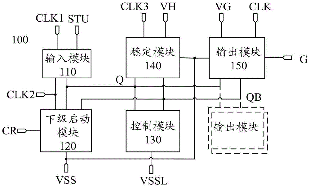
图1示出了根据本发明的实施例的移位寄存器单元100的示意性框图。如图1所示,移位寄存器单元100可包括输入模块110、下级启动模块120、上拉控制模块120、稳定模块140、以及至少一个输出模块(在图1中,仅示出一个输出模块150作为示例,其它输出模块采用虚线框示意性地示出)。FIG. 1 shows a schematic block diagram of a
输入模块110可与第一时钟信号端CLK1、触发信号端STU、上拉节点Q和第二时钟信号端CLK2耦接。输入模块110可根据来自第一时钟信号端CLK1的第一时钟信号和来自触发信号端STU的触发信号,控制上拉节点Q的电压。具体地,输入模块110可在来自第一时钟信号端CLK1的第一时钟信号的控制下,将来自触发信号端STU的触发信号提供至上拉节点Q。The
下级启动模块120可与上拉节点Q、第二时钟信号端CLK2、下拉节点QB、第一电压信号端VSS和下级启动信号输出端CR耦接。下级启动模块120可根据上拉节点Q的电压、下拉节点QB的电压、来自第二时钟信号端CLK2的第二时钟信号、以及来自第一电压信号端VSS的第一电压信号,控制下级启动信号输出端CR的电压。具体地,下级启动模块120可在上拉节点Q的电压的控制下,将来自第二时钟信号端CLK2的第二时钟信号提供至下级启动信号输出端CR,以及下拉节点QB的电压的控制下,将来自第一电压信号端VSS的第一电压信号提供至下级启动信号输出端CR。The lower-level enable
控制模块130可与上拉节点Q、下拉节点QB和第二电压信号端VSSL耦接。控制模块130可根据上拉节点Q的电压和来自第二电压信号端VSSL的第二电压信号控制下拉节点QB的电压,以及根据下拉节点QB的电压和第二电压信号控制上拉节点Q的电压。具体地,控制模块130可在上拉节点Q的电压的控制下,将来自第二电压信号端VSSL的第二电压信号提供至下拉节点QB,以及在下拉节点QB的电压的控制下,将来自第二电压信号端VSSL的第二电压信号提供至上拉节点Q。The
稳定模块140可与第三时钟信号端CLK3、第一电压信号端VSS、第三电压信号端VH、上拉节点Q和下拉节点QB耦接。稳定模块140可根据来自第三时钟信号端CLK3的第三时钟信号、来自第一电压信号端VSS的第一电压信号VSS、以及来自第三电压信号端VH的第三电压信号,控制上拉节点Q的电压和下拉节点QB的电压。具体地,稳定模块140可在来自第三时钟信号端CLK3的第三时钟信号的控制下,将来自第一电压信号端VSS的第一电压信号提供至上拉节点Q,以及在来自第三时钟信号端CLK3的第三时钟信号的控制下,将来自第三电压信号端VH的第三电压信号提供至下拉节点QB。The
根据本发明的实施例的移位寄存器单元100可包括至少一个输出模块,至少一个输出模块中的每个输出模块被配置为根据上拉节点Q的电压、下拉节点QB的电压、第一电压信号VSS、来自各自的控制时钟信号端CLK的控制时钟信号、以及来自各自的控制电压信号端VG的控制电压信号,控制各自的信号输出端G的电压。The
如图1所示,以移位寄存器单元100包括一个输出模块150为例。输出模块150可与上拉节点Q、下拉节点QB、第一电压信号端VSS、控制时钟信号端CLK、控制电压信号端VG和信号输出端G耦接。输出模块150可根据上拉节点Q的电压、下拉节点QB的电压、第一电压信号VSS、来自控制时钟信号端CLK的控制时钟信号、以及来自控制电压信号端VG的控制电压信号,控制信号输出端G的电压。具体地,输出模块150可在上拉节点Q的电压的控制下,将来自控制电压信号端VG的控制电压信号提供至信号输出端G,以及在下拉节点Q的控制下,将来自第一电压信号端VSS的第一电压信号提供至信号输出端G。As shown in FIG. 1 , it is taken as an example that the
在本发明的实施例中,在第一时钟信号的高电平结束时,第二时钟信号的高电平开始,在第二时钟信号的高电平结束时,第三时钟信号的高电平开始。In the embodiment of the present invention, when the high level of the first clock signal ends, the high level of the second clock signal starts, and when the high level of the second clock signal ends, the high level of the third clock signal start.
目前,移位寄存器单元通常在一个触发信号的控制下触发一个移位寄存信号,即输出一路栅极驱动信号,因此仅能满足一行像素的驱动。整个栅极驱动电路使用的移位寄存器单元较多,导致占用面积大且成本高。At present, the shift register unit usually triggers one shift register signal under the control of one trigger signal, that is, outputs one gate driving signal, so it can only satisfy the driving of one row of pixels. The entire gate driving circuit uses many shift register units, resulting in a large occupied area and high cost.
根据本发明的实施例,移位寄存器单元可以在一个触发信号STU的控制下,输出至少一个栅极驱动信号,即触发至少一个移位寄存信号,通过控制各自的控制时钟信号对各自的输出信号进行调整,结构简单,减小显示装置中所使用的移位寄存器单元的数量。According to an embodiment of the present invention, the shift register unit can output at least one gate driving signal under the control of a trigger signal STU, that is, trigger at least one shift register signal, and control the respective control clock signals to the respective output signals by controlling the respective control clock signals. The adjustment is performed, the structure is simple, and the number of shift register units used in the display device is reduced.
应注意的是,用于控制下级启动模块120的第二时钟信号CLK2并不是持续提供高电平,而仅在工作时提供高电平,因此可以降低移位寄存器单元的功耗。It should be noted that the second clock signal CLK2 for controlling the lower-
图2示出了根据本发明的另一实施例的移位寄存器单元200的示意性框图。如图2所示,移位寄存器单元200的输入模块110、下级启动模块120、控制模块130、稳定模块140与图1所示的移位寄存器单元100相同。此外,移位寄存器单元200还包括第一输出模块151和第二输出模块152。FIG. 2 shows a schematic block diagram of a
第一输出模块151可与上拉节点Q、下拉节点QB、第一电压信号端VSS、第一控制时钟信号端CLKA、第一控制电压信号端VG1和第一信号输出端G1耦接。第一输出模块151可根据上拉节点Q的电压、下拉节点QB的电压、来自第一电压信号端VSS的第一电压信号、来自第一控制时钟信号端CLKA的第一控制时钟信号、以及来自第一控制电压信号端VG1的第一控制电压信号,控制第一信号输出端G1的电压。具体地,第一输出模块151可在来自上拉节点Q的电压的控制下,将来自第一控制电压信号端VG1的第一控制电压信号提供至第一信号输出端G1,或者在下拉节点QB的控制下,将来自第一电压信号端VSS的第一电压信号提供至第一信号输出端G1。The
第二输出模块152可与上拉节点Q、下拉节点QB、第一电压信号端VSS、第二控制时钟信号端CLKB、第二控制电压信号端VG2和第二信号输出端G2耦接。第二输出模块152可根据上拉节点Q的电压、下拉节点QB的电压、来自第一电压信号端VSS的第一电压信号、来自第二控制时钟信号端CLKB的第二控制时钟信号、以及来自第二控制电压信号端VG2的第二控制电压信号,控制第二信号输出端G2的电压。具体地,第二输出模块152可在来自上拉节点Q的电压的控制下,将来自第二控制电压信号端VG2的第二控制电压信号提供至第二信号输出端G2,或者在下拉节点QB的控制下,将来自第一电压信号端VSS的第一电压信号提供至第二信号输出端G2。The
在本发明的实施例中,来自第一电压信号端VSS的第一电压信号和来自第二电压信号端VSSL的第二电压信号是低电平信号,来自第三电压信号端VH的第三电压信号、来自第一控制电压信号端VG1的第一控制电压信号和来自第二控制电压信号端VG2的第二控制电压信号是高电平信号。In the embodiment of the present invention, the first voltage signal from the first voltage signal terminal VSS and the second voltage signal from the second voltage signal terminal VSSL are low-level signals, and the third voltage from the third voltage signal terminal VH The signal, the first control voltage signal from the first control voltage signal terminal VG1 and the second control voltage signal from the second control voltage signal terminal VG2 are high-level signals.
根据本发明的实施例,移位寄存器单元可以在一个触发信号STU的控制下,输出两个栅极驱动信号(例如,G1和G2),即触发两个移位寄存信号,通过第一控制时钟信号CLKA和第二控制时钟信号CLKB对输出信号进行调整,结构简单,减小显示装置中所使用的移位寄存器单元的数量。According to an embodiment of the present invention, the shift register unit can output two gate driving signals (eg, G1 and G2) under the control of one trigger signal STU, that is, trigger the two shift register signals, through the first control clock The signal CLKA and the second control clock signal CLKB adjust the output signal, the structure is simple, and the number of shift register units used in the display device is reduced.
图3示出了图2所示的移位寄存器单元200的示例性电路图。在实施例中,所采用的晶体管可以是N型晶体管或者P型晶体管。具体地,晶体管可以是N型或P型场效应晶体管(MOSFET),或者N型或P型双极性晶体管(BJT)。在本发明的实施例中,晶体管的栅极被称为控制极。由于晶体管的源极和漏极是对称的,因此对源极和漏极不做区分,即晶体管的源极可以为第一极(或第二极),漏极可以为第二极(或第一极)。进一步,可以采用具有选通信号输入的任何受控开关器件来实现晶体管的功能,将用于接收控制信号(例如用于开启和关断受控开关器件)的开关器件的受控中间端称为控制极,另外两端分别为第一极和第二极。以下,以N型场效应晶体管(NMOS)为例进行详细的描述。FIG. 3 shows an exemplary circuit diagram of the
在本发明的实施例中,至少一个输出模块中的每个输出模块包括上拉晶体管、下拉晶体管和控制晶体管。上拉晶体管的控制极与上拉节点耦接,其第一极与控制电压信号端耦接,其第二极与信号输出端耦接。下拉晶体管的控制极与下拉节点耦接,其第一极与第一电压信号端耦接,其第二极与信号输出端耦接。控制晶体管的控制极与控制时钟信号端耦接,其第一极与第一电压信号端耦接,其第二极与信号输出端耦接。In an embodiment of the present invention, each of the at least one output module includes a pull-up transistor, a pull-down transistor, and a control transistor. The control electrode of the pull-up transistor is coupled to the pull-up node, the first electrode of the pull-up transistor is coupled to the control voltage signal end, and the second electrode of the pull-up transistor is coupled to the signal output end. The control electrode of the pull-down transistor is coupled to the pull-down node, the first electrode of the pull-down transistor is coupled to the first voltage signal end, and the second electrode of the pull-down transistor is coupled to the signal output end. The control electrode of the control transistor is coupled to the control clock signal end, the first electrode of the control transistor is coupled to the first voltage signal end, and the second electrode of the control transistor is coupled to the signal output end.
如图3所示,输入模块110可包括第一晶体管T1、第二晶体管T2和第十二晶体管T12。第一晶体管T1的控制极与第一时钟信号端CLK1耦接,其第一极与触发信号端STU耦接,其第二极与第二晶体管T2的第一极耦接。第二晶体管T2的控制极与第一时钟信号端CLK1耦接,其第一极与第一晶体管T1的第二极耦接,其第二极与上拉节点Q耦接。第十二晶体管T12的控制极与上拉节点Q耦接,其第一极与第二晶体管T2的第一极耦接,其第二极与第二时钟信号端CLK2耦接。As shown in FIG. 3 , the
下级启动模块120包括第四晶体管T4、第五晶体管T5和第一电容器C。第四晶体管T4的控制极与上拉节点Q耦接,其第一极与第二时钟信号端CLK2耦接,其第二极与下级启动信号输出端CR耦接。第五晶体管T5的控制极与下拉节点QB耦接,其第一极与第一电压信号端VSS耦接,其第二极与下级启动信号输出端CR耦接。第一电容器C被耦接在上拉节点Q和下级启动信号输出端CR之间。The lower-
控制模块130包括第三晶体管T3和第十五晶体管T15。第三晶体管T3的控制极与下拉节点QB耦接,其第一极与第二电压信号端VSSL耦接,其第二极与上拉节点Q耦接。第十五晶体管T15的控制极与上拉节点Q耦接,其第一极与第二电压信号端VSSL耦接,其第二极与下拉节点QB耦接。The
稳定模块140包括第十三晶体管T13和第十四晶体管T14。第十三晶体管T13的控制极与第三时钟信号端CLK3耦接,其第一极与第一电压信号端VSS耦接,其第二极与上拉节点Q耦接。第十四晶体管T14的控制极与第三时钟信号端CLK3耦接,其第一极与第三电压信号端VH耦接,其第二极与下拉节点QB耦接。The
第一输出模块151包括第六晶体管T6(相当于上拉晶体管)、第七晶体管T7(相当于下拉晶体管)和第八晶体管T8(相当于控制晶体管)。第六晶体管T6的控制极与上拉节点Q耦接,其第一极与第一控制电压信号端VG1耦接,其第二极与第一信号输出端(即,第七晶体管T7的第二极)耦接。第七晶体管T7的控制极与下拉节点QB耦接,其第一极与第一电压信号端VSS耦接,其第二极与第六晶体管T6的第二极耦接。第八晶体管T8的控制极与第一控制时钟信号端CLKA耦接,其第一极与第一电压信号端VSS耦接,其第二极与第六晶体管T6的第二极耦接。在本发明的实施例中,第七晶体管T7的宽长比是第六晶体管T6的宽长比的整数倍。The
第二输出模块152包括第九晶体管T9(相当于上拉晶体管)、第十晶体管T10(相当于下拉晶体管)和第十一晶体管T11(相当于控制晶体管)。第九晶体管T9的控制极与上拉节点Q耦接,其第一极与第二控制电压信号端VG2耦接,其第二极与第二信号输出端(即,第十晶体管T10的第二极)耦接。第十晶体管T10的控制极与下拉节点QB耦接,其第一极与第一电压信号端VSS耦接,其第二极与第九晶体管T9的第二极耦接。第十一晶体管T11的控制极与第二控制时钟信号信号端CLKB耦接,其第一极与第一电压信号端VSS耦接,其第二极与第九晶体管T9的第二极耦接。在本发明的实施例中,第十晶体管T10的宽长比是第九晶体管T9的宽长比的整数倍。The
下面结合图4所示的时序图,对如图3所示的移位寄存器单元的工作过程进行详细描述。在以下的描述中,以移位寄存器单元中的晶体管均是N型晶体管为例。第一电压信号VSS和第二电压信号VSSL是低电平信号,第三电压信号VH、第一控制电压信号VG1和第二控制电压信号VG2是高电平信号。The working process of the shift register unit shown in FIG. 3 will be described in detail below with reference to the timing diagram shown in FIG. 4 . In the following description, the transistors in the shift register unit are all N-type transistors as an example. The first voltage signal VSS and the second voltage signal VSSL are low-level signals, and the third voltage signal VH, the first control voltage signal VG1 and the second control voltage signal VG2 are high-level signals.
在图4所示的示例中,第一控制时钟信号CLKA和第二控制时钟信号CLKB是低电平(VGL)。因此,第八晶体管T8和第十一晶体管T11保持截止状态。In the example shown in FIG. 4, the first control clock signal CLKA and the second control clock signal CLKB are low level (VGL). Therefore, the eighth transistor T8 and the eleventh transistor T11 maintain an off state.
在第一时间段(P1),第一时钟信号CLK1是高电平,第二时钟信号CLK2是低电平,第三时钟信号CLK3是低电平,触发信号STU是高电平。在P1期间,输入模块110的第一晶体管T1和第二晶体管T2导通,触发信号STU被提供至上拉节点Q,使上拉节点Q的电压升高。第十五晶体管T15导通,第二电压信号VSSL被提供至下拉节点QB,即下拉节点QB的电压被拉低,使得第三晶体管T3、第五晶体管T5、第七晶体管T7和第十晶体管T10截止。在上拉节点Q的电压的控制下,通过控制第七晶体管T7与第六晶体管T6的宽长比的比例、以及第十晶体管T10与第九晶体管T9的宽长比的比例,使第一信号输出端G1和第二信号输出端G2均输出低电平信号。第四晶体管T4导通,将第二时钟信号CLK2提供至下级启动信号输出端CR,即下级启动信号输出端CR也输出低电平信号。在实际的仿真中,在P1期间,下级启动信号输出端CR、第一信号输出端G1和第二信号输出端G2所输出的信号略有浮动,但仍可认为是低电平信号。在示例中,设定第七晶体管T7的宽长比为第六晶体管T6的宽长比的整数倍,设定第十晶体管T10的宽长比为第九晶体管T9的宽长比的整数倍。During the first period (P1), the first clock signal CLK1 is at a high level, the second clock signal CLK2 is at a low level, the third clock signal CLK3 is at a low level, and the trigger signal STU is at a high level. During P1, the first transistor T1 and the second transistor T2 of the
在第二时间段(P2),第一时钟信号CLK1是低电平,第二时钟信号CLK2是高电平,第三时钟信号CLK3是低电平,触发信号STU是低电平。由于在P1期间,上拉节点Q的电压升高到足以使第四晶体管T4导通,因此第二时钟信号CLK2通过第四晶体管T4传递至下级启动信号输出端CR,因此下级启动信号输出端CR输出高电平信号。通过电容器C,上拉节点Q的电压由于自举作用(bootstrapping)而被进一步上拉至高电平。第十二晶体管T12导通,将第二时钟信号CLK2提供至第一晶体管T1和第二晶体管T2之间的节点,从而使第二晶体管T2关闭地更彻底,进一步降低上拉节点Q的漏电流。此外,第六晶体管T6和第九晶体管T9导通,将第一控制电压信号VG1和第二控制电压信号VG2分别提供至第一信号输出端G1和第二信号输出端G2。在上拉节点Q处于第三电平信号的情况下,第十五晶体管T15保持导通,控制下拉节点QB的电压为低电平,因此,第五晶体管T5、第七晶体管T7和第十晶体管T10保持截止。下级启动信号输出端CR、第一信号输出端G1和第二信号输出端G2输出稳定的高电平信号。During the second period (P2), the first clock signal CLK1 is at a low level, the second clock signal CLK2 is at a high level, the third clock signal CLK3 is at a low level, and the trigger signal STU is at a low level. Since the voltage of the pull-up node Q is raised enough to turn on the fourth transistor T4 during the period P1, the second clock signal CLK2 is transmitted to the lower stage start signal output terminal CR through the fourth transistor T4, so the lower stage start signal output terminal CR Output high level signal. Through the capacitor C, the voltage of the pull-up node Q is further pulled up to a high level due to bootstrapping. The twelfth transistor T12 is turned on to provide the second clock signal CLK2 to the node between the first transistor T1 and the second transistor T2, so that the second transistor T2 is turned off more thoroughly and further reduces the leakage current of the pull-up node Q . In addition, the sixth transistor T6 and the ninth transistor T9 are turned on to supply the first control voltage signal VG1 and the second control voltage signal VG2 to the first signal output terminal G1 and the second signal output terminal G2, respectively. When the pull-up node Q is at the third level signal, the fifteenth transistor T15 is kept on, and the voltage of the pull-down node QB is controlled to be at a low level. Therefore, the fifth transistor T5, the seventh transistor T7 and the tenth transistor T10 remains off. The lower-level start signal output terminal CR, the first signal output terminal G1 and the second signal output terminal G2 output stable high-level signals.
在第三时间段(P3),第一时钟信号CLK1是低电平,第二时钟信号CLK2是低电平,第三时钟信号CLK3是高电平,触发信号STU是低电平。在P3期间,第十三晶体管T13和第十四晶体管T14导通,将第一电压信号VSS提供至上拉节点Q,将第三电压信号VH提供至下拉节点QB,也就是说,上拉节点Q的电压被拉低,下拉节点QB的电压被拉高。第四晶体管T4、第六晶体管T6和第九晶体管T9截止,第五晶体管T5、第七晶体管T7和第十晶体管T10导通。下级启动信号输出端CR输出低电平信号,第一信号输出端G1输出低电平信号,第二信号输出端G2输出低电平信号。In the third period (P3), the first clock signal CLK1 is at a low level, the second clock signal CLK2 is at a low level, the third clock signal CLK3 is at a high level, and the trigger signal STU is at a low level. During P3, the thirteenth transistor T13 and the fourteenth transistor T14 are turned on, supply the first voltage signal VSS to the pull-up node Q, and supply the third voltage signal VH to the pull-down node QB, that is, the pull-up node Q The voltage of the pull-down node QB is pulled high. The fourth transistor T4, the sixth transistor T6 and the ninth transistor T9 are turned off, and the fifth transistor T5, the seventh transistor T7 and the tenth transistor T10 are turned on. The lower-level start signal output terminal CR outputs a low-level signal, the first signal output terminal G1 outputs a low-level signal, and the second signal output terminal G2 outputs a low-level signal.
在随后的时间段,第一时钟信号CLK1、第二时钟信号CLK2和第三时钟信号CLK3的高电平依次被提供,触发信号STU保持为低电平,下级启动信号输出端CR、第一信号输出端G1和第二信号输出端G2保持输出低电平信号。In the following time period, the high levels of the first clock signal CLK1, the second clock signal CLK2 and the third clock signal CLK3 are sequentially provided, the trigger signal STU remains at a low level, the lower-level start signal output terminal CR, the first signal The output terminal G1 and the second signal output terminal G2 keep outputting low-level signals.
在本发明的另一实施例中,第一控制时钟信号CLKA和第二控制时钟信号CLKB中的一者是低电平,另一者是高电平。例如,第一控制时钟信号CLKA是低电平(VGL),并且第二控制时钟信号CLKB是高电平(VGH)。因此,第八晶体管T8截止,第十一晶体管T11导通。如图5所示,第一信号输出端G1输出的第一输出信号与图4相同,第二信号输出端G2保持输出低电平信号。In another embodiment of the present invention, one of the first control clock signal CLKA and the second control clock signal CLKB is at a low level, and the other is at a high level. For example, the first control clock signal CLKA is a low level (VGL), and the second control clock signal CLKB is a high level (VGH). Therefore, the eighth transistor T8 is turned off, and the eleventh transistor T11 is turned on. As shown in FIG. 5 , the first output signal output by the first signal output terminal G1 is the same as that in FIG. 4 , and the second signal output terminal G2 keeps outputting a low-level signal.
可选地,在第一控制时钟信号CLKA是高电平(VGH),并且第二控制时钟信号CLKB是低电平(VGL)时,第八晶体管T8导通,第十一晶体管T11截止。第一信号输出端G1输出保持低电平信号,第二信号输出端G2输出的第二输出信号与图4相同。Optionally, when the first control clock signal CLKA is at a high level (VGH) and the second control clock signal CLKB is at a low level (VGL), the eighth transistor T8 is turned on and the eleventh transistor T11 is turned off. The first signal output terminal G1 outputs a low-level signal, and the second output signal output by the second signal output terminal G2 is the same as that shown in FIG. 4 .
因此,可以通过对第一控制时钟信号CLKA和第二控制时钟信号CLKB进行对应调整,来控制两个输出信号。Therefore, the two output signals can be controlled by correspondingly adjusting the first control clock signal CLKA and the second control clock signal CLKB.
在本发明的实施例中,第一时钟信号CLK1、第二时钟信号CLK2和第三时钟信号CLK3可具有相同的时钟周期,并且占空比均为1:3。In the embodiment of the present invention, the first clock signal CLK1 , the second clock signal CLK2 and the third clock signal CLK3 may have the same clock period, and the duty ratios are all 1:3.
图6是用于驱动根据本发明的实施例的移位寄存器单元的方法的示意性流程图,其中,至少一个输出模块中的每个输出模块的控制时钟信号端的控制时钟信号为低电平信号。在本发明的实施例中,第一电压信号VSS和第二电压信号VSSL是低电平信号,第三电压信号VH和至少一个输出模块中的各个控制电压信号VG是高电平信号。6 is a schematic flowchart of a method for driving a shift register unit according to an embodiment of the present invention, wherein the control clock signal at the control clock signal terminal of each output module in the at least one output module is a low level signal . In the embodiment of the present invention, the first voltage signal VSS and the second voltage signal VSSL are low-level signals, and the third voltage signal VH and each control voltage signal VG in the at least one output module are high-level signals.
在步骤S610,在第一时间段,通过第一时钟信号端输入第一时钟信号(例如,高电平信号),通过触发信号端输入触发信号,使输入模块导通,上拉节点的电压升高,控制模块使下拉节点的电压为低电平,下级启动模块的下级启动信号输出端输出低电平信号,各个输出模块的信号输出端输出低电平信号。In step S610, in the first time period, a first clock signal (eg, a high-level signal) is input through the first clock signal terminal, and a trigger signal is input through the trigger signal terminal, so that the input module is turned on, and the voltage of the pull-up node rises. High, the control module makes the voltage of the pull-down node low, the lower-level startup signal output terminal of the lower-level startup module outputs a low-level signal, and the signal output terminals of each output module output a low-level signal.
在步骤S620,在第二时间段,通过第二时钟信号端输入第二时钟信号(例如,高电平信号),使下级启动模块导通,下级启动模块的下级启动信号输出端输出高电平信号,上拉节点的电压再次升高至高电平,下拉节点的电压保持为低电平,各个输出模块的信号输出端输出高电平信号。In step S620, in the second period of time, a second clock signal (eg, a high-level signal) is input through the second clock signal terminal, so that the lower-level startup module is turned on, and the lower-level startup signal output terminal of the lower-level startup module outputs a high level signal, the voltage of the pull-up node rises to a high level again, the voltage of the pull-down node remains at a low level, and the signal output terminals of each output module output a high-level signal.
在步骤S630,在第三时间段,通过第三时钟信号端输入第三时钟信号(例如,高电平信号),稳定模块导通,使上拉节点的电压变为低电平,下拉节点的电压变为高电平,下级启动模块的下级启动信号输出端输出低电平信号,各个输出模块的信号输出端输出低电平信号。In step S630, in the third time period, a third clock signal (eg, a high-level signal) is input through the third clock signal terminal, the stabilization module is turned on, the voltage of the pull-up node becomes a low level, and the voltage of the pull-down node is turned on. When the voltage becomes a high level, the lower-level startup signal output terminal of the lower-level startup module outputs a low-level signal, and the signal output terminals of each output module output a low-level signal.
在本发明的另一实施例中,至少一个输出模块中的一个或多个输出模块的控制时钟信号端的控制时钟信号为高电平信号。在这种情况下,该一个或多个输出模块的信号输出端输出低电平信号。In another embodiment of the present invention, the control clock signal at the control clock signal terminal of one or more output modules in the at least one output module is a high-level signal. In this case, the signal output terminal of the one or more output modules outputs a low-level signal.
由上,根据本发明的实施例可以通过改变至少一个输出模块中的一个或多个输出模块的控制时钟信号端的控制时钟信号,在一个触发信号的控制下,输出一个或多个驱动信号。此外,根据本发明的实施例还可减小漏电流、降低器件功耗。From the above, according to the embodiment of the present invention, one or more driving signals can be output under the control of a trigger signal by changing the control clock signal of the control clock signal terminal of one or more output modules in the at least one output module. In addition, according to the embodiments of the present invention, leakage current and power consumption of the device can also be reduced.
通常,OLED显示面板正常工作时可能出现阈值电压Vth不稳定的情况,在这种情况下长时间工作会出现阈值电压Vth的偏移。因此,OLED显示面板的像素电路设计需要考虑阈值电压Vth补偿、迁移率补偿和光学补偿。根据本发明的实施例的移位寄存器单元可应用于诸如AMOLED3T1C像素电路,以更好地进行外部补偿。Generally, the threshold voltage Vth may be unstable during normal operation of the OLED display panel, and in this case, the threshold voltage Vth may be shifted during long-term operation. Therefore, the pixel circuit design of the OLED display panel needs to consider threshold voltage Vth compensation, mobility compensation and optical compensation. The shift register unit according to the embodiment of the present invention can be applied to pixel circuits such as AMOLED3T1C for better external compensation.
图7示出了3T1C像素电路的电路图。如图4所示,3T1C电路包括开关晶体管TFT1、感测晶体管TFT2、驱动晶体管TFT3、存储电容器CST和发光二极管OLED。开关晶体管TFT1、感测晶体管TFT2、驱动晶体管TFT3均为N型晶体管TFT。Figure 7 shows a circuit diagram of a 3T1C pixel circuit. As shown in FIG. 4, the 3T1C circuit includes a switching transistor TFT1, a sensing transistor TFT2, a driving transistor TFT3, a storage capacitor CST and a light emitting diode OLED. The switching transistor TFT1, the sensing transistor TFT2, and the driving transistor TFT3 are all N-type transistors TFT.
开关晶体管TFT1的控制极耦接图2所示的移位寄存器单元200的第一信号输出端G1,其第一极耦接数据写入信号Data,其第二极耦接驱动晶体管TFT3的控制极。感测晶体管TFT2的控制极耦接图2所示的移位寄存器单元的第二信号输出端G2,其第一极耦接感测信号Sense,其第二极耦接驱动晶体管TFT3的第二极。驱动晶体管TFT3的第一极耦接高电平信号VDD。存储电容器CST被耦接在开关晶体管TFT1的第二极和驱动晶体管TFT3的第二极之间。发光二极管OLED的阳极耦接驱动晶体管TFT3的第二极,阴极耦接低电平信号VSS。The control electrode of the switching transistor TFT1 is coupled to the first signal output terminal G1 of the
在本发明的实施例中,在正常写入阶段,先对第一输出信号G1和第二输出信号G2进行置位,即第一控制时钟信号CLKA和第二控制时钟信号CLKB均为低电平,由此在上述第二时间段,使第一输出信号G1和第二输出信号G2均为高电平。较短时间后,第一控制时钟信号CLKA保持低电平,将第二控制时钟信号CLKB设置为高电平,以使第一输出信号G1保持为高电平,第二输出信号G2改变为低电平,以进行数据写入。在第一输出信号G1的控制下,将数据写入信号Data传递至开关晶体管TFT1,即驱动晶体管TFT3的控制极,进而在数据写入信号Data的控制下,将高电平信号VDD传递至驱动晶体管TFT3的第二极,由此来驱动发光二极管OLED发光。In the embodiment of the present invention, in the normal writing stage, the first output signal G1 and the second output signal G2 are set first, that is, the first control clock signal CLKA and the second control clock signal CLKB are both low level Therefore, in the above-mentioned second time period, the first output signal G1 and the second output signal G2 are both at a high level. After a short time, the first control clock signal CLKA is kept at a low level, and the second control clock signal CLKB is set at a high level, so that the first output signal G1 is kept at a high level and the second output signal G2 is changed to a low level level for data writing. Under the control of the first output signal G1, the data writing signal Data is transmitted to the switching transistor TFT1, that is, the control electrode of the driving transistor TFT3, and then, under the control of the data writing signal Data, the high-level signal VDD is transmitted to the driving The second pole of the transistor TFT3 drives the light emitting diode OLED to emit light.
在感测补偿阶段,第一控制时钟信号CLKA和第二控制时钟信号CLKB均为低电平,由此在上述第二时间段,第一输出信号G1和第二输出信号G2均保持为高电平。除上述正常写入阶段中将数据写入信号DATA传递至驱动晶体管TFT3的控制极以写入数据的操作外,在第二输出信号G2的控制下,将感测补偿信号Sense传递至感测晶体管TFT2的第二极,即驱动晶体管TFT3的第二极,通过存储电容器CST,驱动晶体管TFT3的控制极的电压被上拉至驱动晶体管TFT3的第二极的电压,从而进一步控制用于驱动发光二极管OLED的电流。In the sensing compensation stage, both the first control clock signal CLKA and the second control clock signal CLKB are at a low level, so that both the first output signal G1 and the second output signal G2 are kept at a high level during the above-mentioned second time period flat. In addition to the operation of transmitting the data writing signal DATA to the control electrode of the driving transistor TFT3 to write data in the normal writing stage, the sensing compensation signal Sense is transmitted to the sensing transistor under the control of the second output signal G2 The second electrode of the TFT2, that is, the second electrode of the driving transistor TFT3, is pulled up to the voltage of the second electrode of the driving transistor TFT3 through the storage capacitor CST, and the voltage of the control electrode of the driving transistor TFT3 is pulled up to further control the voltage used to drive the light-emitting diode. OLED current.
在本发明的实施例中,移位寄存器单元仅在一个触发信号STU的控制下,输出两个驱动信号,即第一输出信号G1和第二输出信号G2,以更好地控制3T1C像素电路。本发明的实施例的移位寄存器单元结构简单,并可以降低功耗和漏电流。In the embodiment of the present invention, the shift register unit outputs two driving signals, namely the first output signal G1 and the second output signal G2 under the control of only one trigger signal STU, to better control the 3T1C pixel circuit. The shift register unit of the embodiment of the present invention has a simple structure, and can reduce power consumption and leakage current.
图8示出根据本发明的实施例的栅极驱动电路800的示意性结构图。如图8所示,栅极驱动电路800可包括多个级联的移位寄存器单元SR1、SR2、…、SRn、SR(n+1)、...。每级移位寄存器单元可以采用如图1所示的移位寄存器单元100的结构。FIG. 8 shows a schematic structural diagram of a
在栅极驱动电路800中,每级移位寄存器单元的端口可包括:第一电压信号端VSS、第二电压信号端VSSL、第三电压信号端VH、至少一个控制电压信号端VG(仅示出一个)、第一时钟信号端CLK1、第二时钟信号端CLK2、第三时钟信号端CLK3、至少一个控制时钟信号端CLK(仅示出一个)、触发信号端STU、下级启动信号输出端CR、以及至少一个信号输出端G(仅示出一个)。In the
各级移位寄存器单元SR(n)的下级启动信号输出端CR与下一级移位寄存器单元SR(n+1)的触发信号端STU耦接。第3n+1级移位寄存器单元的第一时钟信号端与第3n+2级移位寄存器单元的第三时钟信号端和第3n+3级移位寄存器单元的第二时钟信号端耦接,第3n+1级移位寄存器单元的第二时钟信号端与第3n+2级移位寄存器单元的第一时钟信号端和第3n+3级移位寄存器单元的第三时钟信号端耦接,以及第3n+1级移位寄存器单元的第三时钟信号端与第3n+2级移位寄存器单元的第二时钟信号端和第3n+3级移位寄存器单元的第一时钟信号端耦接。n是大于0的整数。The lower stage enable signal output terminal CR of the shift register unit SR(n) of each stage is coupled to the trigger signal terminal STU of the next stage shift register unit SR(n+1). The first clock signal terminal of the 3n+1 stage shift register unit is coupled to the third clock signal terminal of the 3n+2 stage shift register unit and the second clock signal terminal of the 3n+3 stage shift register unit, The second clock signal terminal of the 3n+1 stage shift register unit is coupled to the first clock signal terminal of the 3n+2 stage shift register unit and the third clock signal terminal of the 3n+3 stage shift register unit, and the third clock signal terminal of the 3n+1 stage shift register unit is coupled to the second clock signal terminal of the 3n+2 stage shift register unit and the first clock signal terminal of the 3n+3 stage shift register unit . n is an integer greater than 0.
向第一电压信号端VSS输入低电平的第一电压信号(例如,-8V),向第二电压信号端VSSL输入低电平的第二电压信号(例如,-10V),向第三电压信号端VH输入高电平的第三电压信号(例如,25V)。由此,各个信号输出端G可全摆幅输出,实现输出轨到轨。A first voltage signal of low level (for example, -8V) is input to the first voltage signal terminal VSS, a second voltage signal of low level (for example, -10V) is input to the second voltage signal terminal VSSL, and a third voltage signal is input to the second voltage signal terminal VSSL. The signal terminal VH inputs a high-level third voltage signal (eg, 25V). As a result, each signal output terminal G can be output with full swing to realize output rail-to-rail.
在本发明的实施例中,第一时钟信号的高电平结束时第二时钟信号的高电平开始,以及第二时钟信号的高电平结束时第三时钟信号的高电平开始。进一步地,第一时钟信号、第二时钟信号和第三时钟信号可具有相同的时钟周期,并且占空比均为1:3。In the embodiment of the present invention, the high level of the second clock signal starts when the high level of the first clock signal ends, and the high level of the third clock signal starts when the high level of the second clock signal ends. Further, the first clock signal, the second clock signal and the third clock signal may have the same clock cycle, and the duty ratios are all 1:3.
图9示出了根据本发明的实施例的显示装置900的示意图。显示装置900包括阵列基板950,其中阵列基板950包括图8所示的栅极驱动电路800。显示装置900例如可以是移动电话、平板计算机、显示屏、可穿戴设备等。FIG. 9 shows a schematic diagram of a
以上对本发明的若干实施方式进行了详细描述,但本发明的保护范围并不限于此。显然,对于本领域的普通技术人员来说,在不脱离本发明的精神和范围的情况下,可以对本发明的实施例进行各种修改、替换或变形。本发明的保护范围由所附权利要求限定。Several embodiments of the present invention have been described above in detail, but the protection scope of the present invention is not limited thereto. It is apparent to those skilled in the art that various modifications, substitutions or variations can be made in the embodiments of the present invention without departing from the spirit and scope of the invention. The scope of protection of the present invention is defined by the appended claims.
Claims (17)
Priority Applications (5)
| Application Number | Priority Date | Filing Date | Title |
|---|---|---|---|
| CN201710594509.7A CN109285504B (en) | 2017-07-20 | 2017-07-20 | Shifting register unit, driving method thereof and grid driving circuit |
| JP2018549790A JP6914270B2 (en) | 2017-07-20 | 2018-01-04 | Shift register unit and its drive method, gate drive circuit |
| EP18825852.9A EP3657485A4 (en) | 2017-07-20 | 2018-01-04 | OFFSET REGISTER UNIT AND ITS ATTACK PROCESS AND GRID ATTACK CIRCUIT |
| PCT/CN2018/071296 WO2019015267A1 (en) | 2017-07-20 | 2018-01-04 | Shift register unit and driving method therefor, gate drive circuit |
| US16/312,101 US11087668B1 (en) | 2017-07-20 | 2018-01-04 | Shift register unit and driving method thereof, gate driving circuit |
Applications Claiming Priority (1)
| Application Number | Priority Date | Filing Date | Title |
|---|---|---|---|
| CN201710594509.7A CN109285504B (en) | 2017-07-20 | 2017-07-20 | Shifting register unit, driving method thereof and grid driving circuit |
Publications (2)
| Publication Number | Publication Date |
|---|---|
| CN109285504A CN109285504A (en) | 2019-01-29 |
| CN109285504B true CN109285504B (en) | 2020-07-24 |
Family
ID=65015673
Family Applications (1)
| Application Number | Title | Priority Date | Filing Date |
|---|---|---|---|
| CN201710594509.7A Active CN109285504B (en) | 2017-07-20 | 2017-07-20 | Shifting register unit, driving method thereof and grid driving circuit |
Country Status (5)
| Country | Link |
|---|---|
| US (1) | US11087668B1 (en) |
| EP (1) | EP3657485A4 (en) |
| JP (1) | JP6914270B2 (en) |
| CN (1) | CN109285504B (en) |
| WO (1) | WO2019015267A1 (en) |
Families Citing this family (13)
| Publication number | Priority date | Publication date | Assignee | Title |
|---|---|---|---|---|
| CN109698006B (en) * | 2019-02-19 | 2021-01-26 | 京东方科技集团股份有限公司 | Shift register and driving method thereof, cascade driving circuit and display device |
| CN109830256B (en) * | 2019-03-22 | 2020-12-04 | 京东方科技集团股份有限公司 | A shift register, its driving method, and gate driving circuit |
| CN110114817B (en) * | 2019-03-25 | 2022-09-13 | 京东方科技集团股份有限公司 | Shift register and driving method thereof, grid driving circuit and display device |
| CN110007628B (en) * | 2019-04-10 | 2022-02-01 | 深圳市华星光电半导体显示技术有限公司 | GOA circuit and display panel |
| CN110517619B (en) * | 2019-08-30 | 2023-04-21 | 京东方科技集团股份有限公司 | Shift register unit and driving method thereof, gate driving circuit, display device |
| KR102738325B1 (en) | 2019-10-30 | 2024-12-03 | 엘지디스플레이 주식회사 | Thin film transistor, gate driver including the same, and display device including the same |
| CN110969977A (en) * | 2019-12-02 | 2020-04-07 | 深圳市华星光电半导体显示技术有限公司 | Grid driving circuit, control method thereof and display device |
| US11538395B2 (en) * | 2020-03-18 | 2022-12-27 | Boe Technology Group Co., Ltd. | Shift register unit and driving method thereof, gate drive circuit, and display device |
| CN111540313B (en) * | 2020-05-11 | 2021-10-08 | 京东方科技集团股份有限公司 | Shift register and driving method, driving circuit, display substrate and device |
| CN112542140B (en) | 2020-12-16 | 2022-05-31 | 合肥京东方卓印科技有限公司 | Shift register, gate drive circuit and drive method |
| CN112967652B (en) * | 2021-03-08 | 2023-05-02 | 武汉天马微电子有限公司 | Scanning signal circuit, display panel, display device and driving method |
| CN117642805A (en) * | 2022-06-24 | 2024-03-01 | 京东方科技集团股份有限公司 | Shift register unit, gate driving circuit, display device and driving method |
| KR20240100591A (en) * | 2022-12-22 | 2024-07-02 | 삼성디스플레이 주식회사 | Shift register and display apparatus having the same |
Citations (5)
| Publication number | Priority date | Publication date | Assignee | Title |
|---|---|---|---|---|
| CN101697284A (en) * | 2009-08-24 | 2010-04-21 | 友达光电股份有限公司 | Shift register circuit |
| CN104282287A (en) * | 2014-10-31 | 2015-01-14 | 合肥鑫晟光电科技有限公司 | GOA unit and driving method thereof as well as GOA circuit and display device |
| CN104835476A (en) * | 2015-06-08 | 2015-08-12 | 京东方科技集团股份有限公司 | Shift register unit, grid electrode drive circuit and driving method thereof, and array substrate |
| CN205050536U (en) * | 2015-10-23 | 2016-02-24 | 京东方科技集团股份有限公司 | Shift register unit, shift register and display device |
| CN105609137A (en) * | 2016-01-05 | 2016-05-25 | 京东方科技集团股份有限公司 | Shifting register, grid line integrated drive circuit, array substrate and display device |
Family Cites Families (11)
| Publication number | Priority date | Publication date | Assignee | Title |
|---|---|---|---|---|
| CN102654982B (en) * | 2011-05-16 | 2013-12-04 | 京东方科技集团股份有限公司 | Shift register unit circuit, shift register, array substrate and liquid crystal display |
| KR101340197B1 (en) * | 2011-09-23 | 2013-12-10 | 하이디스 테크놀로지 주식회사 | Shift register and Gate Driving Circuit Using the Same |
| KR102003439B1 (en) * | 2012-12-18 | 2019-07-24 | 엘지디스플레이 주식회사 | Gate shift register and display device using the same |
| KR102066083B1 (en) | 2013-01-31 | 2020-01-15 | 엘지디스플레이 주식회사 | Shift register |
| CN103413514A (en) * | 2013-07-27 | 2013-11-27 | 京东方科技集团股份有限公司 | Shifting register unit, shifting register and displaying device |
| CN104134430B (en) * | 2014-07-04 | 2016-08-17 | 京东方科技集团股份有限公司 | A kind of shift register, gate driver circuit and display device |
| CN104464665B (en) * | 2014-12-08 | 2017-02-22 | 深圳市华星光电技术有限公司 | Scanning driving circuit |
| CN104517575B (en) * | 2014-12-15 | 2017-04-12 | 深圳市华星光电技术有限公司 | Shifting register and level-transmission gate drive circuit |
| KR102281753B1 (en) | 2015-04-14 | 2021-07-27 | 삼성디스플레이 주식회사 | Stage circuit and scan driver using the same |
| CN105609135B (en) | 2015-12-31 | 2019-06-11 | 京东方科技集团股份有限公司 | Shift register unit and driving method thereof, gate driving circuit and display device |
| CN106887217B (en) * | 2017-05-04 | 2020-06-26 | 京东方科技集团股份有限公司 | Shift register unit and control method thereof, gate driving circuit, and display device |
-
2017
- 2017-07-20 CN CN201710594509.7A patent/CN109285504B/en active Active
-
2018
- 2018-01-04 EP EP18825852.9A patent/EP3657485A4/en active Pending
- 2018-01-04 US US16/312,101 patent/US11087668B1/en active Active
- 2018-01-04 WO PCT/CN2018/071296 patent/WO2019015267A1/en not_active Ceased
- 2018-01-04 JP JP2018549790A patent/JP6914270B2/en active Active
Patent Citations (5)
| Publication number | Priority date | Publication date | Assignee | Title |
|---|---|---|---|---|
| CN101697284A (en) * | 2009-08-24 | 2010-04-21 | 友达光电股份有限公司 | Shift register circuit |
| CN104282287A (en) * | 2014-10-31 | 2015-01-14 | 合肥鑫晟光电科技有限公司 | GOA unit and driving method thereof as well as GOA circuit and display device |
| CN104835476A (en) * | 2015-06-08 | 2015-08-12 | 京东方科技集团股份有限公司 | Shift register unit, grid electrode drive circuit and driving method thereof, and array substrate |
| CN205050536U (en) * | 2015-10-23 | 2016-02-24 | 京东方科技集团股份有限公司 | Shift register unit, shift register and display device |
| CN105609137A (en) * | 2016-01-05 | 2016-05-25 | 京东方科技集团股份有限公司 | Shifting register, grid line integrated drive circuit, array substrate and display device |
Also Published As
| Publication number | Publication date |
|---|---|
| JP2020527818A (en) | 2020-09-10 |
| EP3657485A1 (en) | 2020-05-27 |
| WO2019015267A1 (en) | 2019-01-24 |
| CN109285504A (en) | 2019-01-29 |
| US20210225253A1 (en) | 2021-07-22 |
| US11087668B1 (en) | 2021-08-10 |
| EP3657485A4 (en) | 2021-01-13 |
| JP6914270B2 (en) | 2021-08-04 |
Similar Documents
| Publication | Publication Date | Title |
|---|---|---|
| CN109285504B (en) | Shifting register unit, driving method thereof and grid driving circuit | |
| CN111243650B (en) | Shifting register, driving method thereof and grid driving circuit | |
| CN107331351B (en) | Pixel compensation circuit, driving method thereof, display panel and display device | |
| US11875748B2 (en) | Gate driving circuit, display substrate, display device and gate driving method for realizing frequency doubling output | |
| US7978809B2 (en) | Shift register of a display device | |
| CN113178221B (en) | Shift register and driving method thereof, gate driving circuit, and display device | |
| US20140064438A1 (en) | Shift Register, Gate Driving Circuit And Display | |
| CN117012125B (en) | Shift register, gate drive circuit, display panel and electronic device | |
| CN105575327B (en) | A kind of image element circuit, its driving method and organic EL display panel | |
| WO2018129932A1 (en) | Shift register unit circuit and drive method therefor, gate drive circuit, and display device | |
| KR20130132417A (en) | Array substrate row driving unit, array substrate row driving circuit and display device | |
| KR20140067549A (en) | Shift register and method for driving the same | |
| CN111179803A (en) | Shift register and control method thereof, gate drive circuit and display panel | |
| CN114882831A (en) | Display control method of display panel, display module and display device | |
| CN115831059B (en) | Shift register and driving method thereof, grid driving circuit and display device | |
| US20200051654A1 (en) | Shift register unit and driving method thereof, gate driving device | |
| CN102820007B (en) | Array substrate row driving circuit, display panel and display device | |
| JP2010238323A (en) | Shift register and electronic device | |
| WO2025223057A1 (en) | Shift register, light-emission driving circuit, and display apparatus | |
| JP6110177B2 (en) | Shift register circuit and image display device | |
| CN106997755B (en) | Shift register and driving method thereof, gate driving circuit, and display device | |
| CN202720870U (en) | Array substrate row driving circuit, display panel and display device | |
| CN111341261B (en) | Shift register and driving method thereof, signal driving circuit and display device | |
| JP2021504757A (en) | Liquid crystal display panel and its EOA module | |
| JP2014127218A (en) | Shift register circuit and image display device |
Legal Events
| Date | Code | Title | Description |
|---|---|---|---|
| PB01 | Publication | ||
| PB01 | Publication | ||
| SE01 | Entry into force of request for substantive examination | ||
| SE01 | Entry into force of request for substantive examination | ||
| GR01 | Patent grant | ||
| GR01 | Patent grant |