Detailed Description
Embodiments of the present application will be further described below with reference to the accompanying drawings. The same or similar reference numbers in the drawings identify the same or similar elements or elements having the same or similar functionality throughout.
In addition, the embodiments of the present application described below in conjunction with the accompanying drawings are exemplary and are only for the purpose of explaining the embodiments of the present application, and are not to be construed as limiting the present application.
In this application, unless expressly stated or limited otherwise, the first feature "on" or "under" the second feature may be directly contacting the first and second features or indirectly contacting the first and second features through intervening media. Also, a first feature "on," "over," and "above" a second feature may be directly or diagonally above the second feature, or may simply indicate that the first feature is at a higher level than the second feature. A first feature being "under," "below," and "beneath" a second feature may be directly under or obliquely under the first feature, or may simply mean that the first feature is at a lesser elevation than the second feature.
Referring to fig. 1 and fig. 2, an electronic device 1000 according to an embodiment of the present disclosure includes a display screen 10 and a time-of-flight component 20. The electronic device 1000 may further include a housing 30, where the housing 30 may be used to mount functional devices such as the display screen 10 and the time-of-flight assembly 20, and the functional devices may also be a main board, a dual camera module, a receiver, and the like. The specific form of the electronic device 1000 may be a mobile phone, a tablet computer, a smart watch, a head display device, etc., and the electronic device 1000 is used as a mobile phone for description in this application, it is understood that the specific form of the electronic device 1000 is not limited to a mobile phone, and is not limited herein.
The display screen 10 may be mounted on the housing 30, and specifically, the display screen 10 may be mounted on one surface of the housing 30 or both surfaces of the housing 30 opposite to each other. In the example shown in fig. 1, where the display screen 10 is mounted on the front face of the housing 30, the display screen 10 may cover 85% or more of the area of the front face, for example, up to 85%, 86%, 87%, 88%, 89%, 90%, 91%, 92%, 93%, 95% or even 100%. The display screen 10 may be used to display images, which may be text, images, video, icons, etc. information.
Referring to fig. 3, the display screen 10 includes a first sub-screen 11 and a second sub-screen 12, that is, the display screen 10 is composed of two independent sub-screens (the first sub-screen 11 and the second sub-screen 12). When the first sub-screen 11 and the second sub-screen 12 are combined into the display screen 10, human eyes may hardly perceive a boundary line between the first sub-screen 11 and the second sub-screen 12, and when the first sub-screen 11 and the second sub-screen 12 display images, human eyes may not perceive a boundary line between the images displayed by the first sub-screen 11 and the second sub-screen 12 even though the first sub-screen 11 and the second sub-screen 12 display the same frame of image together. The first sub-screen 11 and the second sub-screen 12 can be independently controlled, and in actual use, the first sub-screen 11 and the second sub-screen 12 can be independently controlled and displayed in different display states. Wherein the different display states may be on or off, displayed at different brightness, displayed at different refresh frequencies, etc.
The specific shapes of the first sub-screen 11 and the second sub-screen 12 can be set according to requirements, for example, as shown in fig. 1, the second sub-screen 12 is substantially rectangular, the first sub-screen 11 is also substantially rectangular, and the first sub-screen 11 and the second sub-screen 12 are connected to form a substantially rectangular display screen 10; for example, as shown in fig. 3, the second sub-screen 12 may have a rounded rectangular shape with perforations 121, the first sub-screen 11 may have the same shape as the perforations 121, the perforations 121 may have a racetrack shape, a drop shape, etc., and the first sub-screen 11 and the second sub-screen 12 have complementary shapes and may together form a rounded rectangular display screen 10. Of course, the final shape of the display screen 10, the shape of the first sub-screen 11 or the second sub-screen 12 may also be circular, oval, racetrack, etc., and is not limited herein. The first sub-screen 11 may be located at an edge position of the whole display screen 10, and the second sub-screen 12 may be located at a middle position of the whole display screen 10. The first sub-screen 11 may be used to display status icons of the electronic device 1000, for example, to display battery level, network connection status, system time, and the like of the electronic device 1000. The first sub-screen 11 and the second sub-screen 12 may be of different types.
In one embodiment of the present application, the first sub-screen 11 may be a display screen that emits light through a backlight. The display state of the first sub-screen 11 can be controlled by controlling the light-emitting state of the backlight of the first sub-screen 11, for example, by controlling the backlight to be turned off to control the first sub-screen 11 to be turned off, by controlling the light-emitting luminance of the backlight to control the light-emitting luminance of the first sub-screen 11, and by controlling the light-emitting refresh frequency of the backlight to control the refresh frequency of the first sub-screen 11. Specifically, the first sub-screen 11 may be a Liquid Crystal Display (LCD) or the like that emits light by a backlight. The second sub-screen 12 may be a self-emissive display screen, the second sub-screen 12 comprising a plurality of independently controllable light emitting pixels. The display state of the second sub-screen 12 can be controlled by controlling the light emitting state of the light emitting pixels, for example, by controlling the light emitting pixels at different positions to emit light to control different areas of the second sub-screen 12 to display images, by controlling the light emitting brightness of the light emitting pixels to control the light emitting brightness of the second sub-screen 12, and by controlling the light emitting refresh frequency of the light emitting pixels to control the refresh frequency of the second sub-screen 12. Specifically, the second sub-screen 12 may be one or more of an Organic Light-Emitting Diode (OLED) display screen and a Micro LED display screen.
In another embodiment of the present application, the first sub-screen 11 may be a self-luminous display screen, and the first sub-screen 11 includes a plurality of light-emitting pixels that can be independently controlled. The display state of the first sub-screen 11 can be controlled by controlling the light emitting state of the light emitting pixels, for example, by controlling the light emitting pixels at different positions to emit light to control different areas of the first sub-screen 11 to display images, by controlling the light emitting brightness of the light emitting pixels to control the light emitting brightness of the first sub-screen 11, and by controlling the light emitting refresh frequency of the light emitting pixels to control the refresh frequency of the first sub-screen 11. Specifically, the first sub-screen 11 may be one or more of an Organic Light-Emitting Diode (OLED) display screen and a Micro LED display screen. The second sub-panel 12 may be a display panel that is illuminated by a backlight. The display state of the second sub-screen 12 can be controlled by controlling the light-emitting state of the backlight of the second sub-screen 12, for example, by controlling the backlight to be turned off to control the second sub-screen 12 to be turned off, by controlling the light-emitting brightness of the backlight to control the light-emitting brightness of the second sub-screen 12, and by controlling the light-emitting refresh frequency of the backlight to control the refresh frequency of the second sub-screen 12. Specifically, the second sub-screen 12 may be a Liquid Crystal Display (LCD) or the like that emits light by a backlight.
Referring to fig. 4, the display screen 10 is formed with a front surface 13 and a back surface 14, the front surface 13 is opposite to the back surface 14, light emitted from the display screen 10 is emitted outward in a direction in which the back surface 14 points to the front surface 13, and the light is received by a user after passing through the front surface 13, that is, the user can view an image displayed on the display screen 10 from the front surface 13. Referring to fig. 1, it can be understood that the front surface 13 is a display surface formed by the first sub-screen 11 and the second sub-screen 12, and the back surface is a surface opposite to the display surface formed by the first sub-screen 11 and the second sub-screen 12. The front surface 13 and the back surface 14 may be flat or curved.
Referring to fig. 1, 2 and 4, the time-of-flight component 20 may obtain depth information of a target object by using a time-of-flight distance measurement principle, so as to perform three-dimensional modeling, generate a three-dimensional image, measure distance, and the like. The time of flight module 20 may be mounted in the housing 30 of the electronic device 1000, and specifically, after being mounted on a rack, the rack and the time of flight module 20 may be mounted in the housing 30 together. Time of flight component 20 may include an optical transmitter 21 and an optical receiver 22.
Referring to fig. 1 and 4, the light emitter 21 is disposed on a side of the display screen 10 where the back surface 14 is located, or the light emitter 21 is disposed below the display screen 10, and the laser pulses emitted by the light emitter 21 pass through the display screen 10 and enter the outside. Specifically, the light emitter 21 may include a light source and an optical element, and light (for example, infrared laser) emitted from the light source passes through the optical element, is expanded and emitted, and then passes through the display screen 10 to be projected to the outside. In one example, the transmittance of the display screen 10 may be 60% or more, so that the laser pulses emitted by the light emitter 21 are less lossy when they pass through the display screen 10.
The light receiver 22 may include an infrared sensor, the laser pulse is emitted to the target object, and after being reflected by the target object, the laser pulse can be obtained by the light receiver 22, and the light receiver 22 receives the laser pulse reflected by the target object, and the depth data of the target object can be obtained by combining the time when the light emitter 21 emits the laser pulse. The light receiver 22 may also be arranged on the side of the display screen 10 where the back surface 14 is located, i.e. under the display screen 10, and in particular may be arranged on the same support as the light emitter 21, or the light receiver 22 may be mounted directly on the housing 30. At this time, the light incident surface of the light receiver 22 may be aligned with the display screen 10, and the laser pulse reflected by the target object passes through the display screen 10 and is received by the light receiver 22.
Referring to fig. 1 and 5, in some embodiments, the display screen 10 is formed with a through groove 15, and the through groove 15 does not have a display function. The through-groove 15 penetrates the front surface 13 and the back surface 14. The light emitter 21 of the time-of-flight assembly 20 can be aligned with the through slot 15, that is, the light emitter 21 emits the laser pulse through the through slot 15 and enters the outside, the intensity of the laser pulse entering the outside is not weakened or refracted by the solid part of the display screen 10, and the depth detection of the time-of-flight assembly 20 is accurate.
Specifically, in the example shown in fig. 6, the through-groove 15 includes a notch 151 formed on an edge of the display screen 10, or the through-groove 15 intersects the edge of the display screen 10. The notch 151 may be formed on any one or more of the upper edge, the lower edge, the left edge, the right edge, and the like of the display screen 10. The shape of the notch 151 may be any shape such as triangle, semicircle, rectangle, racetrack, etc., and is not limited herein.
In the example shown in fig. 7, the through-groove 15 includes a through-hole 152 spaced apart from the edge of the display screen 10, or the through-groove 15 opens within the range enclosed by the edge of the display screen 10. The through hole 152 may be located near any one or more of the upper edge, the lower edge, the left edge, the right edge, and the like of the display screen 10. The shape of the through hole 152 may be any shape such as triangle, circle, rectangle, racetrack, etc., and is not limited herein.
In some examples, the through slot 15 may also include the notch 151 and the through hole 152. The number of indentations 151 and through holes 152 may be equal or unequal.
Referring to fig. 5, in some embodiments, the electronic device 1000 further includes a cover 40, and the cover 40 is disposed on a side of the front surface 13 of the display screen 10. When the display screen 10 is provided with the through slots 15, the infrared transmitting layer 50 is disposed on the area of the cover plate 40 corresponding to the through slots 15.
The cover plate 40 may be made of a material having a good light transmission property, such as glass or sapphire. The infrared-transmitting layer 50 may be an infrared-transmitting ink or an infrared-transmitting film, and the infrared-transmitting layer 50 has a high transmittance, for example, a transmittance of 85% or more, to infrared light (for example, light having a wavelength of 940 nm), and has a low transmittance to light other than infrared light or is completely opaque to light other than infrared light. Therefore, it is difficult for a user to see the light emitter 21 aligned with the through-groove 15 through the cover plate 40, and the appearance of the electronic device 1000 is beautiful.
Referring to fig. 8, in some embodiments, the electronic device 1000 further includes a cover plate 40, the cover plate 40 is disposed on a side of the front surface 13 of the display screen 10, and an infrared antireflection film 60 is formed on a region of the cover plate 40 corresponding to the light emitter 21 and the light receiver 22.
The infrared antireflection film 60 may increase the transmittance of infrared light, and when the light emitter 21 emits infrared laser light (i.e., infrared laser pulses) or the light receiver 22 receives laser light, the infrared antireflection film 60 may increase the transmittance of the infrared laser light passing through the cover plate 40, so as to reduce the loss of the infrared laser light passing through the cover plate 40, and further reduce the power consumption of the electronic device 1000. Specifically, the infrared reflection reducing coating 60 may be coated on the upper surface, the lower surface, or both the upper surface and the lower surface of the cover plate 40.
Referring to fig. 9, in some embodiments, an infrared antireflection film 60 is formed on the display screen 10 in the region corresponding to the light emitter 21 and the light receiver 22.
The infrared antireflection film 60 may increase the transmittance of infrared light, and when the light emitter 21 emits infrared laser light or the light receiver 22 receives infrared laser light, the infrared antireflection film 60 may increase the transmittance of infrared laser light passing through the display screen 10, so as to reduce the loss of infrared laser light passing through the display screen 10, thereby reducing the power consumption of the electronic device 1000. Specifically, the infrared reflection reducing coating 60 may be formed on the front surface 13, the back surface 14, or both the front surface 13 and the back surface 14 of the display screen 10. In one example, infrared antireflection film 60 may also be formed inside display panel 10, for example, when first sub-panel 11 is an LCD display panel, infrared antireflection film 60 may be formed on a polarizer in first sub-panel 11, or on an electrode plate of first sub-panel 11, and so on.
Referring to fig. 10, in some embodiments, when the through groove 15 is not formed in the position of the display screen 10 corresponding to the light emitter 21, the infrared transmitting layer 50 is formed in the area of the display screen 10 corresponding to the light emitter 21 and the light receiver 22. As described above, the infrared transmitting layer 50 has a high transmittance to infrared light, but has a low transmittance to light other than infrared light (e.g., visible light) or is completely opaque to light other than infrared light (e.g., visible light), and thus the user cannot see the light emitter 21 and the light receiver 22.
Referring to fig. 11, in some embodiments, the display screen 10 is formed with a through-slot 15 extending through the front surface 13 and the back surface 14. The electronic device 1000 also includes a visible light camera 70, the visible light camera 70 being disposed in alignment with the through slots 15. A visible light reflection reducing coating 80 and/or an infrared cut-off coating 90 are formed on the cover plate 40 in the region corresponding to the through groove 15.
The visible light camera 70 may be used to receive visible light through the cover plate 40 and the through slots 15 to capture images. Forming the visible light antireflection film 80 on the cover plate 40 in the region corresponding to the through groove 15 can increase the transmittance of visible light when the visible light passes through the cover plate 40, so as to improve the imaging quality of the visible light camera 70. Forming the infrared cut film 90 on the cover plate 40 in the region corresponding to the through-groove 15 can reduce the transmittance of infrared light when the infrared light passes through the cover plate 40, or completely prevent the infrared light from entering the visible light camera 70, to reduce the influence of the infrared light on imaging of the visible light camera 70.
In the embodiment shown in fig. 1, time-of-flight assembly 20 is positioned to correspond to first sub-screen 11, i.e., the laser pulses emitted by light emitter 21 pass through first sub-screen 11, and the laser pulses reflected and passing through first sub-screen 11 are received by light receiver 22. When first sub-screen 11 is the LCD display screen, first sub-screen 11 is higher to the transmissivity of infrared light, and optical effect is better for the degree of accuracy of the degree of depth information that time of flight subassembly 20 obtained is higher. The through-groove 15 may be opened on the first sub-screen 11. In one embodiment, the pixel density of the first sub-screen 11 is less than that of the second sub-screen 12, that is, the micro-gap between the pixels of the first sub-screen 11 is greater than that of the second sub-screen 12, the first sub-screen 11 has a smaller blocking effect on light, and the transmittance of light passing through the first sub-screen 11 is higher. Therefore, the transmittance of the laser pulse emitted by the light emitter 21 when the laser pulse passes through the first sub-screen 11 is high, and the transmittance of the reflected laser pulse when the laser pulse passes through the first sub-screen 11 before being received by the light receiver 22 is high. Of course, in other embodiments, the pixel density of the first sub-screen 11 may be greater than or equal to the pixel density of the first sub-screen 11.
Since the display states of the first sub-screen 11 and the second sub-screen 12 can be independently controlled, a user can control the second sub-screen 12 to normally display according to actual requirements, and the first sub-screen 11 is used in cooperation with the optical transmitter 21 or the optical receiver 22. For example, when the light emitter 21 emits a laser pulse or the light receiver 22 receives a reflected laser pulse, the first sub-screen 11 may be turned off, or the display brightness of the first sub-screen 11 may be reduced, or the refresh frequency of the first sub-screen 11 may be adjusted to shift the on-time of the first sub-screen 11 from the on-time of the light emitter 21 or the light receiver 22, so as to reduce the influence of the laser pulse emitted by the light emitter 21 to the scene when the first sub-screen 11 is displayed, or reduce the influence of the reflected laser pulse received by the light receiver 22 when the first sub-screen 11 is displayed. When the optical transmitter 21 or the optical receiver 22 is not enabled, the first sub-screen 11 and the second sub-screen 12 may both be turned on and displayed at the same refresh frequency.
Referring to fig. 12, the control method according to the embodiment of the present disclosure may be used to control the electronic device 1000, where the optical receiver 22 is disposed corresponding to the first sub-screen 11 (as shown in fig. 1), and the control method includes the steps of:
00: determining whether the optical receiver 22 is on; and
01: when the light receiver 22 is turned on, the first sub-screen 11 and the second sub-screen 12 are controlled to display in different display states.
Referring to fig. 13, a control device 400 according to an embodiment of the present disclosure may be used to implement a control method according to an embodiment of the present disclosure. The control device 400 includes a determination module 401 and a control module 402. The determining module 401 may be configured to perform step 00, that is, the determining module 401 may be configured to determine whether the optical receiver 22 is turned on. The control module 402 may be configured to implement step 01, that is, the control module 402 may be configured to control the first sub-screen 11 and the second sub-screen 12 to display in different display states when the optical receiver 22 is turned on.
Referring to fig. 1, in some embodiments, the electronic device 1000 further includes a processor 200, and the processor 200 may be configured to perform the steps 00 and 01 described above, that is, the processor 200 may be configured to determine whether the optical receiver 22 is turned on, and control the first sub-screen 11 and the second sub-screen 12 to display in different display states when the optical receiver 22 is turned on.
When the optical receiver 22 is turned on, that is, when the optical receiver 22 receives the laser pulse reflected back, the first sub-screen 11 and the second sub-screen 12 may be controlled to display in different display states, and a user may control the display state of the first sub-screen 11 to adapt to the use requirement of the optical receiver 22, so as to improve the accuracy of the acquired depth information, and simultaneously control the display state of the second sub-screen 12 to adapt to the viewing requirement of the user, so as to improve the use experience of the user.
It will be appreciated that, in use, the light emitter 21 and the light receiver 22 may be turned on simultaneously, or the time interval between the turning on of the light emitter 21 and the turning on of the light receiver 22 is very small, so that the above-mentioned time when the light receiver 22 is turned on, i.e. the time when the light emitter 21 is turned on, can be considered.
Referring to fig. 14, in some embodiments, step 01 includes step 011: when the light receiver 22 is turned on, the first sub-screen 11 is controlled to be turned off, and the second sub-screen 12 is controlled to be turned on.
Referring to fig. 13, in some embodiments, the control module 402 may be configured to implement step 011, that is, the control module 402 may be configured to control the first sub-screen 11 to be turned off and the second sub-screen 12 to be turned on when the optical receiver 22 is turned on.
Referring to fig. 1, in some embodiments, the processor 200 may be configured to implement step 011, that is, the processor 200 may be configured to control the first sub-screen 11 to be turned off and the second sub-screen 12 to be turned on when the optical receiver 22 is turned on.
When the optical receiver 22 receives the reflected laser pulse, if the first sub-screen 11 is in the on state, the light emitted from the first sub-screen 11 or the light existing inside the first sub-screen 11 may interfere with the optical receiver 22, which affects the accuracy of the depth detection of the time-of-flight component 20. In this embodiment, when the optical receiver 22 is turned on, the first sub-screen 11 is controlled to be turned off, that is, the first sub-screen 11 is controlled not to display an image, so as to avoid interference of the first sub-screen 11 on the optical receiver 22, and meanwhile, the second sub-screen 12 is turned on, so that a user can still obtain information or perform interaction according to the image displayed by the second sub-screen 12, without affecting use of other functions of the electronic device 1000.
Referring to fig. 15, in some embodiments, step 01 includes step 012: when the light receiver 22 is turned on, the first sub-screen 11 is controlled to display at a first brightness, and the second sub-screen 12 is controlled to display at a second brightness, wherein the first brightness is smaller than the second brightness.
Referring to fig. 13, in some embodiments, the control module 402 may further be configured to perform step 012, that is, the control module 402 may be configured to control the first sub-screen 11 to display at a first brightness and the second sub-screen 12 to display at a second brightness when the optical receiver 22 is turned on, where the first brightness is smaller than the second brightness.
Referring to fig. 1, in some embodiments, the processor 200 may be configured to perform step 012, that is, the processor 200 may be configured to control the first sub-screen 11 to display at a first brightness and the second sub-screen 12 to display at a second brightness when the optical receiver 22 is turned on, where the first brightness is smaller than the second brightness.
When the light receiver 22 is turned on, both the first sub-screen 11 and the second sub-screen 12 may be in an on state so as not to affect the integrity of the image displayed by the display screen 10, and meanwhile, the display brightness of the first sub-screen 11 is smaller than that of the second sub-screen 12, so as to reduce the intensity of the light emitted by the first sub-screen 11, thereby reducing the interference to the light receiver 22.
In addition, in some examples, when the light receiver 22 is turned on, the first sub-screen 11 may be controlled to be displayed at the lowest brightness, while the display brightness of the second sub-screen 12 is unchanged; or according to different usage scenarios, when the optical receiver 22 is turned on, the first sub-screen 11 may be controlled to display at different brightness, for example, when a payment scenario has a high requirement on accuracy of depth information acquisition, and when the optical receiver 22 is turned on, the first sub-screen 11 is controlled to display at the lowest brightness; when the scene is unlocked, the accuracy requirement on the acquisition of the depth information is low, and when the optical receiver 22 is turned on, the first sub-screen 11 is controlled to display at a brightness higher than the lowest brightness.
Referring to fig. 12, 14 and 15, in some embodiments, the control method further includes step 02: when the light receiver 22 is turned off, the first sub-screen 11 and the second sub-screen 12 are both controlled to be turned on.
Referring to fig. 13, in some embodiments, the control module 402 may be further configured to perform step 02, that is, the control module 402 may be configured to control both the first sub-screen 11 and the second sub-screen 12 to be turned on when the optical receiver 22 is turned off.
Referring to fig. 1, in some embodiments, the processor 200 may be configured to perform step 02, that is, the processor 200 may be configured to control both the first sub-screen 11 and the second sub-screen 12 to be turned on when the optical receiver 22 is turned off.
When the light receiver 22 is turned off, that is, the user does not need to use the light receiver 22 at this time, that is, the light receiver 22 does not need to receive the laser pulses reflected by and passing through the first sub-screen 11 at this time, therefore, both the first sub-screen 11 and the second sub-screen 12 are controlled to be turned on, so that the whole display screen 10 is used for displaying images, thereby improving the user's appearance when using the electronic device 1000.
Please refer to fig. 1 and fig. 3, it can be understood that, when the first sub-screen 11 and the second sub-screen 12 are both turned on or displayed at different brightness, the picture displayed by the first sub-screen 11 and the picture displayed by the second sub-screen 12 may together form a complete display picture, for example, when the electronic device 1000 is playing a movie, the display screen 10 displays one frame of movie picture, where the movie picture has a tree, a man, and a woman, and the man may be located in the second sub-screen 12, and most of the woman is located in the second sub-screen 12, and the arm is located in the first sub-screen 11. Or; the picture displayed by the first sub-screen 11 and the picture displayed by the second sub-screen 12 are two independent display pictures, for example, when the electronic device 1000 is currently executing a task of playing a movie, the movie picture is displayed on the second sub-screen 12, and the first sub-screen 11 may synchronously display the battery power, the network connection state, the system time, and the like of the electronic device 1000, or synchronously display an instant messaging message or a message notification of each application program, and the like.
The following will describe the specific details of the LCD display screen, the OLED display screen, and the Micro LED display screen when being controlled to emit light:
referring to fig. 16, the LCD panel 93 may include a backlight module 931, a lower polarizer 932, a Thin-film transistor (TFT) substrate 933, a liquid crystal layer 934, a color filter 935, and an upper polarizer 936 arranged in sequence along a light emitting direction. The backlight module 931 may be regarded as a backlight source. The lower polarizer 932 and the upper polarizer 936 are used for controlling the passing or not of the light, and specifically, the upper polarizer 936 and the lower polarizer 932 form a barrier angle respectively, block the component perpendicular to the barrier in the light, and only allow the component parallel to the barrier to pass. TFT substrate 933 is used to provide a conductive path to generate a voltage. The color filter 935 is used to form a color image. The liquid crystal layer 934 includes liquid crystal molecules, and the electro-optic effect caused by the anisotropy of the liquid crystal molecule structure, that is, the anisotropy of the dielectric coefficient and the refractive index of the liquid crystal molecules, is different due to the different directions. The LCD panel 93 generates a voltage through the TFT substrate 933 according to the characteristics of the liquid crystal itself to form an electric field between the upper polarizer 936 and the lower polarizer 932, and controls the rotation of liquid crystal molecules by the electric field to change the traveling direction of light so that the light passes through or is blocked by the lower polarizer 932 and the upper polarizer 936, so that different gray-scale brightness can be formed by different electric fields.
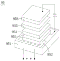
Referring to fig. 17, the OLED display 95 includes a substrate 951, an anode 952, a hole transport layer 953, a light emitting layer 954, an electron transport layer 955, and a cathode 956. Wherein the substrate 951 is used to support the entire OLED display 95. When a voltage is applied to the anode 952 and the cathode 956 of the OLED, electrons and holes are injected from the cathode 956 and the anode 952, respectively, into the organic functional layer sandwiched between the two electrodes. The injected electrons and holes migrate from the electron transport layer 955 and the hole transport layer 953, respectively, to the light emitting layer 954. After the electrons and holes are injected into the light-emitting layer 954, they are bound together by coulomb force to form hole pairs, i.e., excitons. The excitons migrate under the influence of the electric field, transferring energy to the dopant material in the light-emitting layer 954. Electrons in the dopant material of the light-emitting layer 954 absorb energy and then transition from a ground state to an excited state. Since the excited state is unstable, the electron transits from the excited state back to the ground state again, releasing energy in the form of a photon. Depending on the excited state energy level of the luminescent material, the electrons release photons of different energies during the transition back to the ground state, the energy determining the wavelength of the light, the different wavelengths meaning different colors of the light. Thus, the OLED display 95 can emit light of different colors in a self-luminous manner. The luminance or intensity of light emitted by the OLED display 95 depends on the properties of the light-emitting material and the amount of current applied. For the same OLED display screen 95, the greater the current, the higher the brightness of the light. Each pixel (composed of a plurality of sub-pixels that can self-emit light) in the OLED display screen 95 may be controlled to be on/off by an independent thin film transistor, so that each pixel may continuously and independently emit light.
Referring to fig. 18 and 19, the Micro LED display 97 may include a driving substrate 971, an encapsulation substrate 972, a support 973, and a plurality of pixels 974. The driving substrate 971 and the package substrate 972 are disposed opposite to each other, and a plurality of pixels 974 are arranged between the driving substrate 971 and the package substrate 972. A visible light source 9741 is disposed in each pixel 974.
A display driving circuit (not shown) is disposed in the driving substrate 971, and the driving substrate 971 can control on/off and brightness of the light source in each pixel 974. The package substrate 972 is used for protecting the light source, and the material of the package substrate 972 may be plastic with certain hardness, such as polyethylene terephthalate (PET) or Polycarbonate (PC), or may be glass. The support 973 is used to keep a certain distance between the driving substrate 971 and the encapsulation substrate 972 and prevent excessive compression on the pixel 974.
Each pixel 974 further includes a lower pixel electrode 9742 and an upper pixel electrode 9743, the lower pixel electrode 9742 is disposed on the driving substrate 971, the upper pixel electrode 9743 is disposed under the encapsulation substrate 972, and the visible light source 9741 is sandwiched between the lower pixel electrode 9742 and the upper pixel electrode 9743. The material of the pixel electrode may be indium tin oxide or a conductive metal.
As shown in fig. 18, in one example, the plurality of visible light sources 9741 includes a red light source, a green light source, and a blue light source, and each visible light source 9741 and the corresponding pixel electrode form a pixel 974, so that the pixels 974 including different light sources emit light of different colors.
Referring to fig. 19, in another example, the structure of the pixel 974 may also include a visible light source 9741 and a color conversion layer 9744. For example, the plurality of visible light sources 9741 includes a red light source and a blue light source, and each of the visible light sources 9741 emits light of a corresponding color with the pixel 974 formed by the corresponding pixel electrode. The pixel 974 with the red light source emits red light, the pixel 974 with the blue light source emits blue light, and the pixel 974 with the blue light source and the color conversion layer 9744 emits green light. The pixels 974 also include a spacer layer 9745, the spacer layer 9745 facilitating height uniformity between the pixels 974.
To sum up, the LCD panel 93 can display images by controlling the backlight module 931 to emit light, wherein the backlight module 931 of the LCD panel 93 can only be controlled as a whole, i.e., the whole panel emits light or does not emit light; the OLED display 95 can display images by independently controlling the light emitting layers 954 of the pixels to emit light with different colors and brightnesses; the Micro LED display 97 can display images by independently controlling the visible light sources 9741 to emit light with different brightness and different colors.
In the description herein, reference to the description of the term "one embodiment," "some embodiments," "an example," "a specific example," or "some examples," etc., means that a particular feature, structure, material, or characteristic described in connection with the embodiment or example is included in at least one embodiment or example of the application. In this specification, the schematic representations of the terms used above are not necessarily intended to refer to the same embodiment or example. Furthermore, the particular features, structures, materials, or characteristics described may be combined in any suitable manner in any one or more embodiments or examples. Furthermore, various embodiments or examples and features of different embodiments or examples described in this specification can be combined and combined by one skilled in the art without contradiction.
Furthermore, the terms "first", "second" and "first" are used for descriptive purposes only and are not to be construed as indicating or implying relative importance or implicitly indicating the number of technical features indicated. Thus, a feature defined as "first" or "second" may explicitly or implicitly include at least one such feature. In the description of the present application, "plurality" means at least two, e.g., two, three, etc., unless specifically limited otherwise.
Although embodiments of the present application have been shown and described above, it is understood that the above embodiments are exemplary and should not be construed as limiting the present application, and that variations, modifications, substitutions and alterations may be made to the above embodiments by those of ordinary skill in the art within the scope of the present application.