Variable optical filter and wavelength selective sensor based thereon
The present application is a divisional application of the application entitled "variable optical filter and wavelength selective sensor based thereon", having an application date of 2014, month 28, and application number of 201480006294.7.
Technical Field
The present invention relates to optical filters, and in particular to optical filters having spatially varying spectral characteristics.
Background
The transmission wavelength of the spatially variable filter varies in the lateral direction across the filter. By attaching the photodetector array to the spatially variable filter, a compact spectrometer can be constructed. A filter in which the transmission wavelength linearly varies with distance in the lateral direction over the entire filter is called a Linear Variable Filter (LVF). A linear variation of the transmitted wavelength with distance is conveniently achieved, although it is not essential. The spectra obtained with the LVF and constant pitch photodetector arrays have constant wavelength steps.
Pellicori et al, in us patent 4,957,371, disclose a wedge filter spectrometer comprising an LVF having a first plurality of layers of high refractive index material and a second plurality of layers of low refractive index material, the individual high and low refractive index layers overlapping each other and being substantially linearly tapered in thickness to form a linearly variable optical thin film interference filter. The photodetector array is attached to the LVF to form a very compact overall structure.
Anthon, in U.S. patent 6,057,925, discloses a compact spectrometer device comprising a thin film interference LVF and a photodetector array coupled to the LVF by a gradient index lens array or microlens array for use in a color sensing device such as a portable colorimeter. The lightweight and robust construction of the thin film interference LVF based spectrometer enables the portable colorimeter to characterize the color of an object under field conditions.
Weigl et al, in us patent 6,091,502, disclose a compact LVF based spectrometer for fluorescence and absorption spectroscopy measurements with spatial resolution in fluid cells. By placing the LVF in the light path such that the transmittance of the filter changes in the direction of flow, it is possible to determine spectrally the concentration of the staining marker of the protein in the biological cell fluid.
Referring to FIG. 1A, a typical compact spectrometer 100 package using the prior art similar to the spectrometers used in the Pellicori, Anthon and Weigl devicesIncludes an LVF 102 optically coupled to a photodetector array 104. Transmission wavelength lambdaTVaries across LVF 102 in direction 106. In operation, light 108 impinges on the LVF 102. LVF 102 transmits only wavelength λTLight of a narrow band of the surroundings passes through, lambdaTIn a direction 106 parallel to the photodetector array 104. As a result, each photodetector 105 of the photodetector array 104 responds to a different wavelength band of light 108. By measuring the photocurrent of each photodetector 105 of the photodetector array 104, a spectrum of light 108 can be obtained.
The LVF 102 includes a stack of thin films 112 supported by a substrate 110. Referring to fig. 1B, the thin-film stack 112 includes two regions: a blocking region 121 for blocking a wavelength shorter or longer than λTAnd a band pass region 122 for passing only λTA narrow passband centered on the optical transmission. Each of the regions 121 and 122 includes high refractive index layers 131 and low refractive index layers 132 having high refractive indices and low refractive indices, respectively, which are alternately arranged. The material of high index layer 131/low index layer 132 is the same across regions 121 and 122, except for the difference in thickness to achieve the desired optical properties. The blocking region 121 includes a barrier for blocking non- λTA quarter-wave stack of wavelengths, with bandpass region 122 including a region for transmission at λTA half-wavelength stack of a centered narrow passband. The combination of materials in a material pair (material pair) may include metal oxides or fluorides.
One drawback of the LVF 102 is that there is an inherent trade-off between the optical performance of the LVF 102 and the total thickness of the thin film stack 112. To ensure against non-lambdaTHas a good blocking effect and the blocking region 121 must comprise a plurality of layers. For low loss oxides, the number of layers can be up to 100 layers. To ensure lambdaTThe surrounding narrow passband, passband region 122 may also need to include many layers and/or include a thick center layer. The greater thickness of the thin-film stack 112 may increase internal stresses within the thin-film stack 112, causing it to break and/or peel away from the substrate 110. A high index material such as silicon may be used to reduce the total number of layers. However, high index materials typically increase LVF 102Optical losses.
Summary of The Invention
It is an object of the present invention to reduce the trade-off between thickness and optical performance of a variable filter.
The inventors have recognized that there are the following differences between the key optical requirements for the material of the blocking regions and the material of the pass regions of the variable filter. In the blocking region, having a high refractive index contrast is a key requirement. The high refractive index contrast makes it possible to reduce the number of layers and improve the blocking efficiency. Low loss is more important than high index contrast in the band pass region because light undergoes multiple reflections in this region, much more often than in the barrier layer. Thus, providing a low loss, relatively low index material combination in the pass region, while providing a high index contrast, relatively high loss material combination in the block region, can result in a thin, low stress variable optical filter with low optical loss, narrow band transmission peaks, and strong out-of-band rejection.
According to the present invention there is provided an optical filter having a laterally variable transmission wavelength over a range of wavelengths, the optical filter comprising:
a bandpass filter comprising a stack of alternately arranged first and second layers comprising a first material and a second material, respectively, and having a laterally varying thickness for providing said laterally variable transmission wavelength;
a blocking filter comprising a stack of alternating third and fourth layers comprising third and fourth materials, respectively, and having laterally varying thicknesses coordinated with the laterally varying thicknesses of the first and second dielectric layers for blocking wavelengths in a wavelength range that are greater than or less than the laterally variable transmission wavelength;
the first material, the second material and the fourth material respectively comprise different materials, so that the refractive index of the first material is smaller than that of the second material, the refractive index of the second material is smaller than that of the fourth material, and the absorption coefficient of the second material is smaller than that of the fourth material.
Advantageously, the bandpass filter further comprises at least one fifth layer comprising said fourth material, which is arranged in the region of a local minimum of the optical standing wave within the bandpass filter, whereby the blocking wavelength region of the bandpass filter is widened and the thickness of the bandpass filter is reduced.
In one embodiment, the transmission wavelength is monotonically variable along the length dimension of the filter. In a preferred embodiment, the transmission wavelength is logarithmically variable along the length dimension. The first material and the third material may comprise the same material. The filter may comprise 3, 4 or more different materials.
According to the present invention there is also provided a wavelength selective sensor comprising an optical filter as described above and an array of photodetectors coupled to the optical filter. The photodetectors are spaced along the length dimension. As a result, different photodetectors in the array respond to different wavelengths of light incident on the filter from the side opposite the array.
Preferably, the photodetector array includes a substrate for the optical filter. An array of photodetectors is provided, and first through fifth layers are deposited directly on the array to form, respectively, a bandpass filter and a blocking filter supported by the array. Advantages of depositing the filter directly on the array of photodetectors include: the spectral resolution can be improved since the light does not need to be transmitted through a separate bulk substrate; light leakage between adjacent photodetectors is reduced; and improved reliability. The filters may also be produced separately and attached directly to the array, for example using optical epoxy bonding.
There is also provided, in accordance with another embodiment of the present invention, a wavelength selective sensor, in which an array of photodetectors includes a device chip having opposing first and second surfaces. The photodetectors of the array are disposed within a first surface of the device chip, and the optical filter is disposed on the first surface of the device chip above the photodetectors. The wavelength selective sensor can be produced in the following way:
(A) manufacturing a device chip, the manufacturing steps being:
(i) providing a device wafer having opposing first and second surfaces;
(ii) forming the array of photodetectors facing the first surface in a second surface of the device wafer;
(iii) polishing a first surface of a device wafer to expose the photodetectors of the array; and
(B) (iv) depositing first to fifth layers on the first surface of the device wafer polished in step (iii) to form bandpass and blocking filters for the optical filter.
There is also provided, in accordance with another embodiment of the present invention, a method of manufacturing a wavelength selective sensor, including:
(a) providing an array of photodetectors;
(b) depositing on the array of photodetectors
A bandpass filter comprising a stack of alternately arranged first and second layers comprising a first material and a second material, respectively, and having a laterally varying thickness for providing a laterally variable transmission wavelength; and
a blocking filter comprising a stack of alternately arranged third and fourth layers comprising third and fourth materials, respectively, and having laterally varying thicknesses coordinated with the laterally varying thicknesses of the first and second dielectric layers for blocking wavelengths in a wavelength range larger or smaller than the laterally variable transmission wavelength;
the first material, the second material and the fourth material respectively comprise different materials, so that the refractive index of the first material is smaller than that of the second material, the refractive index of the second material is smaller than that of the fourth material, and the absorption coefficient of the second material is smaller than that of the fourth material.
In one embodiment, step (a) comprises:
(i) providing a device wafer having opposing first and second surfaces;
(ii) forming an array of photodetectors in a second surface of the device wafer facing the first surface; and
(iii) polishing a first surface of a device wafer to expose the photodetectors of the array;
wherein in step (b) a bandpass filter and a blocking filter are deposited within the first surface of the device wafer polished in step (iii).
The present application also includes the following aspects:
1) an optical filter having a laterally variable transmission wavelength over a range of wavelengths, the optical filter comprising:
a bandpass filter comprising a stack of alternately arranged first and second layers comprising a first material and a second material, respectively, and having a laterally varying thickness for providing said laterally variable transmission wavelength;
a blocking filter comprising a stack of alternating third and fourth layers comprising third and fourth materials, respectively, and having laterally varying thicknesses coordinated with the laterally varying thicknesses of the first and second layers for blocking wavelengths in a wavelength range that are greater than or less than the laterally variable transmission wavelength;
wherein the first material, the second material, and the fourth material each comprise a different material such that the refractive index of the first material is less than the refractive index of the second material, the refractive index of the second material is less than the refractive index of the fourth material, and the absorption coefficient of the second material is less than the absorption coefficient of the fourth material; and is
Wherein the bandpass filter further comprises at least one fifth layer comprising the fourth material, which is arranged in the region of a local minimum of an optical standing wave within the bandpass filter, whereby the blocking wavelength region of the bandpass filter is widened and the thickness of the bandpass filter is reduced.
2) The optical filter of claim 1), wherein the first material and the third material comprise the same material.
3) The optical filter of claim 2), wherein the first material and the third material comprise the same dielectric material.
4) The optical filter of claim 3), wherein the dielectric material comprises silicon dioxide.
5) The optical filter of claim 1), wherein the fourth material comprises a semiconductor material.
6) The optical filter of claim 5, wherein the semiconductor material comprises silicon, and the first and third materials comprise silicon dioxide.
7) The optical filter of claim 6), wherein the second material is selected from the group consisting of titanium dioxide, tantalum pentoxide, niobium pentoxide, and alloys of tantalum pentoxide and niobium pentoxide.
8) The optical filter of claim 1), wherein the refractive index of the first and third materials is between 1.35 and 1.6, the refractive index of the second material is between 1.8 and 2.5, and the refractive index of the fourth material is between 2.6 and 4.5.
9) The optical filter of claim 8), wherein the wavelength range is from 900nm to 1700nm, and wherein the total thickness of the band-pass filter and the blocking filter at a position corresponding to the transmission wavelength of 1300nm is less than 20 μm.
10) The optical filter of claim 9), further comprising a substrate transparent in the wavelength range; wherein the band pass filter is supported by the blocking filter, which is supported by the substrate.
11) The optical filter of claim 1), wherein the blocking filter comprises a first portion and a second portion for blocking wavelengths larger and smaller than the transmission wavelength, respectively, wherein the band pass filter is disposed on an optical path between the first portion and the second portion of the blocking filter.
12) The optical filter of claim 11), wherein the first material and the third material comprise silicon dioxide, the second material comprises tantalum pentoxide or niobium pentoxide, and the fourth material comprises silicon; wherein the bandpass filter comprises no more than 20 layers, and wherein the blocking filter comprises no more than 60 layers.
13) The optical filter of claim 12), wherein a total thickness of the bandpass filter and the blocking filter is not more than 10 μm.
14) The optical filter of claim 1), wherein the transmission wavelength is monotonically variable along a length dimension of the optical filter.
15) The optical filter of claim 14), wherein the transmission wavelength is logarithmically variable along the length dimension.
16) A wavelength selective sensor comprising:
the optical filter of claim 14); and
an array of photodetectors coupled to the optical filter, wherein the photodetectors are spaced along a length dimension, whereby different photodetectors in the array of photodetectors respond to different wavelengths of light incident on the optical filter from a side opposite the array of photodetectors.
17) The wavelength selective sensor of claim 16), wherein the array of photodetectors comprises a substrate for the optical filter.
18) The wavelength selective sensor of claim 17), wherein the photodetectors have different heights, the array of photodetectors further comprising a planarization layer disposed over the photodetectors, wherein the optical filter is supported by the planarization layer.
19) The wavelength selective sensor of claim 17), wherein the photodetectors are spaced apart by laterally spaced gaps, the array of photodetectors further comprising an opaque insulating material disposed within the gaps for optical insulation of individual photodetectors in the array of photodetectors.
20) The wavelength selective sensor of claim 19), wherein the optical filter comprises a plurality of slots, each of the slots being disposed over a corresponding one of the laterally spaced gaps, wherein the insulating material is disposed within the slots for providing additional optical insulation for individual photodetectors in the array of photodetectors.
21) The wavelength-selective sensor of claim 17), wherein the array of photodetectors comprises a device chip having opposing first and second surfaces, wherein the photodetectors of the array are disposed within the first surface of the device chip, and wherein the optical filter is disposed on the first surface of the device chip above the photodetectors.
22) The wavelength selective sensor of claim 21), wherein the array of photodetectors further comprises a carrier chip bonded to the second surface of the device chip.
23) The wavelength selective sensor of claim 17), wherein the array of photodetectors comprises an array substrate having opposing first and second surfaces, wherein the photodetectors of the array are disposed within the first surface of the array substrate and the optical filter is disposed on the second surface of the array substrate.
24) The wavelength selective sensor of claim 23), further comprising a multiplexer chip for reading out photoelectric signals of the photodetectors of the array, wherein the multiplexer chip is flip-chip bonded onto the first surface of the array substrate.
25) A method of producing the wavelength selective sensor of claim 17), the method comprising
(a) Providing an array of said photodetectors;
(b) depositing first through fifth layers on the array of photodetectors to form the bandpass filters and the blocking filters of the optical filter.
26) A method of producing the wavelength selective sensor of claim 21), the method comprising
(A) Fabricating the device chip, the fabricating comprising:
(i) providing a device wafer having opposing first and second surfaces;
(ii) forming the photodetectors of the array facing the first surface within the second surface of the device wafer;
(iii) polishing the first surface of the device wafer to expose the photodetectors of the array; and
(B) (iv) depositing the first through fifth layers on the first surface of the device wafer polished in step (iii) to form the bandpass and blocking filters of the optical filter.
27) A method of manufacturing a wavelength selective sensor, comprising:
(a) providing an array of photodetectors;
(b) depositing on the array of photodetectors:
a bandpass filter comprising a stack of alternately arranged first and second layers comprising a first material and a second material, respectively, and having a laterally varying thickness for providing a laterally variable transmission wavelength; and
a blocking filter comprising a stack of alternating third and fourth layers comprising third and fourth materials, respectively, and having laterally varying thicknesses coordinated with the laterally varying thicknesses of the first and second layers for blocking wavelengths in a wavelength range that are greater than or less than the laterally variable transmission wavelength;
wherein the first material, the second material, and the fourth material each comprise a different material such that the refractive index of the first material is less than the refractive index of the second material, the refractive index of the second material is less than the refractive index of the fourth material, and the absorption coefficient of the second material is less than the absorption coefficient of the fourth material.
28) The method of 27), wherein step (a) comprises
(i) Providing a device wafer having opposing first and second surfaces;
(ii) forming an array of the photodetectors in the second surface of the device wafer facing the first surface; and
(iii) polishing the first surface of the device wafer to expose the photodetectors of the array;
wherein in step (b) the bandpass filter and the blocking filter are deposited within the first surface of the device wafer polished in step (iii).
Drawings
Exemplary embodiments will now be described with reference to the accompanying drawings, in which:
FIG. 1A is a three-dimensional view of a prior art spectrometer based on a thin film LVF;
FIG. 1B is an enlarged cross-sectional view of the thin-film structure of the LVF of FIG. 1A;
FIG. 2 is a cross-sectional view of a variable optical filter of the present invention on a substrate;
fig. 3A to 3C are transmission spectra of a blocking filter segment and a band pass filter segment of the variable filter of fig. 2 at different positions along a direction of change of transmission wavelength;
FIG. 4A is a schematic cross-sectional view of the filter of FIG. 2 taken along line A-A in FIG. 2, showing a bandpass filter segment and a blocking filter segment;
FIG. 4B is an enlarged cross-sectional view of the bandpass filter segment of the filter of FIG. 4A;
FIGS. 5A and 5B are transmission spectra of bandpass filter segments made of different materials under collimated light illumination (FIG. 5A) and under divergent or convergent light illumination (FIG. 5B);
FIG. 6 is a transmission spectrum of a blocking filter made of a different material;
FIGS. 7A and 7B are space refractive index plots, drawn to the same scale, of a variable optical filter comprising only a low loss oxide (FIG. 7A) and a variable optical filter comprising a combination of materials according to the present invention (FIG. 7B);
FIG. 7C is an enlarged view of the spatial index plot of FIG. 7B;
FIG. 7D is a transmission spectrum of a band pass section of the variable filter of FIGS. 7A and 7B;
FIGS. 8A through 8D are side cross-sectional views of various embodiments of wavelength selective sensors of the present invention including the variable filter of FIG. 2 or FIG. 7B;
FIGS. 9A and 9B are side cross-sectional views of embodiments of a wavelength selective sensor having a back-polished photodetector array (FIG. 9A) and a wavelength selective sensor having a flip-chip multiplexer circuit (FIG. 9B);
fig. 10A to 10C are side cross-sectional views of a wafer including the wavelength selective sensor of fig. 9A at various stages of processing.
Detailed description of the invention
While various embodiments and examples have been described in connection with the present teachings, it is not intended that the present teachings be limited to these embodiments. On the contrary, the present teachings encompass various alternatives, modifications, and equivalents as may be appreciated by those skilled in the art.
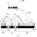
Referring to fig. 2 and fig. 3A, 3B, and 3C, the filter 200 (fig. 2) is positioned at λ1And λ2A laterally variable transmission wavelength λ in the wavelength range therebetweenTWith a narrow pass band 310 (fig. 3A-3C). Transmission wavelength lambdaTVarying along the x-direction as shown in fig. 2. The filter 200 may be disposed on a transparent substrate 202. The variable filter 200 includes a bandpass filter 204 and blocking filters 206A, 206B disposed on a substrate 202. The bandpass filter 204 includes a stack of alternately arranged first layers 211 and second layers 212, the first layers 211 and the second layers 212 including a first material and a second material, respectively. The thickness of the first layer 211 and the second layer 212 varies laterally in the x-direction (fig. 2) for providing a laterally variable transmission wavelength λ of the pass band 310T. Transmission wavelength lambdaTIs approximately proportional to the local thickness of the first layer 211 and the second layer 212. For example, the transmission wavelength λTAt the coordinate x1Close to the wavelength range (lambda) (FIGS. 2 and 3A)1,λ2) Of the shortest wavelength λ1(ii) a At the coordinate x2At (FIGS. 2 and 3B) in the wavelength range (λ)1,λ2) Middle of (d); and at the coordinate x3Where (FIGS. 2 and 3C) the wavelength range (λ) is approached1,λ2) Of longest wavelength λ2。
The blocking filters 206A, 206B each includeA stack of alternately arranged third layers 213 and fourth layers 214, the third layers 213 and the fourth layers 214 comprising a third material and a fourth material, respectively. The third layer 213 and the fourth layer 214 have laterally varying thicknesses coordinated with the laterally varying thicknesses of the first layer 211 and the second layer 212 for blocking a wavelength range (λ)1,λ2) Internal less than or greater than the transversely variable transmission wavelength lambdaTOf (c) is measured. Specifically, the top blocking filter 206A is used to block less than λT(iii) wavelength (left bands 301A, 302A, and 303A in fig. 3A, 3B, and 3C, respectively), the bottom-blocking filter 206B is used to block wavelengths greater than λT(ii) wavelength ( right bands 301B, 302B, and 303B in fig. 3A, 3B, and 3C, respectively).
According to the present invention, the first material, the second material, and the fourth material used for the first layer 211, the second layer 212, and the fourth layer 214, respectively, each include different materials. Typically, the first and second materials comprise dielectric materials and the third and fourth materials comprise dielectric or semiconductor materials. The refractive index of the first material is less than the refractive index of the second material. The refractive index of the second material is less than the refractive index of the fourth material. The absorption coefficient of the second material is less than the absorption coefficient of the fourth material. In other words, the fourth material may have some degree of light absorption despite having the highest index of refraction of all four materials. For example, a semiconductor material such as silicon may be used for the fourth material. The first and third materials may, but need not, comprise one and the same low refractive index material, such as silicon dioxide. The second material may comprise a high refractive index oxide, such as tantalum pentoxide. As a rule, the refractive index of the first and third materials may be between 1.35 and 1.6, the refractive index of the second material may be between 1.8 and 2.5, and the refractive index of the fourth material may be between 2.6 and 4.5.
Using different materials for the first and second layers 211, 212 of the band-pass filter 204 and the fourth layer 214 of the blocking filters 206A, 206B allows for independent optimization of the optical parameters of the band-pass filter 204 and the blocking filters 206A, 206B, as described in more detail below. Of course, the blocking filters 206A, 206B may also be arranged adjacent to each other, forming a single blockThe filter, band pass filter 204, is supported by the single blocking filter, which is supported by the substrate 202. Furthermore, the thicknesses of layers 211-214 shown in FIG. 2 may grow non-linearly as they vary from left to right along direction x to provide a non-linear laterally variable transmission wavelength λ of filter 200T. In one embodiment, the transmission wavelength λTVariable logarithmically along the length direction x. When a constant pitch photodetector array is arranged in the x direction, the transmission wavelength λTCan achieve a constant resolving power along the x-direction. Resolution is defined as R ═ λTWhere Δ λ is the transmission bandwidth.
Referring to FIG. 4A, the A-A cross-sectional view of the variable optical filter 200 of FIG. 2 shows the bandpass filter 204 disposed on the optical path 420 between the first blocking filter 206A and the second blocking filter 206B, the first blocking filter 206A and the second blocking filter 206B for blocking wavelengths λ less than and greater than the transmission wavelength λ of the bandpass filter 204, respectivelyTOf (c) is measured. Each blocking filter 206A and 206B comprises 3 portions 431A, 432A and 433A and 431B, 432B and 433B, respectively. The thickness of the bandpass filter 204 and the thicknesses of the parts 431A to 433A and 431B to 433B of the blocking filter vary in a coordinated manner in the direction x perpendicular to the plane of fig. 4A, which can be most clearly seen in fig. 2.
The blocking bands (not shown) of the parts 431A to 433A and 431B to 433B of the blocking filter are cascaded to cover a wider wavelength range. Typically, it is the available wavelength range (λ) that specifies (dictate) the variable filter 2001,λ2) The blocking wavelength range of (1). At long wavelength edge λ2At, the blocking of the 431B to 433B portions of the second blocking filter 206B must be at λTAnd λ2While extending at the short wavelength edge λ1At, the blocking of the 431A to 433A portions of the first blocking filter 206A must be at λ1And λTExtending therebetween. The out-of-band wavelength blocking provided by blocking filters 206A and 206B is particularly important when the optical frequency range of filter 200 is outside of one octave (octave), because of the standardAn etalon-type filter has a plurality of transmission peaks separated by octaves of optical frequency.
Referring to FIG. 4B, the bandpass filter 204 includes a dielectric spacer layer 450 that is the desired center wavelength λTAt wavelength λTWhere it is sandwiched between quarter wave reflector stacks 432. The bandwidth of bandpass filter 204 may be narrowed by increasing the reflectivity of quarter-wave stack 432 and/or by increasing the thickness of spacer layer 450 or the number of half-wavelengths. In either case, increasing the number of passes of light 440 through spacer layer 450 may decrease the transmission bandwidth. Therefore, it is important that the spacer layer 450 material and adjacent layers of the quarter wave reflector stack 432 have low optical loss.
Referring again to fig. 4A, and with further reference to fig. 4B, the variable filter 200 (fig. 4A) is generally used for light or a cone of light that encompasses a range of incident angles. To reduce the shift effect of the transmitted wavelength with angle of incidence, the refractive index of the spacer layer 450 material (FIG. 4B) should preferably be as high as possible. For this purpose, a high refractive index, high melting point oxide, such as tantalum pentoxide (Ta) may be used2O5) Niobium pentoxide (Nb)2O5) An alloy of tantalum pentoxide and niobium pentoxide, or titanium dioxide (TiO)2). The optical losses of metal oxides are typically very low and the refractive indices of tantalum pentoxide, niobium pentoxide and titanium dioxide in the wavelength range of interest from 900nm to 1700nm are higher than 2.0. Silicon dioxide (SiO)2) Is a suitable low index material for the reflector stack 432 having a refractive index of about 1.5 over the wavelength range described above. It should be noted that portions 431A, 431B, 432A, 432B and 433A, 433B of the bandpass filter 204 and/or the blocking filter may include different high index materials and different low index materials. For example, the bandpass filter 204 may include silicon dioxide (SiO)2) With tantalum pentoxide (Ta)2O5) 431A, 431B, 432A, 432B and 433A, 433B portions of the blocking filter may comprise magnesium fluoride (MgF)2) In combination with silicon (Si). Depending on the target spectral performance to be achieved for the filter 200,four or more material types may be used.
The blocking degree and the bandwidth of the parts 431A to 433A and 431B to 433B of the blocking filters are set by the refractive index contrast or the ratio of the refractive indices of the high and low refractive index layers of the parts 431A to 433A and 431B to 433B of the blocking filters. By increasing the refractive index contrast, the total thickness of the parts 431A to 433A and 431B to 433B of the blocking filter can be significantly reduced, both because fewer layers are required to achieve the desired level of blocking, and because the parts 431A to 433A and 431B to 433B of the blocking filter will have a greater bandwidth, so that less number of stacks is required to cover the desired bandwidth. The light 440 (fig. 4B) traveling along the optical path 420 (fig. 4A) passes through parts 431A to 433A and parts 431B to 433B of the blocking filter a number of times less than the number of times it passes through the bandpass filter 204, and thus a wider range of materials can be used, and in particular, silicon (Si) is preferably used. Silicon, which has a refractive index higher than 3.0, can be used as a high refractive index material although it has some light absorption in the wavelength range of 900nm to 1700 nm. It may also naturally coexist with silicon dioxide having a low refractive index, whereby the sought high refractive index contrast can be achieved within parts 431A to 433A and/or 431B to 433B of the blocking filter.
The above conclusions regarding wavelength selectivity and optical losses of different material systems have been experimentally confirmed by growing a multilayer stack and measuring its transmission properties. Referring to fig. 5A and 5B, transmission spectra of bandpass filters 204 made with different combinations of materials are shown for collimated light (fig. 5A) and non-parallel or "cone" light (fig. 5B). In FIGS. 5A and 5B, "H/L" represents a high/low index material combination of tantalum pentoxide and silicon dioxide, and "S/L" represents a material combination of silicon and silicon dioxide. Accordingly, "L cav" represents a "cavity," or spacer layer 450 is made of a low index material, i.e., silicon dioxide. "H cav" indicates that the spacer layer 450 is made of tantalum pentoxide. "S cav" indicates that the spacer layer 450 is made of silicon.
Referring specifically to fig. 5A, spectra 501 and 502 correspond to tantalum pentoxide and silicon dioxide, respectively, in combination with the materials of the silicon dioxide spacer 450 and tantalum pentoxide spacer 450. It can be seen that under collimated light conditions, spectra 501 and 502 are practically indistinguishable from each other, exhibiting a very high (close to 100%) maximum transmission. Spectra 503 and 504 correspond to silicon and silicon dioxide in combination with the materials of the silicon dioxide spacer and the silicon spacer, respectively. The spectrum 503 corresponding to the silicon dioxide spacer layer 450 exhibits a highest transmittance (about 67%) that is higher than the highest transmittance (about 38%) corresponding to the spectrum 504 of the silicon spacer layer 450. This is because, as described above, silicon has a much higher light absorption than silicon dioxide or tantalum pentoxide, and the difference in transmittance becomes very significant (38% or 67% versus 100% in this example) because light 440 (fig. 4B) passes through the spacer layer 450 multiple times.
Turning now to fig. 5B, all spectra 501 to 504 exhibit increased optical loss due to illumination with a cone of light. From the first two spectra 501 and 502, it can be seen that the second spectrum 502 corresponding to the tantalum pentoxide spacer layer 450 exhibits a slower transmission drop than the first spectrum 501 corresponding to the silicon dioxide spacer layer 450, where the second spectrum 502 exhibits a transmission drop of about 32% (from 100% of the highest transmission to about 68%), while the first spectrum 501 exhibits a transmission drop of 41% (from 100% of the highest transmission to about 59%). As described above, the higher the index of refraction of the spacer layer 450 material, the lower the angular sensitivity of the bandpass filter 204. A similar trend is also observed in the other two spectra 503 and 504 corresponding to the silicon/silicon dioxide material combination. The light transmission drops only by about 3% (from 38% to 35%) for the spectrum 504 corresponding to the silicon spacer 450, and by about 17% (transmission drops from 67% to 50%) for the spectrum 503 corresponding to the silicon dioxide spacer 450. Therefore, for the spacer layer 450 of the bandpass filter 204, a material with low loss but high refractive index should be selected.
Referring now to fig. 6, and again to fig. 4A, transmission spectra 601 and 602 of the lower blocking filter 206B made from tantalum pentoxide/silicon dioxide and silicon/silicon dioxide material combinations, respectively, are shown. The bandwidth 611 of the first spectrum 601 is only 275nm, which is much narrower than the bandwidth 612(664nm) of the second spectrum 602. Thus, for the blocking filters 206A and 206B, a high index contrast material combination should be selected. It should be noted that the wider bandwidth of the second spectrum 602 is achieved on a much thinner filter, with a thickness of only 1.7 μm for a silicon/silicon dioxide stack, and a thickness of 4.9 μm for a tantalum pentoxide/silicon dioxide stack.
The thickness reduction of the variable filter achieved by the three-material system (from lowest to highest refractive index: silicon dioxide, tantalum pentoxide and silicon) will be exemplified below. Turning to fig. 7A and 7B, spatial index maps 700A and 700B are plots of index of refraction n as a function of stack depth coordinate d. In fig. 7A and 7B, spatial refractive index maps 700A and 700B are drawn to the same scale to illustrate the amount of total thickness reduction that can be achieved by the present invention. The refractive index plot 700A of fig. 7A corresponds to a variable filter implemented with a two material system of silicon dioxide/tantalum pentoxide. The silicon dioxide layer is represented by the lower black bars 701 and the tantalum pentoxide layer by the upper gray bars 702. Refractive index map 700A includes a first barrier segment 726A, a bandpass segment 724, and a second barrier segment 726B. Bandpass section 724 includes two thicker tantalum pentoxide layers 702, with the two layers 702 acting as bandpass filter cavity (spacer) layers 702A. Thus, bandpass section 724 is a dual cavity bandpass filter. Each spacer layer 702A has one reflector stack on each side; the reflector stack exhibits a degree of symmetry about the spacer layer. The reflector stack between the two spacer layers 702A combines into one reflector stack 724C. The total length of the refractive index map 700A in fig. 7A corresponds to the thickness of the two-material variable filter, which can reach 40 μm.
The refractive index map 700B in fig. 7B corresponds to a variable filter implemented with a three-material system of silicon dioxide/tantalum pentoxide/silicon. Referring to fig. 7C, which is an enlarged view of fig. 7B, the silicon dioxide layer is represented by the lowermost black bars 701, the tantalum pentoxide layer is represented by the upper gray bars 702, and the silicon layer is represented by the uppermost black bars 703.
The refractive index profile 700B includes a first barrier segment 746A, a bandpass segment 744, and a second barrier segment 746B. Referring again briefly to FIG. 2, the first blocking section 746A corresponds to the first blocking filter 206A of the optically variable filter 200 of FIG. 2, the bandpass section 744 corresponds to the bandpass filter 204, and the second blocking section 746B corresponds to the second blocking filter 206B. The first barrier segments 746A and the second barrier segments 746B include silicon dioxide layers 701 and silicon layers 703 that are alternately arranged. Bandpass section 744 includes silicon dioxide layer 701, tantalum pentoxide layer 702, and silicon layer 703. One difference between bandpass section 744 of optical filter 700B in fig. 7B and 7C and bandpass filter 204 of optical filter 200 in fig. 2 is that bandpass section 744 of optical filter 700B is a dual cavity bandpass filter, which is similar to dual cavity bandpass section 724 of optical filter 700A in fig. 7A, but which employs not two but three different materials, as described below.
The band-pass section 744 comprises a first cavity 744A and a second cavity 744B, each comprising a tantalum pentoxide spacer layer 702A located between two quarter-wave reflector segments. A silicon layer 751 is introduced within each reflector segment. This adds four silicon layers 751 to the bandpass segment 744, as shown, since the reflector segments exhibit some symmetry about the spacer layer 702A. The introduction of at least one, and preferably several, optional high index silicon layers in the quarter-wave reflector segment of band-pass segment 744, instead of H-layer 702, can achieve the same degree of reflectivity with a smaller number of layers, since the ratio of the refractive indices of silicon to silicon dioxide (S/L) is higher than the ratio of the refractive indices of tantalum pentoxide to silicon dioxide (H/L). The loss of optical transparency due to the addition of the four additional silicon layers 751 can be reduced by placing the additional silicon layers 751 in regions corresponding to local minima of the optical field, i.e., the transmission wavelength λ in the bandpass section 744TWithin the valleys of the standing optical wave. The total length of the refractive index map 700B of fig. 7B corresponds to the thickness of the variation of the three-material system of the variable filter 200 in fig. 2, which is only 10 μm, that is, 1/4 of the thickness in fig. 7A.
Another advantage of the additional silicon layer 751 is that the higher refractive index ratio of the silicon/silicon dioxide combination widens the blocking region of the bandpass filter segment 744 and reduces the required blocking wavelength band for the lower blocking segment 746A and the upper blocking segment 746B. Referring to fig. 7D, the transmittance ratio is 0% to 1% transmittance to better exhibit the stop band performance. Dotted line 781 is a graph of the transmittance of bandpass filter segment 724 of variable filter 700A in fig. 7A implemented with two materials (tantalum pentoxide and silicon dioxide). Solid line 782 is a graph of the transmittance of bandpass filter segment 744 implemented as shown in fig. 7C. It can be seen that the use of the optional silicon layer 751 can significantly extend the blocking bandwidth and blocking intensity of both wings 782A, 782B of the bandpass spectrum 782. All of this is achieved under the condition that the total thickness of the band pass filter section 744 of the variable optical filter 700B in fig. 7B and 7C is reduced.
Referring again to fig. 2, the final thickness of the filter 200 depends on the material used and the target optical specifications. For example, the first layer 211 of the bandpass filter 204 may comprise silicon dioxide, the second layer 212 may comprise tantalum pentoxide or niobium pentoxide, the third layer of the blocking filter 206 may also comprise silicon dioxide (the same as the first layer 211), and the fourth layer 214 of the blocking filter 206 may comprise silicon. The formed three-material system may reduce the thickness of the variable filter 200. For the near infrared wavelength range of 900nm to 1700nm, the band pass filter 204 may include no more than 20 layers, and the blocking filters 206A, 206B may include no more than 60 layers in total. The total thickness of the optical filter 200 is preferably not more than 20 μm, more preferably not more than 10 μm at a position corresponding to a transmission wavelength of 1300 nm. The number and thickness of layers will be affected by many factors, such as the bandpass bandwidth of the variable optical filter 700B, the required level of blocking, and the wavelength coverage.
Turning now to fig. 8A, and with further reference to fig. 2, a wavelength selective sensor 800A of the present invention includes the variable optical filter 200 of fig. 2 or 700B of fig. 7B, 7C, and a photodetector array 802A coupled to the variable optical filter 200, with photodetectors 812 spaced apart along the x-direction, wherein the layer thickness monotonically increases. Due to transmission wavelength lambdaTVarying along the x-direction, different photodetectors 812 of photodetector array 802A respond to different wavelengths of light 840 incident on optical filter 200 from a side 820 opposite photodetector array 802A. The number of photodetectors 812 can vary, and can be as few as two or three, for detecting several isolated wavelength bands, or hundreds or more photodetectors for detailed spectral measurements. In the latter case, the wavelength selective sensor 800A essentially acts as a photoelectric direct-reading spectrometer.
In the spectrometer embodiment, when the number of photodetectors 812 is tens, hundreds, or higher, the transmission wavelength λTMay be arranged to be logarithmically variable along the length dimension x of the variable filter 200. When transmitting wavelength lambdaTIn combination with the uniform spacing of the photodetectors 812 of the photodetector array 802A, the resolving power R ═ λ of the spectral points collected by the spectrometer 800T/. DELTA.lambda is a constant value, which may be preferred in applications such as space applications.
The photodetector array 802 may include a substrate for the optical filter 200. In other words, the photodetector array 802 may serve as a substrate supporting the optical filter 200. The gap 814 between the optical filter 200 and the photodetector array 802 may be filled with an optional adhesive layer. Alternatively, a mechanical housing, not shown, may be used to support the filter 200 on the photodetector array 802. In the latter embodiment, gap 814 may comprise a vacuum, air, gas, or the like. In addition, the photodetector array 802 may be used as a substrate during the deposition of the first layer 211 to the fourth layer 214 of the optical filter 200. In such an embodiment, gap 814 may, but need not, include a planarization layer for better uniformity of deposition of first layer 211 through fourth layer 214. When the gap 814 is filled with a planarizing layer, different photodetectors 812 on the array 802 can have different heights. For example, referring to FIG. 8B, photodetectors 812A, 812B, and 812C of array 802B of wavelength selective sensor 800B have different heights, and planarizing layer filled gap 814 can ensure that filter 200 is deposited on a uniform surface 815.
Referring to fig. 8C, a wavelength selective sensor 800C of the present invention is similar to the wavelength selective sensors 800A and 800B of fig. 8A and 8B, respectively. In the wavelength selective sensor 800C of fig. 8C, photodetectors 812 of photodetector array 802C are separated by laterally spaced gaps 813, and an opaque insulating material 817 is deposited within gaps 813 for electrical and/or optical isolation of the individual photodetectors 812 in array 802C. The opaque insulating material may comprise a black or electrically insulating Epoxy, such as 353NDB Epoxy manufactured by Epoxy Technology, massachusetts, usa, or the like.
Turning to fig. 8D, a wavelength selective sensor 800D of the present invention is similar to the wavelength selective sensor 800C of fig. 8C. In the wavelength selective sensor 800D of fig. 8D, portions of the optical filter 200 are removed, e.g., etched through, to form slots 816, each slot 816 is disposed directly over a corresponding gap 813 between pixels 812 of the photodetector array 802D, and an optional opaque insulating material 817 is disposed within the slots 816 for better optical isolation between individual photodetectors 812 and to reduce optical crosstalk.
Referring to FIG. 9A, a wavelength selective sensor 900A of the present invention is a variation of the wavelength selective sensor 800A of FIG. 8A. The wavelength selective sensor 900A of FIG. 9A includes the optical filter 200 of FIG. 2 and an array 902A of photodetectors 912A. The array 902A is actually the substrate of the filter 200. The filter 200 may be deposited directly onto the array 902A, whereby the support would eliminate the need for a separate thick substrate, such as a separate glass substrate at least 0.8mm thick, to support the filter 200. The array 902A includes a device chip 920 having opposing first and second surfaces 921, 922. The photodetectors 912A of the array 902A are disposed within a first surface 921 of the device chip 920. Filter 200 is disposed on first surface 921 over photodetector 912A. Bond pads 929A may extend through device chip 920 on an opposite side, such as filter 200, as shown in fig. 9A. Carrier chip 930 may be bonded to second surface 922 of device chip 920 for stiffening device chip 920 during optional polishing of device chip 920, as described below.
Turning now to FIG. 9B, a wavelength selective sensor 900B of the present invention is a variation of the wavelength selective sensor 800A of FIG. 8A and 900A of FIG. 9A. Wavelength selective sensor 900B of fig. 9B includes filter 200 and array 902B of photodetectors 912B of fig. 2. The array 902B includes an array substrate 940 having opposing first and second surfaces 941, 942. Photodetectors 912B of array 902B are disposed within a first surface 941, and filters 200 are disposed on a second surface 942 of array substrate 940. In such an embodiment, light 840 propagates through array substrate 940 to reach photodetectors 912B of array 902B.
In a preferred embodiment, the wavelength selective sensor 900B further includes a multiplexer chip 950 that includes multiplexing circuitry 955 for reading out the photo signals of the photodetectors 912B of the array 902B. The multiplexer chip 950 is flip-chip bonded to the first surface 941 of the array substrate 940. Bond pads 929B may extend between the multiplexer chip 950 and the array substrate 940 for establishing electrical contact between the multiplexer chip 950 and the photodetectors 912B of the array 902B.
The variable filter 700B of fig. 7B may replace the variable filter 200 in the wavelength selective sensors 800A to 800D and the wavelength selective sensors 900A, 900B of fig. 8A to 8D and 9A, 9B, respectively. The optical filters 200, 700B may be implemented not only with a three-material system but also with a material system including four or more materials. The first material may include silicon dioxide, the second material may include tantalum pentoxide, and the third material may include silicon. By appropriate selection of the material, the thickness of the variable filter 200 may be not more than 20 μm, preferably 10 μm or less, which can greatly reduce mechanical stress in the variable filter 200 and improve yield.
Preferably, the variable filter 200 or 700B is disposed directly on the photodetector arrays 902A and 902B of the photodetector arrays 802A to 802D, 9A and 9B of fig. 8A to 8D, respectively. In these embodiments, the photodetector arrays 802A to 802D, 902A, and 902B are actually substrates of the variable optical filter 200 or 700B in the alternating deposition of the first layer 211 and the second layer 212 and the alternating deposition of the third layer 213 and the fourth layer 214, so as to generate the bandpass filter 204 and the blocking filters 206A, 206B on the provided photodetector arrays 802A to 802D, 902A, and 902B, respectively. Arranging the optical filter 200 or 700B directly on the photodetector arrays 902A and 902B of the photodetector arrays 802A to 802D, 9A and 9B of fig. 8A to 8D makes the overall structure more compact and improves the spectral resolution of the respective wavelength selective sensors 800A to 800D, 900A and 900B, because the distance light travels before reaching the photodetectors 812, 812A, 812B, 812C, 912A and 912B is shorter and less divergent than the embodiment of the optical filter 200 (fig. 2) that includes the optional bulk substrate 202.
Referring to fig. 10A, 10B, and 10C and again to fig. 9A, a method of manufacturing a wavelength selective sensor 900A (fig. 9A) is shown. A device wafer 1020 having opposing first and second surfaces 1021, 1022 is provided (fig. 10A). The photodetectors 912A and optional bond pads 929A are then formed within the second surface 1022 such that the photodetectors 912A face the first surface 1021 from the interior of the device wafer 1020 (fig. 10A). The device wafer 1020 is then bonded to an optional carrier wafer 1030, and the first surface 1021 is polished away to expose the photodetectors 912A of the array 902 and bond pads 929A (FIG. 10B). The carrier wafer 1030 is bonded to provide mechanical strength for easy polishing. Then, the optical filter 200 is disposed on the first surface 1021 between the bonding pads 929A layer by layer (fig. 10C). At this point, device wafer 1020 may be diced into individual device chips 920.
The foregoing description of one or more embodiments of the invention has been presented for purposes of illustration and description. It is not intended to be exhaustive or to limit the invention to the precise form disclosed. Many modifications and variations are possible in light of the above teaching. It is intended that the scope of the invention be limited not by this detailed description, but rather by the claims appended hereto.