CN108520879B - High-density ferroelectric memory unit - Google Patents
High-density ferroelectric memory unit Download PDFInfo
- Publication number
- CN108520879B CN108520879B CN201810597386.7A CN201810597386A CN108520879B CN 108520879 B CN108520879 B CN 108520879B CN 201810597386 A CN201810597386 A CN 201810597386A CN 108520879 B CN108520879 B CN 108520879B
- Authority
- CN
- China
- Prior art keywords
- storage
- doped
- electrode
- lower electrode
- memory cell
- Prior art date
- Legal status (The legal status is an assumption and is not a legal conclusion. Google has not performed a legal analysis and makes no representation as to the accuracy of the status listed.)
- Active
Links
- 230000015654 memory Effects 0.000 title claims abstract description 103
- 239000002346 layers by function Substances 0.000 claims abstract description 66
- 239000000758 substrate Substances 0.000 claims abstract description 40
- 239000010410 layer Substances 0.000 claims abstract description 9
- 230000006870 function Effects 0.000 claims abstract description 7
- 239000000463 material Substances 0.000 claims abstract description 7
- BASFCYQUMIYNBI-UHFFFAOYSA-N platinum Chemical compound [Pt] BASFCYQUMIYNBI-UHFFFAOYSA-N 0.000 claims description 19
- 229910000449 hafnium oxide Inorganic materials 0.000 claims description 14
- WIHZLLGSGQNAGK-UHFFFAOYSA-N hafnium(4+);oxygen(2-) Chemical compound [O-2].[O-2].[Hf+4] WIHZLLGSGQNAGK-UHFFFAOYSA-N 0.000 claims description 14
- 229910000859 α-Fe Inorganic materials 0.000 claims description 14
- OKTJSMMVPCPJKN-UHFFFAOYSA-N Carbon Chemical compound [C] OKTJSMMVPCPJKN-UHFFFAOYSA-N 0.000 claims description 12
- VEALVRVVWBQVSL-UHFFFAOYSA-N strontium titanate Chemical compound [Sr+2].[O-][Ti]([O-])=O VEALVRVVWBQVSL-UHFFFAOYSA-N 0.000 claims description 11
- 229910021389 graphene Inorganic materials 0.000 claims description 10
- 239000010936 titanium Substances 0.000 claims description 10
- GQYHUHYESMUTHG-UHFFFAOYSA-N lithium niobate Chemical compound [Li+].[O-][Nb](=O)=O GQYHUHYESMUTHG-UHFFFAOYSA-N 0.000 claims description 8
- 229910002113 barium titanate Inorganic materials 0.000 claims description 7
- XEEYBQQBJWHFJM-UHFFFAOYSA-N Iron Chemical compound [Fe] XEEYBQQBJWHFJM-UHFFFAOYSA-N 0.000 claims description 6
- VYPSYNLAJGMNEJ-UHFFFAOYSA-N Silicium dioxide Chemical compound O=[Si]=O VYPSYNLAJGMNEJ-UHFFFAOYSA-N 0.000 claims description 6
- JRPBQTZRNDNNOP-UHFFFAOYSA-N barium titanate Chemical compound [Ba+2].[Ba+2].[O-][Ti]([O-])([O-])[O-] JRPBQTZRNDNNOP-UHFFFAOYSA-N 0.000 claims description 6
- RTAQQCXQSZGOHL-UHFFFAOYSA-N Titanium Chemical compound [Ti] RTAQQCXQSZGOHL-UHFFFAOYSA-N 0.000 claims description 5
- 229910052697 platinum Inorganic materials 0.000 claims description 5
- 239000004065 semiconductor Substances 0.000 claims description 5
- 229910052710 silicon Inorganic materials 0.000 claims description 5
- 239000010703 silicon Substances 0.000 claims description 5
- RYGMFSIKBFXOCR-UHFFFAOYSA-N Copper Chemical compound [Cu] RYGMFSIKBFXOCR-UHFFFAOYSA-N 0.000 claims description 4
- GYHNNYVSQQEPJS-UHFFFAOYSA-N Gallium Chemical compound [Ga] GYHNNYVSQQEPJS-UHFFFAOYSA-N 0.000 claims description 4
- 229910052765 Lutetium Inorganic materials 0.000 claims description 4
- PXHVJJICTQNCMI-UHFFFAOYSA-N Nickel Chemical compound [Ni] PXHVJJICTQNCMI-UHFFFAOYSA-N 0.000 claims description 4
- BQCADISMDOOEFD-UHFFFAOYSA-N Silver Chemical compound [Ag] BQCADISMDOOEFD-UHFFFAOYSA-N 0.000 claims description 4
- NRTOMJZYCJJWKI-UHFFFAOYSA-N Titanium nitride Chemical compound [Ti]#N NRTOMJZYCJJWKI-UHFFFAOYSA-N 0.000 claims description 4
- YMVZSICZWDQCMV-UHFFFAOYSA-N [O-2].[Mn+2].[Sr+2].[La+3] Chemical compound [O-2].[Mn+2].[Sr+2].[La+3] YMVZSICZWDQCMV-UHFFFAOYSA-N 0.000 claims description 4
- 229910045601 alloy Inorganic materials 0.000 claims description 4
- 239000000956 alloy Substances 0.000 claims description 4
- 229910052797 bismuth Inorganic materials 0.000 claims description 4
- JCXGWMGPZLAOME-UHFFFAOYSA-N bismuth atom Chemical compound [Bi] JCXGWMGPZLAOME-UHFFFAOYSA-N 0.000 claims description 4
- 229910017052 cobalt Inorganic materials 0.000 claims description 4
- 239000010941 cobalt Substances 0.000 claims description 4
- GUTLYIVDDKVIGB-UHFFFAOYSA-N cobalt atom Chemical compound [Co] GUTLYIVDDKVIGB-UHFFFAOYSA-N 0.000 claims description 4
- 229910052802 copper Inorganic materials 0.000 claims description 4
- 239000010949 copper Substances 0.000 claims description 4
- 229910052733 gallium Inorganic materials 0.000 claims description 4
- AMGQUBHHOARCQH-UHFFFAOYSA-N indium;oxotin Chemical compound [In].[Sn]=O AMGQUBHHOARCQH-UHFFFAOYSA-N 0.000 claims description 4
- OHSVLFRHMCKCQY-UHFFFAOYSA-N lutetium atom Chemical compound [Lu] OHSVLFRHMCKCQY-UHFFFAOYSA-N 0.000 claims description 4
- 229910052814 silicon oxide Inorganic materials 0.000 claims description 4
- 229910052709 silver Inorganic materials 0.000 claims description 4
- 239000004332 silver Substances 0.000 claims description 4
- 229910052712 strontium Inorganic materials 0.000 claims description 4
- CIOAGBVUUVVLOB-UHFFFAOYSA-N strontium atom Chemical compound [Sr] CIOAGBVUUVVLOB-UHFFFAOYSA-N 0.000 claims description 4
- 229910052782 aluminium Inorganic materials 0.000 claims description 3
- XAGFODPZIPBFFR-UHFFFAOYSA-N aluminium Chemical compound [Al] XAGFODPZIPBFFR-UHFFFAOYSA-N 0.000 claims description 3
- 229910052742 iron Inorganic materials 0.000 claims description 3
- CPLXHLVBOLITMK-UHFFFAOYSA-N magnesium oxide Inorganic materials [Mg]=O CPLXHLVBOLITMK-UHFFFAOYSA-N 0.000 claims description 3
- 239000000395 magnesium oxide Substances 0.000 claims description 3
- AXZKOIWUVFPNLO-UHFFFAOYSA-N magnesium;oxygen(2-) Chemical compound [O-2].[Mg+2] AXZKOIWUVFPNLO-UHFFFAOYSA-N 0.000 claims description 3
- 229910052594 sapphire Inorganic materials 0.000 claims description 3
- 239000010980 sapphire Substances 0.000 claims description 3
- 239000011029 spinel Substances 0.000 claims description 3
- 229910052596 spinel Inorganic materials 0.000 claims description 3
- 229910052719 titanium Inorganic materials 0.000 claims description 3
- FRWYFWZENXDZMU-UHFFFAOYSA-N 2-iodoquinoline Chemical compound C1=CC=CC2=NC(I)=CC=C21 FRWYFWZENXDZMU-UHFFFAOYSA-N 0.000 claims description 2
- GWEVSGVZZGPLCZ-UHFFFAOYSA-N Titan oxide Chemical compound O=[Ti]=O GWEVSGVZZGPLCZ-UHFFFAOYSA-N 0.000 claims description 2
- HCHKCACWOHOZIP-UHFFFAOYSA-N Zinc Chemical compound [Zn] HCHKCACWOHOZIP-UHFFFAOYSA-N 0.000 claims description 2
- LTPBRCUWZOMYOC-UHFFFAOYSA-N beryllium oxide Inorganic materials O=[Be] LTPBRCUWZOMYOC-UHFFFAOYSA-N 0.000 claims description 2
- AOWKSNWVBZGMTJ-UHFFFAOYSA-N calcium titanate Chemical compound [Ca+2].[O-][Ti]([O-])=O AOWKSNWVBZGMTJ-UHFFFAOYSA-N 0.000 claims description 2
- 239000002041 carbon nanotube Substances 0.000 claims description 2
- 229910021393 carbon nanotube Inorganic materials 0.000 claims description 2
- NKZSPGSOXYXWQA-UHFFFAOYSA-N dioxido(oxo)titanium;lead(2+) Chemical compound [Pb+2].[O-][Ti]([O-])=O NKZSPGSOXYXWQA-UHFFFAOYSA-N 0.000 claims description 2
- KWLSQQRRSAWBOQ-UHFFFAOYSA-N dipotassioarsanylpotassium Chemical compound [K][As]([K])[K] KWLSQQRRSAWBOQ-UHFFFAOYSA-N 0.000 claims description 2
- -1 doped Si Chemical compound 0.000 claims description 2
- HFGPZNIAWCZYJU-UHFFFAOYSA-N lead zirconate titanate Chemical compound [O-2].[O-2].[O-2].[O-2].[O-2].[Ti+4].[Zr+4].[Pb+2] HFGPZNIAWCZYJU-UHFFFAOYSA-N 0.000 claims description 2
- 239000010445 mica Substances 0.000 claims description 2
- 229910052618 mica group Inorganic materials 0.000 claims description 2
- CWQXQMHSOZUFJS-UHFFFAOYSA-N molybdenum disulfide Chemical compound S=[Mo]=S CWQXQMHSOZUFJS-UHFFFAOYSA-N 0.000 claims description 2
- 229910052982 molybdenum disulfide Inorganic materials 0.000 claims description 2
- 229910052759 nickel Inorganic materials 0.000 claims description 2
- TWNQGVIAIRXVLR-UHFFFAOYSA-N oxo(oxoalumanyloxy)alumane Chemical compound O=[Al]O[Al]=O TWNQGVIAIRXVLR-UHFFFAOYSA-N 0.000 claims description 2
- 239000010453 quartz Substances 0.000 claims description 2
- 239000010979 ruby Substances 0.000 claims description 2
- 229910001750 ruby Inorganic materials 0.000 claims description 2
- OGIDPMRJRNCKJF-UHFFFAOYSA-N titanium oxide Inorganic materials [Ti]=O OGIDPMRJRNCKJF-UHFFFAOYSA-N 0.000 claims description 2
- 229910052725 zinc Inorganic materials 0.000 claims description 2
- 239000011701 zinc Substances 0.000 claims description 2
- 229910052688 Gadolinium Inorganic materials 0.000 claims 1
- FYYHWMGAXLPEAU-UHFFFAOYSA-N Magnesium Chemical compound [Mg] FYYHWMGAXLPEAU-UHFFFAOYSA-N 0.000 claims 1
- VIUKNDFMFRTONS-UHFFFAOYSA-N distrontium;niobium(5+);oxygen(2-) Chemical compound [O-2].[O-2].[O-2].[O-2].[O-2].[O-2].[O-2].[Sr+2].[Sr+2].[Nb+5].[Nb+5] VIUKNDFMFRTONS-UHFFFAOYSA-N 0.000 claims 1
- UIWYJDYFSGRHKR-UHFFFAOYSA-N gadolinium atom Chemical compound [Gd] UIWYJDYFSGRHKR-UHFFFAOYSA-N 0.000 claims 1
- 229910052749 magnesium Inorganic materials 0.000 claims 1
- 239000011777 magnesium Substances 0.000 claims 1
- 230000006386 memory function Effects 0.000 claims 1
- 239000000203 mixture Substances 0.000 claims 1
- 229910052758 niobium Inorganic materials 0.000 claims 1
- 239000010955 niobium Substances 0.000 claims 1
- GUCVJGMIXFAOAE-UHFFFAOYSA-N niobium atom Chemical compound [Nb] GUCVJGMIXFAOAE-UHFFFAOYSA-N 0.000 claims 1
- 230000005641 tunneling Effects 0.000 abstract description 11
- 230000001066 destructive effect Effects 0.000 abstract description 3
- 230000010287 polarization Effects 0.000 description 37
- 229910002367 SrTiO Inorganic materials 0.000 description 25
- 238000000034 method Methods 0.000 description 12
- 238000005530 etching Methods 0.000 description 8
- 239000010409 thin film Substances 0.000 description 8
- 229910020684 PbZr Inorganic materials 0.000 description 7
- ATJFFYVFTNAWJD-UHFFFAOYSA-N Tin Chemical group [Sn] ATJFFYVFTNAWJD-UHFFFAOYSA-N 0.000 description 7
- 239000010408 film Substances 0.000 description 4
- 230000009471 action Effects 0.000 description 3
- QVGXLLKOCUKJST-UHFFFAOYSA-N atomic oxygen Chemical compound [O] QVGXLLKOCUKJST-UHFFFAOYSA-N 0.000 description 3
- 238000001451 molecular beam epitaxy Methods 0.000 description 3
- 229910052760 oxygen Inorganic materials 0.000 description 3
- 239000001301 oxygen Substances 0.000 description 3
- 230000008569 process Effects 0.000 description 3
- 230000008859 change Effects 0.000 description 2
- 238000013461 design Methods 0.000 description 2
- 238000010586 diagram Methods 0.000 description 2
- 238000005516 engineering process Methods 0.000 description 2
- 238000011160 research Methods 0.000 description 2
- 229910002370 SrTiO3 Inorganic materials 0.000 description 1
- 230000002929 anti-fatigue Effects 0.000 description 1
- 230000003471 anti-radiation Effects 0.000 description 1
- 238000000231 atomic layer deposition Methods 0.000 description 1
- 230000009286 beneficial effect Effects 0.000 description 1
- 230000015572 biosynthetic process Effects 0.000 description 1
- 238000006243 chemical reaction Methods 0.000 description 1
- 238000005229 chemical vapour deposition Methods 0.000 description 1
- 238000000354 decomposition reaction Methods 0.000 description 1
- 238000011161 development Methods 0.000 description 1
- 239000010432 diamond Substances 0.000 description 1
- 229910003460 diamond Inorganic materials 0.000 description 1
- 230000000694 effects Effects 0.000 description 1
- 230000005684 electric field Effects 0.000 description 1
- 238000004299 exfoliation Methods 0.000 description 1
- 239000010437 gem Substances 0.000 description 1
- 229910001751 gemstone Inorganic materials 0.000 description 1
- 239000012212 insulator Substances 0.000 description 1
- 150000002500 ions Chemical class 0.000 description 1
- 229910052751 metal Inorganic materials 0.000 description 1
- 239000002184 metal Substances 0.000 description 1
- WFPQISQTIVPXNY-UHFFFAOYSA-N niobium strontium Chemical compound [Sr][Nb] WFPQISQTIVPXNY-UHFFFAOYSA-N 0.000 description 1
- 238000002360 preparation method Methods 0.000 description 1
- 239000002356 single layer Substances 0.000 description 1
- 238000004544 sputter deposition Methods 0.000 description 1
- 238000012546 transfer Methods 0.000 description 1
Images


Classifications
-
- H—ELECTRICITY
- H10—SEMICONDUCTOR DEVICES; ELECTRIC SOLID-STATE DEVICES NOT OTHERWISE PROVIDED FOR
- H10B—ELECTRONIC MEMORY DEVICES
- H10B53/00—Ferroelectric RAM [FeRAM] devices comprising ferroelectric memory capacitors
- H10B53/30—Ferroelectric RAM [FeRAM] devices comprising ferroelectric memory capacitors characterised by the memory core region
-
- G—PHYSICS
- G11—INFORMATION STORAGE
- G11C—STATIC STORES
- G11C11/00—Digital stores characterised by the use of particular electric or magnetic storage elements; Storage elements therefor
- G11C11/21—Digital stores characterised by the use of particular electric or magnetic storage elements; Storage elements therefor using electric elements
- G11C11/22—Digital stores characterised by the use of particular electric or magnetic storage elements; Storage elements therefor using electric elements using ferroelectric elements
- G11C11/221—Digital stores characterised by the use of particular electric or magnetic storage elements; Storage elements therefor using electric elements using ferroelectric elements using ferroelectric capacitors
Landscapes
- Engineering & Computer Science (AREA)
- Power Engineering (AREA)
- Computer Hardware Design (AREA)
- Semiconductor Memories (AREA)
Abstract
本发明公开了一种新型高密度铁电存储器单元,该存储单元中包括衬底、下电极、存储功能层、左上电极、右上电极,每个存储器单元中包含有两个存储微单元。该存储单元中的存储功能层为铁电材料,基于隧穿电流或者漏电流的读取来识别存储状态,能实现非破坏性读取。由于存储功能层不平行于衬底,能够极大地提高单位面积内的存储密度;能用于实现更高存储密度的三维堆垛结构存储器;能有效减少电极的数量,增大电极之间的间距,提高存储单元的数据可靠性;此外存储单元结构简单有利于实现工业化。
The invention discloses a novel high-density ferroelectric memory unit. The memory unit includes a substrate, a lower electrode, a storage function layer, an upper left electrode and an upper right electrode. Each memory unit includes two storage micro-units. The storage function layer in the storage unit is a ferroelectric material, and the storage state is identified based on the reading of the tunneling current or the leakage current, and non-destructive reading can be realized. Since the storage functional layer is not parallel to the substrate, it can greatly improve the storage density per unit area; it can be used to achieve a three-dimensional stack structure memory with higher storage density; it can effectively reduce the number of electrodes and increase the spacing between electrodes , improve the data reliability of the storage unit; in addition, the simple structure of the storage unit is conducive to realizing industrialization.
Description
技术领域technical field
本发明涉及信息技术存储领域,特别提供了一种高密度铁电存储器单元。The invention relates to the field of information technology storage, and particularly provides a high-density ferroelectric memory cell.
背景技术Background technique
铁电存储器具有工作温度范围宽、读写速度快、抗疲劳、功耗低、抗辐射等优点,在军民用领域引起了高度关注。铁电存储器基于铁电薄膜电畴的取向来进行数据存储,在外电场或者力场等的作用下通过电畴的翻转可以实现二进制“1”和“0”的转换。事实上,基于破坏性读取铁电极化的普通畴壁存储器、非破坏性读取的铁电晶体管存储器和铁电畴壁存储器外,还有基于隧穿效应的铁电隧道结存储器和基于读取铁电薄膜导电性能的铁电阻变存储器。如何提高铁电存储器的存储密度一直以来都是铁电存储器研究和产业化研究方面的重要问题。然而在器件小型化的趋势下,当铁电存储器单元尺寸小于130nm时,目前读出电路基本无法识别存储单元中所存储的逻辑信息,严重地阻碍了铁电存储器向高密度方向发展。Ferroelectric memory has the advantages of wide operating temperature range, fast read and write speed, anti-fatigue, low power consumption, anti-radiation, etc., and has attracted great attention in the military and civilian fields. The ferroelectric memory stores data based on the orientation of the domains of the ferroelectric thin film. Under the action of an external electric field or force field, the conversion of binary "1" and "0" can be realized through the inversion of the electric domain. In fact, in addition to ordinary domain wall memory based on destructive read ferroelectric polarization, non-destructive read ferroelectric transistor memory and ferroelectric domain wall memory, there are also ferroelectric tunnel junction memory based on tunneling effect and read-based memory. The ferroelectric resistance variable memory with the conductivity of the ferroelectric thin film. How to improve the storage density of ferroelectric memory has always been an important issue in the research and industrialization of ferroelectric memory. However, under the trend of device miniaturization, when the ferroelectric memory cell size is less than 130 nm, the current readout circuit can hardly identify the logic information stored in the memory cell, which seriously hinders the development of ferroelectric memory in the direction of high density.
自2009年在绝缘体铁电氧化物中发现某些特殊类型畴壁具有导电性之后,学者们掀起了对铁电畴壁导电性研究的热潮,并基于导电/非导电时的阻态,提出了铁电畴壁型高密度铁电存储器的构想。然而,目前铁电存储器在多逻辑铁电存储中依然面临着严峻的问题,尤其是铁电畴壁的可控性方面还需要提高。虽然在理论上可以实现多逻辑态存储,但是对于铁电畴壁的形成位置以及导电性能可控性并不明确,尤其是其通过控制电压的大小来实现铁电畴壁的形成,致使铁电薄膜中畴壁的位置、构型以及厚度难以控制。因此基于铁电畴壁的高密度铁电畴壁存储器依然只是一种构想。Since the discovery in 2009 that some special types of domain walls are conductive in insulator ferroelectric oxides, scholars have set off an upsurge in the research on the conductivity of ferroelectric domain walls, and based on the conductive/non-conductive resistance state, proposed Conception of ferroelectric domain wall type high-density ferroelectric memory. However, ferroelectric memory still faces serious problems in multi-logic ferroelectric memory, especially the controllability of ferroelectric domain walls needs to be improved. Although multi-logic state storage can be achieved in theory, the formation position of ferroelectric domain walls and the controllability of electrical conductivity are not clear. The location, configuration, and thickness of domain walls in thin films are difficult to control. Therefore, high-density ferroelectric domain wall memory based on ferroelectric domain walls is still only an idea.
为进一步地提高铁电存储器的存储密度,科学家和工程师做了大量的努力,然而目前还未有有效的方法。虽然通过三维堆叠能够在一定程度上提高存储器的容量,然而为减小存储单元间的相互影响,尤其是串扰等问题,致使存储单元间间距较大,使得存储密度方面并未有质的提高。To further improve the storage density of ferroelectric memories, scientists and engineers have made a lot of efforts, but there is no effective method yet. Although three-dimensional stacking can improve the memory capacity to a certain extent, in order to reduce the mutual influence between the memory cells, especially the crosstalk and other problems, the distance between the memory cells is large, so that the storage density has not been improved qualitatively.
发明内容SUMMARY OF THE INVENTION
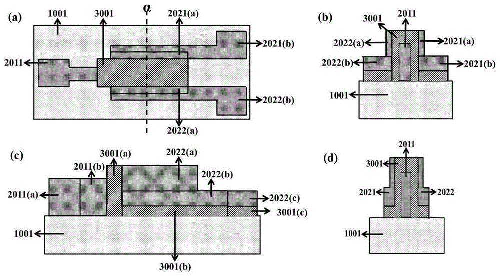
为此本发明的目的在于提供一种高密度铁电存储单元,采用一个存储单元中包含两个存储微单元的结构来提高存储密度,并且两个微单元共用一个下电极来减小微单元的体积,两个微单元中存储功能层不平行于衬底,下电极2011与存储功能层3001相接触的左侧面与衬底的夹角(φ)大于或者等于90°,同时下电极2011与存储功能层3001相接触的右侧面与衬底的夹角(θ)也大于或者等于90°。这种结构设计能够有效地提高衬底面积内铁电存储单位的数量,同时提高铁电存储单元的存储密度,这种铁电存储单元易于集成与三维堆垛,能有效地减小电极之间的相互影响,表面串扰问题,能促进高密度铁电存储器的应用。Therefore, the purpose of the present invention is to provide a high-density ferroelectric memory cell, which adopts a structure that includes two memory micro-units in one memory cell to improve the memory density, and the two micro-units share a lower electrode to reduce the micro-unit's Volume, the storage functional layer in the two micro-units is not parallel to the substrate, the angle ( φ ) between the left side of the
本发明采用以下技术方案:The present invention adopts following technical scheme:
一种高密度铁电存储器单元,包括衬底1001、下电极2011、存储功能层3001、左上电极2021、右上电极2022,所述的下电极2011与存储功能层3001相接触的左侧面与衬底的夹角(φ)大于或者等于90°,下电极2011与存储功能层3001相接触的右侧面与衬底的夹角(θ)也大于或者等于90°。A high-density ferroelectric memory cell includes a
所述衬底1001的材料为氧化铪、掺杂氧化铪、钛酸锶、铌掺杂钛酸锶、钛酸钡、氧化硅、掺杂氧化硅、氧化镁、氧化铝、钛酸钙、钛酸镁、白宝石、尖晶石、氧化钛、云母、石英、氧化铍、尖晶石、蓝宝石、砷化钾、红宝石、硅、铁酸钴、掺杂硅中的一种或者几种构成。The material of the
所述下电极2011为钌酸锶、掺杂钛酸锶、镧锶锰氧、掺铌钛酸锶、氧化铟锡、掺杂Si、氮化钛、铂、铌酸锂、掺杂铌酸锂中的一种或者几种构成。The
所述存储功能层3001为锆掺杂氧化铪、钇掺杂氧化铪、硅掺杂氧化铪、铝掺杂氧化铪、钆掺杂氧化铪、钛酸铅、钛酸锆铅、铁酸铋、掺杂铁酸铋、钛酸钡、掺杂钛酸钡、铁酸镥、掺杂铁酸镥、铁酸镓、掺杂铁酸镓中的一种或者几种构成,左上电极2021和下电极2011所夹持的部分存储功能层的厚度约为0.4nm-60nm,右上电极2022和下电极2011所夹持的部分存储功能层的厚度也约为0.4nm-60nm。The
所述存储功能层外延生长于衬底1001。The storage functional layer is epitaxially grown on the
所述下电极2011与左上电极2021及其所夹持的存储功能层3001部分可作为独立的一个存储微单元0001,下电极2011与右上电极2022及其所夹持的存储功能层3001部分可作为另外的一个存储微单元0002。The
所述下电极2011外接电路的部分延伸与存储单元的一侧,左上电极2021和右上电极2022外接电路的部分延伸于存储单元的另一侧。The part of the
所述的一种高密度铁电存储器单元内部包含的两个存储微单元0001和0002可存储表示的逻辑态数量相同,范围在2-16,并且两个存储微单元共用一个下电极2011,在存储态写入或者读取时下电极电势为零。The two storage micro-units 0001 and 0002 included in the high-density ferroelectric memory cell can store and represent the same number of logic states, ranging from 2 to 16, and the two storage micro-units share a
所述左上电极2021和右上电极2022可以为同种材料也可为不同种材料,可以为银、铜、含银合金、含铜合金、铂、铁、钴、镍、锌、钛、铝、掺杂硅、钌酸锶、掺杂钛酸锶、镧锶锰氧、掺铌钛酸锶、氧化铟锡、碳纳米管、石墨烯、掺杂石墨烯、二硫化钼、氮化钛、铂、铌酸锂、掺杂铌酸锂等金属或者半导体材料中的一种或者多种构成。The upper
本发明产生的有益效果:The beneficial effects that the present invention produces:
本发明中采用特殊形态的铁电薄膜使得同一铁电薄膜中两个不相互影响的部分能够分别用于存储,在一个新型高密度铁电存储单元中形成了两个存储微单元,并且两个存储微单元共用同一个下电极,极大地减小了存储微单元的体积,提高了存储单元的存储密度,见图1。另外,下电极2011外接电路的部分位于存储单元的一侧,左上电极2021和右上电极2022外接电路的部分位于存储单元的另一侧,极大地减小了三个电极之间的相互影响,提高了铁电存储单元性能存储性能的可靠性,见图1。特别需要注意的是,在该新型高密度铁电存储单元中利用存储功能层的极化来存储数据时,铁电薄膜的极化方向与衬底并不垂直,铁电薄膜极化方向的平行直线与衬底的夹角小于或者等于60°,下电极2011与存储功能层3001相接触的左侧面与衬底的夹角(φ)和存储功能层3001相接触的右侧面与衬底的夹角(θ)均大于或者等于90°(见图2),直接区别于传统的铁电存储器基于存储功能层垂直衬底的极化来存储数据的特点。该存储单元在实现存储时,可以在下电极2011和左上电极2021间施加电压使得存储功能层薄膜极化,在微单元0001中存储一个数值;类似的可以在下电极2011和右上电极2022间施加电压使得存储功能层薄膜极化,在微单元0002中存储一个数值。在读取微单元0001和微单元0002中的数值时,可在下电极2011和左上电极2021间施加一不会改变微单元0001存储态的电压来读取隧穿电流或者漏电流;可在下电极2011和右上电极2022间施加一不会改变微单元0002存储态的电压来读取隧穿电流或者漏电流;当微单元0001和微单元0002中的存储功能层的极化状态不同时,读取得到各自的隧穿电流或者漏电流值不同,从而可以识别微单元0001和微单元0002各自的存储状态。需要注意的是,微单元0001和微单元0002中的存储功能层在采用不同的写入方法写入时(以不同大小的脉冲电压为例,存储功能层的极化值可能不同,而不同的极化值会影响读取微单元0001和微单元0002时隧穿电流或者漏电流的大小,从而使得单个微单元实现多逻辑态存储的性能。这样能够进一步地提高存储器的存储容量和存储密度,具有广阔的应用前景。这种结构设计能够有效地提高衬底单位面积内铁电存储单位的数量,同时提高铁电存储单元的存储密度,易于集成,且适合三维堆垛,能促进高密度铁电存储器的应用。In the present invention, the special shape of the ferroelectric thin film is adopted, so that the two non-interacting parts in the same ferroelectric thin film can be respectively used for storage. The storage micro-units share the same lower electrode, which greatly reduces the volume of the storage micro-unit and improves the storage density of the storage unit, as shown in FIG. 1 . In addition, the part of the external circuit of the
附图说明Description of drawings
下面结合附图及实施方式对本发明作进一步详细的说明:Below in conjunction with accompanying drawing and embodiment, the present invention is described in further detail:
图1为一种高密度铁电存储器单元的(a)俯视图;(b)右视图;(c)主视图;(d)图1俯视图中α处的截面示意图。其中,2011a和2011b为下电极2011的部分;2021a和2021b为左上电极2021的部分;2022a、2022b和2022c是右上电极2022的部分;3001a、3001b和3001c是存储功能层3001的部分。FIG. 1 is (a) a top view of a high-density ferroelectric memory cell; (b) a right view; (c) a front view; (d) a schematic cross-sectional view at α in the top view of FIG. 1 . Among them, 2011a and 2011b are parts of the
图2为一种高密度铁电存储器单元制备过程中不同工艺程序后存储单元的(a)下电极刻蚀以后的俯视图;(b)下电极和存储功能层构成的异质结刻蚀以后的俯视图;(c)下电极和存储功能层构成的异质结刻蚀以后可选结构的俯视图;(d)下电极/存储功能层/上电极构成的异质结刻蚀以后的俯视图;(e)下电极/存储功能层/上电极构成的异质结刻蚀以后可选结构的俯视图。2 is a top view of (a) the lower electrode of the memory cell after different process procedures in the preparation process of a high-density ferroelectric memory cell; (b) the heterojunction composed of the lower electrode and the storage functional layer after etching Top view; (c) Top view of the optional structure after etching of the heterojunction composed of the lower electrode and the storage functional layer; (d) Top view of the heterojunction composed of the lower electrode/storage functional layer/upper electrode after etching; (e) ) The top view of the optional structure after the heterojunction composed of the lower electrode/storage functional layer/upper electrode is etched.
图3为一种高密度铁电存储器单元的(a)图1俯视图中α处的截面示意图中下电极左右侧面与衬底的夹角示意图;(b)图1俯视图中α处的截面示意图中下电极左右侧面与衬底的夹角不为90°时α处的截面示意图。3 is a schematic diagram of the angle between the left and right sides of the lower electrode and the substrate in (a) the schematic cross-sectional view at α in the top view of FIG. 1 of a high-density ferroelectric memory cell; (b) the schematic cross-sectional view at α in the top view of FIG. 1 A schematic cross-sectional view of the position at α when the angle between the left and right sides of the lower electrode and the substrate is not 90°.
具体实施方式Detailed ways
下面介绍的是本发明的多个可能实施例中的一些,旨在提供对本发明的基本了解,并不旨在确认本发明的关键或决定性的要素或限定所要保护的范围。The following descriptions of some of the many possible embodiments of the present invention are intended to provide a basic understanding of the invention, and are not intended to identify key or critical elements of the invention or to limit the scope of protection.
在附图中,为了清楚起见,夸大了层和区域的厚度,图示中的各部分之间的尺寸比例关系并不反映实际的尺寸比例关系。In the drawings, the thicknesses of layers and regions are exaggerated for the sake of clarity, and the dimensional proportions between parts in the drawings do not reflect the actual dimensional proportions.
实施例1Example 1
MoS2/BaTiO3/La0.66Sr0.33MnO3/SrTiO3一种新型高密度铁电存储器单元,其中衬底为SrTiO3,下电极为La0.66Sr0.33MnO3,存储功能层为BaTiO3,左上电极和右上电极均为MoS2,实现的主要流程:MoS 2 /BaTiO 3 /La 0.66 Sr 0.33 MnO 3 /SrTiO 3 is a new type of high-density ferroelectric memory cell, wherein the substrate is SrTiO 3 , the bottom electrode is La 0.66 Sr 0.33 MnO 3 , and the storage functional layer is BaTiO 3 , upper left The electrode and the upper right electrode are both MoS 2 , and the main process of realization is as follows:
a)将SrTiO3衬底上清洗干净并干燥。a ) Clean and dry the SrTiO3 substrate.
b)用脉冲激光分子束外延沉积技术在SrTiO3衬底上制备130nm厚的La0.66Sr0.33MnO3半导体下电极,构成La0.66Sr0.33MnO3/SrTiO3异质结。b) A 130nm-thick La 0.66 Sr 0.33 MnO 3 semiconductor lower electrode was fabricated on the SrTiO 3 substrate by pulsed laser molecular beam epitaxy to form a La 0.66 Sr 0.33 MnO 3 /SrTiO 3 heterojunction.
c)对La0.66Sr0.33MnO3/SrTiO3异质结刻蚀,其结构见图2(a),其中1001为衬底SrTiO3,2011为下电极La0.66Sr0.33MnO3,下电极垂直衬底方向的厚度为130nm左右,图1中下电极2011处2011a俯视时看到的形状,可选的可改为圆形或者菱形等。c) Etching La 0.66 Sr 0.33 MnO 3 /SrTiO 3 heterojunction, its structure is shown in Figure 2(a), where 1001 is the substrate SrTiO 3 , 2011 is the lower electrode La 0.66 Sr 0.33 MnO 3 , the lower electrode is vertically lined The thickness in the bottom direction is about 130 nm, and the shape of the
d)用脉冲激光分子束外延沉积技术在La0.66Sr0.33MnO3/SrTiO3异质结上制备4nm厚的BaTiO3铁电超薄膜,构成BaTiO3/La0.66Sr0.33MnO3/SrTiO3异质结,并再次刻蚀,其结构见图2(b),可选的其结构也可为图2(c)所示。d) A 4 nm-thick BaTiO3 ferroelectric ultra-thin film was prepared on the La 0.66 Sr 0.33 MnO 3 /SrTiO 3 heterojunction by pulsed laser molecular beam epitaxy, forming a BaTiO 3 /La 0.66 Sr 0.33 MnO 3 /SrTiO 3 heterojunction junction, and etched again, its structure is shown in Figure 2(b), and its optional structure can also be shown in Figure 2(c).
e)用化学气相沉积法制备MoS2二维材料半导体上电极,并使用机械剥离或者腐蚀转移的方法,将单层MoS2转移到BaTiO3铁电超薄膜上,构成MoS2/BaTiO3/La0.66Sr0.33MnO3/SrTiO3一种新型高密度铁电存储器单元,并进行刻蚀,其结构见图2(d)所示,可选的其结构可以为图2(e)所示。e) MoS 2 two-dimensional material semiconductor top electrode was prepared by chemical vapor deposition, and the single-layer MoS 2 was transferred to BaTiO 3 ferroelectric ultra-thin film by mechanical exfoliation or etching transfer method to form MoS 2 /BaTiO 3 /La 0.66 Sr 0.33 MnO 3 /SrTiO 3 is a new type of high-density ferroelectric memory cell, which is etched. Its structure is shown in Figure 2(d), and the optional structure can be shown in Figure 2(e).
(f)最终得到的基本单元结构俯视图见图1(a)所示,右视图见图1(b)所示,主视图见图1(c)所示,图1(a)处α截面的图如图1(d)所示。(f) The top view of the final basic unit structure is shown in Fig. 1(a), the right side view is shown in Fig. 1(b), and the front view is shown in Fig. 1(c). The figure is shown in Figure 1(d).
在该MoS2/BaTiO3/La0.66Sr0.33MnO3/SrTiO3一种新型高密度铁电存储器单元中,微单元0001中存储功能层BaTiO3的厚度为4nm左右,当存储功能层的极化指向左上电极时,其是一个存储状态,当存储功能层的极化指向下电极时,其是另一个存储状态。类似地,微单元0002中也是当存储功能层中的极化状态分别指向右上电极和下电极时,分别表示两个存储状态。在微单元0001和微单元0002中分别通过读取微单元中的隧穿电流来识别其中的存储状态。In the MoS 2 /BaTiO 3 /La 0.66 Sr 0.33 MnO 3 /SrTiO 3 a novel high-density ferroelectric memory cell, the thickness of the storage functional layer BaTiO 3 in the microcell 0001 is about 4 nm. When pointing to the upper left electrode, it is one storage state, and when the polarization of the storage functional layer points to the lower electrode, it is another storage state. Similarly, in the micro-unit 0002, when the polarization states in the storage functional layer point to the upper right electrode and the lower electrode, respectively, two storage states are represented respectively. In the micro-unit 0001 and the micro-unit 0002, respectively, the storage state in the micro-unit is identified by reading the tunneling current in the micro-unit.
实施例2Example 2
MoS2/BiFeO3/La0.66Sr0.33MnO3/SrTiO3一种新型高密度铁电存储器单元,其中衬底为SrTiO3,下电极为La0.66Sr0.33MnO3,存储功能层为BiFeO3且存储区域的厚度约为2nm,左上电极和右上电极均为MoS2,其实现方式与实施例1类似。MoS 2 /BiFeO 3 /La 0.66 Sr 0.33 MnO 3 /SrTiO 3 is a novel high-density ferroelectric memory cell, wherein the substrate is SrTiO 3 , the lower electrode is La 0.66 Sr 0.33 MnO 3 , the storage functional layer is BiFeO 3 and the memory The thickness of the region is about 2 nm, the upper left electrode and the upper right electrode are both MoS 2 , and the implementation is similar to that of Example 1.
在该MoS2/BiFeO3/La0.66Sr0.33MnO3/SrTiO3一种新型高密度铁电存储器单元中,微单元0001中存储功能层BiFeO3的厚度为2nm左右,当在左上电极和下电极间使用不同的操作电压在存储功能层中写入极化状态时,存储功能层的不同极化状态(极化值的大小、极化方向均可不同)表示存储单元的不同存储状态。类似地,微单元0002中也是当存储功能层中的不同极化状态表示微单元0002中的不同存储状态。分在微单元0001和微单元0002中分别通过读取微单元中的隧穿电流来识别其中的存储状态,并且均可以用作8逻辑态存储微单元来使用。In this MoS 2 /BiFeO 3 /La 0.66 Sr 0.33 MnO 3 /SrTiO 3 a new type of high-density ferroelectric memory cell, the thickness of the storage functional layer BiFeO 3 in the microcell 0001 is about 2nm, when the upper left electrode and the lower electrode When different operating voltages are used to write polarization states in the storage functional layer, the different polarization states of the storage functional layer (the magnitude of the polarization value and the polarization direction can be different) represent different storage states of the memory cell. Similarly, in microcell 0002 also different polarization states in the memory functional layer represent different storage states in microcell 0002. The micro-unit 0001 and the micro-unit 0002 are divided into the micro-unit 0001 and the micro-unit 0002 respectively to identify the storage state by reading the tunneling current in the micro-unit, and both can be used as 8 logic state storage micro-units.
实施例3Example 3
Pt/Si:HfO2/TiN/Si一种新型高密度铁电存储器单元,其中衬底为Si,下电极为TiN,存储功能层为Si:HfO2且存储区域的厚度约为3nm,左上电极和右上电极均为Pt,实现的主要流程:Pt/Si:HfO 2 /TiN/Si is a new type of high-density ferroelectric memory cell, in which the substrate is Si, the lower electrode is TiN, the storage functional layer is Si:HfO 2 and the thickness of the storage region is about 3nm, and the upper left electrode is and the upper right electrode are both Pt, the main process of realization:
a)将Si衬底上清洗干净并干燥。a) Clean and dry the Si substrate.
b)用原子层沉积系统技术在Si衬底上制备20nm厚的TiN半导体下电极,构成TiN/Si异质结。b) A 20nm-thick TiN semiconductor lower electrode was prepared on Si substrate by atomic layer deposition system technology to form a TiN/Si heterojunction.
c)对TiN/Si异质结刻蚀,其中1001为衬底SrTiO3,2011为下电极TiN,下电极垂直衬底方向的厚度为20nm左右。c) Etching the TiN/Si heterojunction, wherein 1001 is the substrate SrTiO 3 , 2011 is the lower electrode TiN, and the thickness of the lower electrode perpendicular to the substrate direction is about 20 nm.
d)用脉冲激光分子束外延沉积技术在TiN/Si异质结上制备4nm厚的Si:HfO2铁电超薄膜,构成Si:HfO2/TiN/Si异质结,并再次刻蚀。d) A 4 nm thick Si:HfO 2 ferroelectric ultra-thin film was prepared on the TiN/Si heterojunction by pulsed laser molecular beam epitaxy to form a Si:HfO 2 /TiN/Si heterojunction, and then etched again.
e)用小型离子溅射仪制备Pt上电极,并使用刻蚀方法,构成Pt/Si:HfO2/TiN/Si一种新型高密度铁电存储器单元,并进行刻蚀,得到的基本单元结构俯视图见图1(a)所示,右视图见图1(b)所示,主视图见图1(c)所示。e) Prepare the Pt upper electrode with a small ion sputtering apparatus, and use the etching method to form a new type of high-density ferroelectric memory cell of Pt/Si:HfO 2 /TiN/Si, and perform etching to obtain the basic cell structure The top view is shown in Figure 1(a), the right side view is shown in Figure 1(b), and the front view is shown in Figure 1(c).
在该Pt/Si:HfO2/TiN/Si一种新型高密度铁电存储器单元中,微单元0001中存储功能层Si:HfO2的厚度为3nm左右,当存储功能层的极化指向左上电极时,其是一个存储状态,当存储功能层的极化指向下电极时,其是另一个存储状态。类似地,微单元0002中也是当存储功能层中的极化状态分别指向右上电极和下电极时,分别表示两个存储状态。在微单元0001和微单元0002中分别通过读取微单元中的隧穿电流来识别其中的存储状态。In this new type of high-density ferroelectric memory cell of Pt/Si:HfO 2 /TiN/Si, the thickness of the memory functional layer Si:HfO 2 in the micro-unit 0001 is about 3 nm. When the polarization of the memory functional layer points to the upper left electrode , it is one storage state, and when the polarization of the storage functional layer points to the lower electrode, it is another storage state. Similarly, in the micro-unit 0002, when the polarization states in the storage functional layer point to the upper right electrode and the lower electrode, respectively, two storage states are represented respectively. In the micro-unit 0001 and the micro-unit 0002, respectively, the storage state in the micro-unit is identified by reading the tunneling current in the micro-unit.
实施例4Example 4
Au/Si:HfO2/TiN/Si一种新型高密度铁电存储器单元,其中衬底为Si,下电极为TiN,存储功能层为Si:HfO2且存储区域的厚度约为3nm,左上电极和右上电极均为Au,其实现方式与实施例3类似,不同之处为其左右上电极为Au。Au/Si:HfO 2 /TiN/Si is a new type of high-density ferroelectric memory cell, in which the substrate is Si, the lower electrode is TiN, the storage functional layer is Si:HfO 2 and the thickness of the storage region is about 3nm, and the upper left electrode is The upper and right electrodes are both Au, and the implementation is similar to that in Example 3, except that the left and right upper electrodes are Au.
在该Pt/Si:HfO2/TiN/Si一种新型高密度铁电存储器单元中,微单元0001中存储功能层Si:HfO2的厚度为3nm左右,当存储功能层的极化指向左上电极时,其是一个存储状态,当存储功能层的极化指向下电极时,其是另一个存储状态。类似地,微单元0002中也是当存储功能层中的极化状态分别指向右上电极和下电极时,分别表示两个存储状态。在微单元0001和微单元0002中分别通过读取微单元中的隧穿电流来识别其中的存储状态。In this new type of high-density ferroelectric memory cell of Pt/Si:HfO 2 /TiN/Si, the thickness of the memory functional layer Si:HfO 2 in the micro-unit 0001 is about 3 nm. When the polarization of the memory functional layer points to the upper left electrode , it is one storage state, and when the polarization of the storage functional layer points to the lower electrode, it is another storage state. Similarly, in the micro-unit 0002, when the polarization states in the storage functional layer point to the upper right electrode and the lower electrode, respectively, two storage states are represented respectively. In the micro-unit 0001 and the micro-unit 0002, respectively, the storage state in the micro-unit is identified by reading the tunneling current in the micro-unit.
实施例5Example 5
Graphene/BiFeO3/La0.66Sr0.33MnO3/SrTiO3一种新型高密度铁电存储器单元,其中衬底为SrTiO3,下电极为La0.66Sr0.33MnO3,存储功能层为BiFeO3且存储区域的厚度约为2nm,左上电极和右上电极均为Graphene,其实现方式与实施例1类似。Graphene/BiFeO 3 /La 0.66 Sr 0.33 MnO 3 /SrTiO 3 is a novel high-density ferroelectric memory cell, wherein the substrate is SrTiO 3 , the lower electrode is La 0.66 Sr 0.33 MnO 3 , the storage functional layer is BiFeO 3 and the storage region is The thickness is about 2 nm, the upper left electrode and the upper right electrode are both Graphene, and the implementation is similar to that in Example 1.
在该Graphene/BiFeO3/La0.66Sr0.33MnO3/SrTiO3一种新型高密度铁电存储器单元中,微单元0001中存储功能层BiFeO3的厚度为2nm左右,当在左上电极和下电极间使用不同的操作电压在存储功能层中写入极化状态时,存储功能层的不同极化状态(极化值的大小、极化方向均可不同)表示存储单元的不同存储状态。类似地,微单元0002中也是当存储功能层中的不同极化状态表示微单元0002中的不同存储状态。在微单元0001和微单元0002中分别通过读取微单元中的隧穿电流来识别其中的存储状态,并且均可以用作8逻辑态存储微单元来使用。In the Graphene/BiFeO 3 /La 0.66 Sr 0.33 MnO 3 /SrTiO 3 , a new type of high-density ferroelectric memory cell, the thickness of the storage functional layer BiFeO 3 in the micro-unit 0001 is about 2 nm. When different operating voltages are used to write polarization states in the storage functional layer, different polarization states of the storage functional layer (the magnitude of the polarization value and the polarization direction can be different) represent different storage states of the memory cell. Similarly, in microcell 0002 also different polarization states in the memory functional layer represent different storage states in microcell 0002. In the micro-unit 0001 and the micro-unit 0002, respectively, the memory states in the micro-units are identified by reading the tunneling current in the micro-units, and both can be used as 8 logic-state memory micro-units.
实施例6Example 6
Graphene/BiFeO3/La0.66Sr0.33MnO3/SrTiO3一种新型高密度铁电存储器单元,其中衬底为SrTiO3,下电极为La0.66Sr0.33MnO3,存储功能层为BiFeO3且存储区域的厚度约为20nm,左上电极和右上电极均为Graphene,其实现方式与实施例1类似。Graphene/BiFeO 3 /La 0.66 Sr 0.33 MnO 3 /SrTiO 3 is a novel high-density ferroelectric memory cell, wherein the substrate is SrTiO 3 , the lower electrode is La 0.66 Sr 0.33 MnO 3 , the storage functional layer is BiFeO 3 and the storage area is The thickness of the electrode is about 20 nm, and the upper left electrode and the upper right electrode are both Graphene, and the realization method is similar to that of Example 1.
在该Graphene/BiFeO3/La0.66Sr0.33MnO3/SrTiO3一种新型高密度铁电存储器单元中,微单元0001中存储功能层BiFeO3的厚度为20nm左右,当在左上电极和下电极间使用不同的操作电压在存储功能层中写入极化状态时,存储功能层的不同极化状态(极化值的大小、极化方向均可不同)表示存储单元的不同存储状态。类似地,微单元0002中也是当存储功能层中的不同极化状态表示微单元0002中的不同存储状态。在微单元0001和微单元0002中存储功能层中具有较多的氧空位,分别通过读取微单元中的漏电流来识别其中的存储状态,并且均可以用作16逻辑态存储微单元来使用。In the Graphene/BiFeO 3 /La 0.66 Sr 0.33 MnO 3 /SrTiO 3 a new type of high-density ferroelectric memory cell, the thickness of the storage functional layer BiFeO 3 in the micro-unit 0001 is about 20 nm, when the thickness between the upper left electrode and the lower electrode is about 20 nm. When different operating voltages are used to write polarization states in the storage functional layer, different polarization states of the storage functional layer (the magnitude of the polarization value and the polarization direction can be different) represent different storage states of the memory cell. Similarly, in microcell 0002 also different polarization states in the memory functional layer represent different storage states in microcell 0002. There are many oxygen vacancies in the storage functional layer in the micro-unit 0001 and the micro-unit 0002. The storage states in the micro-units can be identified by reading the leakage current in the micro-units, and both can be used as 16 logic-state storage micro-units. .
实施例7Example 7
Ag/PbZr0.52Ti0.48O3/Pt/SrTiO3一种新型高密度铁电存储器单元,其中衬底为SrTiO3,下电极为Pt,存储功能层为BiFeO3且存储区域的厚度约为20nm,左上电极和右上电极均为Ag,其实现方式与实施例1类似。Ag/PbZr 0.52 Ti 0.48 O 3 /Pt/SrTiO 3 is a new type of high-density ferroelectric memory cell, in which the substrate is SrTiO 3 , the lower electrode is Pt, the storage functional layer is BiFeO 3 and the thickness of the storage region is about 20nm, The upper left electrode and the upper right electrode are both Ag, and the realization method is similar to that of Example 1.
在该Ag/PbZr0.52Ti0.48O3/Pt/SrTiO3一种新型高密度铁电存储器单元中,微单元0001中存储功能层PbZr0.52Ti0.48O3的厚度为20nm左右,当在左上电极和下电极间使用不同的操作电压在存储功能层中写入极化状态时,存储功能层的不同极化状态(极化值的大小、极化方向均可不同)表示存储单元的不同存储状态,同时在电压作用下Ag电极与PbZr0.52Ti0.48O3界面处会生成AgO x 或者分解AgO x 来调控PbZr0.52Ti0.48O3内部的氧空位,致使两个微单元中的开关比大幅度地提高。类似地,微单元0002中也是当存储功能层中的不同极化状态表示微单元0002中的不同存储状态,也存在电压作用下Ag电极与PbZr0.52Ti0.48O3界面处会生成AgO x 或者分解AgO x 来调控PbZr0.52Ti0.48O3内部的氧空位。在微单元0001和微单元0002中存储功能层中分别通过读取微单元中的漏电流来识别其中的存储状态,并且均可以用作6逻辑态存储微单元来使用。In the Ag/PbZr 0.52 Ti 0.48 O 3 /Pt/SrTiO 3 a new type of high-density ferroelectric memory cell, the thickness of the storage functional layer PbZr 0.52 Ti 0.48 O 3 in the micro-unit 0001 is about 20 nm. When the upper left electrode and the When different operating voltages are used between the lower electrodes to write the polarization states in the storage functional layer, the different polarization states of the storage functional layer (the magnitude of the polarization value and the polarization direction can be different) represent the different storage states of the memory cells. At the same time, under the action of voltage, AgO x will be generated at the interface between Ag electrode and PbZr 0.52 Ti 0.48 O 3 or AgO x will be decomposed to regulate the oxygen vacancies inside PbZr 0.52 Ti 0.48 O 3 , resulting in a significant increase in the on-off ratio of the two microcells. . Similarly, in the micro-unit 0002, when the different polarization states in the storage functional layer represent different storage states in the micro-unit 0002, there is also AgO x or decomposition at the interface between the Ag electrode and the PbZr 0.52 Ti 0.48 O 3 under the action of voltage. AgO x to modulate the oxygen vacancies inside PbZr 0.52 Ti 0.48 O 3 . In the storage function layer of the micro-unit 0001 and the micro-unit 0002, the storage state in the micro-unit is identified by reading the leakage current in the micro-unit, and both can be used as a 6-logic state storage micro-unit.
实施例8Example 8
MoS2/BaTiO3/La0.66Sr0.33MnO3/SrTiO3一种新型高密度铁电存储器单元,其中衬底为SrTiO3,下电极为La0.66Sr0.33MnO3,存储功能层为BaTiO3,左上电极和右上电极均为MoS2,其实现方式与实施例1类似,不同之处为其图1俯视图中α处的截面的下电极左右侧面与衬底的夹角不为90读,示意图如图3(a)所示,图3(b)为图1俯视图中α处的截面示意图中下电极左右侧面与衬底的夹角不为90°时α处的截面示意图。MoS 2 /BaTiO 3 /La 0.66 Sr 0.33 MnO 3 /SrTiO 3 is a new type of high-density ferroelectric memory cell, wherein the substrate is SrTiO 3 , the bottom electrode is La 0.66 Sr 0.33 MnO 3 , and the storage functional layer is BaTiO 3 , upper left The electrode and the upper right electrode are both MoS 2 , and the implementation method is similar to that of Example 1, except that the angle between the left and right sides of the lower electrode and the substrate of the section at α in the top view of FIG. 1 is not 90°, as shown in the schematic diagram. 3(a), FIG. 3(b) is a schematic cross-sectional view at α when the angle between the left and right sides of the lower electrode and the substrate is not 90° in the schematic cross-sectional view at α in the top view of FIG. 1 .
Claims (7)
Priority Applications (1)
| Application Number | Priority Date | Filing Date | Title |
|---|---|---|---|
| CN201810597386.7A CN108520879B (en) | 2018-06-12 | 2018-06-12 | High-density ferroelectric memory unit |
Applications Claiming Priority (1)
| Application Number | Priority Date | Filing Date | Title |
|---|---|---|---|
| CN201810597386.7A CN108520879B (en) | 2018-06-12 | 2018-06-12 | High-density ferroelectric memory unit |
Publications (2)
| Publication Number | Publication Date |
|---|---|
| CN108520879A CN108520879A (en) | 2018-09-11 |
| CN108520879B true CN108520879B (en) | 2020-09-29 |
Family
ID=63428288
Family Applications (1)
| Application Number | Title | Priority Date | Filing Date |
|---|---|---|---|
| CN201810597386.7A Active CN108520879B (en) | 2018-06-12 | 2018-06-12 | High-density ferroelectric memory unit |
Country Status (1)
| Country | Link |
|---|---|
| CN (1) | CN108520879B (en) |
Families Citing this family (2)
| Publication number | Priority date | Publication date | Assignee | Title |
|---|---|---|---|---|
| CN109378313B (en) * | 2018-09-23 | 2020-10-30 | 复旦大学 | A low-power three-dimensional non-volatile memory and preparation method thereof |
| WO2021163963A1 (en) * | 2020-02-20 | 2021-08-26 | 华为技术有限公司 | Ferroelectric memory and electronic device |
Citations (5)
| Publication number | Priority date | Publication date | Assignee | Title |
|---|---|---|---|---|
| CN101038951A (en) * | 2006-03-15 | 2007-09-19 | 旺宏电子股份有限公司 | Manufacturing method of tubular electrode phase change memory |
| CN101101961A (en) * | 2007-07-17 | 2008-01-09 | 中国科学院上海微系统与信息技术研究所 | Phase change memory device unit with annular phase change material and preparation method |
| CN101237026A (en) * | 2007-01-31 | 2008-08-06 | 旺宏电子股份有限公司 | Memory cell with side electrode |
| CN101271862A (en) * | 2007-03-19 | 2008-09-24 | 财团法人工业技术研究院 | Memory element and its manufacturing method |
| CN103427016A (en) * | 2013-08-29 | 2013-12-04 | 湘潭大学 | Piezoelectric memorizer unit based on ferroelectric tunnel junctions and manufacturing method thereof |
-
2018
- 2018-06-12 CN CN201810597386.7A patent/CN108520879B/en active Active
Patent Citations (5)
| Publication number | Priority date | Publication date | Assignee | Title |
|---|---|---|---|---|
| CN101038951A (en) * | 2006-03-15 | 2007-09-19 | 旺宏电子股份有限公司 | Manufacturing method of tubular electrode phase change memory |
| CN101237026A (en) * | 2007-01-31 | 2008-08-06 | 旺宏电子股份有限公司 | Memory cell with side electrode |
| CN101271862A (en) * | 2007-03-19 | 2008-09-24 | 财团法人工业技术研究院 | Memory element and its manufacturing method |
| CN101101961A (en) * | 2007-07-17 | 2008-01-09 | 中国科学院上海微系统与信息技术研究所 | Phase change memory device unit with annular phase change material and preparation method |
| CN103427016A (en) * | 2013-08-29 | 2013-12-04 | 湘潭大学 | Piezoelectric memorizer unit based on ferroelectric tunnel junctions and manufacturing method thereof |
Also Published As
| Publication number | Publication date |
|---|---|
| CN108520879A (en) | 2018-09-11 |
Similar Documents
| Publication | Publication Date | Title |
|---|---|---|
| CN102282673A (en) | Transparent memory for transparent electronic device | |
| CN108538920B (en) | Flexible ferroelectric thin film transistor and preparation method thereof | |
| Gayakvad et al. | Spinel ferrites for resistive random access memory applications | |
| JP2006179891A (en) | Voltage controlled magnetization reversal recording type MRAM element and information recording and reading method using the same | |
| CN102439724A (en) | Ferro-resistive random access memory (ferro-rram), operation method and manufacturing mehtod thereof | |
| CN110061056B (en) | Novel ferroelectric field effect transistor unit and writing and reading method thereof | |
| CN111755447B (en) | A high-density ferroelectric memory cell based on multiple logic states and its regulation method | |
| CN108520879B (en) | High-density ferroelectric memory unit | |
| CN115666133A (en) | Capacitanceless DRAM based on oxide two-dimensional electron gas transistor and its preparation method | |
| Lei et al. | Nonvolatile and volatile resistive switching characteristics in MoS2 thin film for RRAM application | |
| CN108550551B (en) | Non-destructive read ferroelectric multi-logic state memory cell and write/read/erase operation method for storing data based on domain wall density | |
| CN108389962B (en) | In-plane read/write ferrous resistance variable memory and method for enhancing read/write signal | |
| Long et al. | Competing ferroelectric polarization and defect migration induced resistive switching in β′-In2Se3 | |
| US12080783B2 (en) | Spin transistors based on voltage-controlled magnon transport in multiferroic antiferromagnets | |
| CN108469315B (en) | Pressure sensor unit based on electric conductivity of oxygen vacancy electron gas of ferroelectric domain wall | |
| TW201203551A (en) | Field effect transistor and memory device | |
| CN207398179U (en) | A kind of magnetoelectricity Memory Storage Unit structure | |
| CN114725124A (en) | A kind of semiconductor structure based on ferroelectric Schottky tunneling junction and preparation method thereof | |
| CN111732128A (en) | Two-dimensional tetragonal ferromagnetic material and preparation method thereof, storage unit and method for regulating storage unit to identify and store data | |
| CN119677396A (en) | A multiferroic tunnel junction, device and method based on Janus ferroelectric material | |
| JP2006210525A (en) | Memory element and circuit element | |
| CN113224232B (en) | SOT-MRAM based on bottom electrode vertical voltage control and manufacturing and writing methods | |
| WO2023236361A1 (en) | Semiconductor structure and memory | |
| Wei et al. | Dielectric properties and ferroelectric resistive switching mechanism in the epitaxial (111) BiFeO3 films | |
| CN119136559B (en) | A ferroelectric tunnel junction memory device |
Legal Events
| Date | Code | Title | Description |
|---|---|---|---|
| PB01 | Publication | ||
| PB01 | Publication | ||
| SE01 | Entry into force of request for substantive examination | ||
| SE01 | Entry into force of request for substantive examination | ||
| GR01 | Patent grant | ||
| GR01 | Patent grant |