Detailed Description
Hereinafter, embodiments of the present invention capable of achieving the above objects will be described with reference to the accompanying drawings.
In the description of the embodiments according to the present invention, in the case where it is described as being formed "above or below" each element, all of the above or below causes two elements to be directly contacted with each other or one or more other elements to be indirectly formed between the two elements. Further, when it is expressed as "above or below", it may include not only an upward direction but also a downward direction based on the element.
It will be further understood that the terms "first" and "second," "upper/over" and "lower/under" may be used solely to distinguish one entity or element from another entity or element without necessarily requiring or implying any physical relationship or sequence.
The thickness and size of each layer in the drawings are exaggerated, omitted, or schematically shown for convenience and clarity of explanation. Moreover, the size of each component does not fully reflect the actual size.
The phosphor composition of the present embodiment includes a cyan phosphor excited by an excitation light source to emit light of a first wavelength region of cyan, a green phosphor excited by the excitation light source to emit light of a second wavelength region of green, and a red phosphor to emit red light of a third wavelength region of red. The excitation light source may be blue, but is not limited thereto as long as it does not depart from the object of the present invention. Fig. 1 is a view showing the emission wavelength and excitation wavelength of a blue-green phosphor.
As shown, the excitation wavelength of the cyan phosphor may include blue light of 350nm (nanometers) to 450nm, and the emission wavelength may have a peak of 490nm to 505nm, for example, a peak of 498 nm.
The half width of light emitted from the blue-green phosphor may be about 32 nanometers, and may include phosphor particles having different diameters. For example, the size of phosphor particles having a size corresponding to 10% of the whole is 12.1 mm. The size of the phosphor particles having a size within 50% of the whole may be 17.6 mm, and the size of the phosphor particles having a size within 90% of the whole may be 27.0 mm.
The first phosphor can be represented by the formula (Ba, Mg)3-aSi6-bO3.5-cN8.5-d(Li,Cl,F,P)1-e:Eu2+ aWherein a is more than or equal to 0.01 and less than or equal to 0.30, b is more than or equal to 0.01 and less than or equal to 1.0, c is more than or equal to 0.01 and less than or equal to 0.5, d is more than or equal to 0.01 and less than or equal to 0.5, and e is more than or equal to 0.01 and less than or equal to 0.9. Alternatively, the first phosphor may be represented by the formula (Ba, Mg, Ca, Sr)3-fSi6O3N8:Eu2+ fWherein f is 0.01-0.30. Alternatively, the first phosphor may be represented by the formula (Ba, Mg, Ca, Sr)1-gSi2O2N2:Eu2+ gWherein 0.01. ltoreq. g.ltoreq.0.30.
The second phosphor can be represented by the formula (Lu, Y, Gd)3-h(Al,Ga)5O12:Ce3+ hA LuAG-based phosphor or a YAG-based phosphor represented by (1) wherein 0.01. ltoreq. h.ltoreq.0.50. Alternatively, the second phosphor may be represented by the formula La3-iSi6N11:Ce3+ iWherein i is 0.01. ltoreq. i.ltoreq.0.50.
The third phosphor can be represented by the formula (Ca, Sr)1-jAlSiN3:Eu2+ jWherein j is 0.01. ltoreq. j.ltoreq.0.30. Alternatively, the third phosphor may be composed of Sr2-kSi5N8:Eu2+ kAnd 0.01. ltoreq. k.ltoreq.0.30. Alternatively, the third phosphor may be composed of (Ba, Sr)2-lSi5N8:Eu2+ lAnd can be 0.01. ltoreq. 1. ltoreq.0.30.
Fig. 2a to 2c are views showing the intensity of light according to the wavelength of the blue-green phosphor, the green phosphor, and the red phosphor contained in the phosphor composition.
In fig. 2a, the emission peak wavelength of the first phosphor emits light in a blue green wavelength range of 490nm to 505nm, the emission peak wavelength of the second phosphor in fig. 2b emits light in a green wavelength range of 515nm to 575nm, the emission peak wavelength of the third phosphor emits light in a red wavelength range of 580nm to 670nm, and the wavelength range and intensity of the emitted light may vary with the composition of the first to third phosphors.
Fig. 3 is a view illustrating an embodiment of a light emitting device package 200.
The light emitting device package 200 according to the embodiment may include a body 210, a cavity formed on the body 210, and the light emitting device 100 disposed in the cavity. And the light emitting device package 200 may include lead frames 221 and 222 for electrical connection with the printed circuit board 100. The light emitting device 100 may be disposed on a bottom surface of the cavity among the cavities, and the molding part 260 may be disposed on the cavity surrounding the light emitting device 100.
The molding part 260 may include the phosphor composition of the above embodiment.
The body 210 may be formed of a silicone material, a synthetic resin material, or a metal material. The body 210 may include a cavity having an open top surface and side and bottom surfaces.
The cavity may be formed in a cup shape, a concave container shape, or the like, and a side surface of the cavity may be formed perpendicularly or obliquely with respect to the bottom surface, and may vary in size and shape.
The shape of the cavity viewed from above may be a circle, a polygon, an ellipse, etc., and it may be a shape having a curved edge, but the present invention is not limited thereto.
The body 210 may include a first lead frame 221 and a second lead frame 222 to be electrically connected to the light emitting device 100. When the body portion 210 is made of a conductive type material such as a metal material, although not shown, an insulating layer is coated on a surface of the body portion 210 to prevent an electrical short between the first and second lead frames 221 and 222.
The first and second lead frames 221 and 222 are electrically separated from each other and may supply current to the light emitting device 100. The first and second lead frames 221 and 222 may reflect light 100 generated from the light emitting device to increase light efficiency and may radiate heat generated from the light emitting device 100 to the outside to dissipate heat.
The light emitting device 100 may be disposed in the cavity and on the body 210 or on the first lead frame 221 or the second lead frame 222. The light emitting device 100 to be disposed may be a vertical light emitting device, a horizontal lamp light emitting device, or the like.
In fig. 3, the light emitting device 100 may be disposed on the first lead frame 221 and the second lead frame 222 may be connected to the light emitting device 100 through the wire 250. However, the light emitting device 100 may be connected to the lead frame by a flip chip bonding or die bonding method in addition to the wire bonding method.
In the light emitting device package 200 of fig. 3, the molding part 260 protects the light emitting device 100 and fills the inside of the cavity.
Further, the molding part 260 may be formed to include the phosphor composition and the resin of the embodiment having the plurality of phosphors 262, 264, and 266.
The molding part 260 may include resin and phosphors 262, 264, and 266, and may be disposed to surround the light emitting device 100 to protect the light emitting device 100.
The resin that can be mixed and used with the phosphor composition in the molding portion 260 may be any one of a silicone resin, an epoxy resin, and an acrylic resin, or a mixture thereof.
The phosphors 262, 264 and 266 are excited by light emitted from the light emitting device 100 to emit wavelength-converted light. The phosphors 262, 264 and 266 may correspond to the first phosphor, the second phosphor and the third phosphor, respectively.
Although not shown in the drawings, the molding 260 may be arranged in a dome shape filling the cavity and higher than the height of the side of the cavity. In order to adjust the light output angle of the light emitting device package 200, the molding part 260 may be arranged in a dome shape. The molding part may surround and protect the light emitting device 100 and serve as a lens for changing a path of light emitted from the light emitting device 100. Fig. 4 shows an embodiment of a light emitting device 100. The light emitting device 100 includes a support substrate 170, a light emitting structure 120, an ohmic layer 140, and a first electrode 180.
The light emitting structure 120 may include a first conductive type semiconductor layer 122, an active layer 124, and a second conductive type semiconductor layer 126.
The first conductive type semiconductor layer 122 may be formed of a compound semiconductor such as group III-V or group II-VI, and may be doped with a first conductive type dopant. The first conductive type semiconductor layer 122 is of AlxInyGa(1-x-y)N (0. ltoreq. x.ltoreq.1, 0. ltoreq. y.ltoreq.1, 0. ltoreq. x + y. ltoreq.1), for example, any of AlGaN, GaN, InAlGaAs, GaP, GaAs, GaAsP, and AlGaInP.
When the first conductive type semiconductor layer 122 is an n-type semiconductor layer, the first conductive type dopants may include n-type dopants such as Si, Ge, Sn, Se, and Te. The first conductive type semiconductor layer 122 may be formed as a single layer or a plurality of layers, but the present invention is not limited thereto.
The active layer 124 may be disposed between the first conductive type semiconductor layer 122 and the second conductive type semiconductor layer 126, and may include a single well structure, a multi-well structure, a single quantum well structure, a Multiple Quantum Well (MQW) structure, a quantum dot structure, or a quantum wire structure.
The active layer may be formed of a compound semiconductor material such as group III-V. The active layer may be a pair structure having a well layer and a barrier layer, such as one of AlGaN/AlGaN, InGaN/GaN, InGaN/InGaN, AlGaN/GaN, InAlGaN/GaN, GaAs (InGaAs)/AlGaAs, GaP (InGaP)/AlGaP, but is not limited thereto. The well layer may be formed of a material having an energy bandgap smaller than that of the barrier layer.
The second conductive type semiconductor layer 126 may be formed of a semiconductor compound. The second conductive type semiconductor layer 126 may be formed of a compound semiconductor such as group III-V or group II-VI, and may be doped with a second conductive type dopant. The second conductive type semiconductor layer 126 may be of InxAlyGa1-x-yN (0. ltoreq. x.ltoreq.1, 0. ltoreq. y.ltoreq.1, 0. ltoreq. x + y. ltoreq.1), e.g. AlGaN, GaN AlInN, AlGaAs, GaP, GaAs, GaAsP, AlGOne of aInP. For example, the second conductive type semiconductor layer 126 may be made of AlxGa(1-x)And N is formed.
When the second conductive type semiconductor layer 126 is a p-type semiconductor layer, the second conductive type dopant may be a p-type dopant such as Mg, Zn, Ca, Sr, or Ba. The second conductive type semiconductor layer 126 may be formed as a single layer or a plurality of layers, but the present invention is not limited thereto.
The surface of the first conductive type semiconductor layer 122 has a pattern, and light extraction efficiency may be improved. The first electrode 180 may be disposed on a surface of the first conductive type semiconductor layer 122, and may be disposed on a surface of the first conductive type semiconductor layer 122 on which the first electrode 180 is disposed, without a pattern. The first electrode 180 may be formed in a single layer or a multi-layer structure including at least one of aluminum (Al), titanium (Ti), chromium (Cr), nickel (Ni), and copper (Cu).
The passivation layer 190 may be formed around the light emitting structure 120. The passivation layer 190 may be made of an insulating material, and the insulating material may be made of a non-conductive oxide or nitride. For example, the passivation layer 190 may include silicon oxide (SiO)2) A layer, an oxynitride layer, and an aluminum oxide layer.
A second electrode may be disposed under the light emitting structure 120, and the ohmic layer 140 and the reflective layer 150 may serve as the second electrode. GaN may be disposed under the second conductive type semiconductor layer 126 so that current or holes may be smoothly supplied to the second conductive type semiconductor layer 126.
Ohmic layer 140 may have a thickness of about 200 angstroms
Is measured. The
ohmic layer 140 may be formed of Indium Tin Oxide (ITO), Indium Zinc Oxide (IZO), Indium Zinc Tin Oxide (IZTO), Indium Aluminum Zinc Oxide (IAZO), Indium Gallium Zinc Oxide (IGZO), indium gallium tin oxide, AZO (aluminum zinc oxide), ATO (antimony tin oxide), GZO (gallium zinc oxide), IZON (IZO nitride), AGZO (Al-GaZnO), IGZO, NiO, RuOx/ITO, Ni/IrOx/Au, and Ni/IrOx/Au/ITO, Ag, Ni, Cr, Ti, Al, Rh, Pd, Sn, In, Ru, Au, and Hf, and the present invention is applicable to Indium Tin Oxide (ITO), Indium Gallium Zinc Oxide (IGZO), indium gallium tin oxide (IZOThe invention is not limited to these materials.
The reflective layer 150 may be formed of a metal layer such as molybdenum (Mo), aluminum (Al), silver (Ag), nickel (Ni), platinum (Pt), rhodium (Rh), or a composite material including Al, Ag, Pt, or Rh. The reflective layer 150 effectively reflects light generated in the active layer 124, thereby greatly improving light extraction efficiency of the semiconductor device.
The support substrate 170 may be formed of a conductive material such as a metal or a semiconductor material. A metal having excellent electrical or thermal conductivity may be used as the support substrate 170, and a material having high thermal conductivity (e.g., a metal, etc.) may be used to radiate heat generated by the operating light emitting device. For example, the support substrate 170 may be selected from the group consisting of molybdenum (Mo), silicon (Si), tungsten (W), copper (Cu), and aluminum (Al) or an alloy thereof, and gold (Au), a copper alloy (Cu alloy), nickel (Ni), copper-tungsten (Cu-W), a carrier wafer (e.g., GaN, Si, Ge, GaAs, ZnO, SiGe, SiC, SiGe, and Ga)2O3Any of the above) is used.
The support substrate 170 may have a thickness ranging from 50 to 200 μm so as to have sufficient mechanical strength to be separated into individual chips through the scribing process and the breaking process without causing warpage of the entire nitride semiconductor.
The bonding layer 160 couples the reflective layer 150 and the support substrate 170 and may be formed of gold (Au), tin (Sn), indium (In), aluminum (Al), silicon (Si), silver (Ag), nickel (Ni), and copper (Cu), or an alloy thereof.
The embodiment of the light emitting device 100 shown in fig. 4 is an embodiment of a vertical light emitting device. In the embodiment of the light emitting device package 200 shown in fig. 3, a light emitting device and a flip-chip type light emitting device may be arranged in addition to the vertical light emitting device shown in fig. 4. In this case, the light emitting device 100 may emit light in a blue wavelength range.
The embodiment of the light emitting device package of fig. 4 including the light emitting device of one embodiment shown in fig. 3 may emit white light.
In the first embodiment of the phosphor composition, the weight ratio of the first phosphor may be 1 wt% to 15 wt%, the weight ratio of the second phosphor may be 75 wt% to 90 wt%, and the weight ratio of the third phosphor may be 2 wt% to 15 wt%. The phosphor may be contained in the molding part of the light emitting device package at a weight ratio of 10 wt% to 30 wt%. In detail, the weight ratio of the first phosphor may be present in a range of 5 wt% to 9 wt%, the weight ratio of the second phosphor may be 82 wt% to 90 wt%, and the weight ratio of the third phosphor may be 4 wt% to 8 wt%. The phosphor may be contained in a weight ratio of 10 wt% to 18 wt%.
Table 1 and table 2 show characteristics of light emitted from the light emitting device package including the phosphor composition according to the comparative example and the first embodiment, respectively, when the color temperature of light emitted from the light emitting device package is 6500K (absolute temperature scale).
[ TABLE 1]
| |
lm
|
Cx
|
Cy
|
CCT
|
CRI
|
R9
|
| Minimum size
|
6.07
|
0.312
|
0.322
|
6316
|
83.4
|
8
|
| Maximum of
|
6.21
|
0.316
|
0.329
|
6613
|
85.0
|
17
|
| Average
|
6.13
|
0.314
|
0.325
|
6451
|
84.1
|
13 |
[ TABLE 2 ]
| |
lm
|
Cx
|
Cy
|
CCT
|
CRI
|
R9
|
| Minimum size
|
5.47
|
0.312
|
0.322
|
6308
|
89.0
|
50
|
| Maximum of
|
5.65
|
0.316
|
0.329
|
6622
|
92.5
|
68
|
| Average
|
5.57
|
0.314
|
0.325
|
6450
|
90.7
|
58 |
Fig. 5a to 5c show the optical characteristics of the first embodiment of the phosphor composition at this time together with a comparative example. In fig. 5a, the horizontal axis represents Cx value and the vertical axis represents Cy value. In fig. 5b, the ordinate represents illuminance (lm), the abscissa represents the value of Cy, and in fig. 5c, the abscissa represents wavelength and the ordinate represents intensity (W).
In the comparative example, the green phosphor may be included at 85 wt% to 95 wt%, and the red phosphor may be included at 5 wt% to 15 wt%. The phosphor may be contained in the molding part of the light emitting device package at a weight ratio of 10 wt% to 30 wt%.
The Color Rendering Index (CRI) and the color rendering index (R9) of the red region of the light emitting device package of the phosphor composition according to the first embodiment shown in table 2 were improved and the Correlated Color Temperature (CCT) was similar, as compared to those of the light emitting device package (CRT) and R9 according to the comparative example shown in table 1.
In the second and third embodiments of the phosphor composition, the weight ratio of the first phosphor is 1 wt% to 15 wt%, the weight ratio of the second phosphor is 75 wt% to 90 wt%, and the weight ratio of the third phosphor is 2 wt% to 15 wt%. The phosphor may be contained in the molding part of the light emitting device package at a weight ratio of 10 wt% to 30 wt%. In detail, the weight ratio of the first phosphor may be 5 to 9 wt%, the weight ratio of the second phosphor may be 82 to 90 wt%, and the weight ratio of the third phosphor may be 5 to 9 wt%. The phosphor may be contained in the molding part of the package at a weight ratio of 12 wt% to 24 wt%.
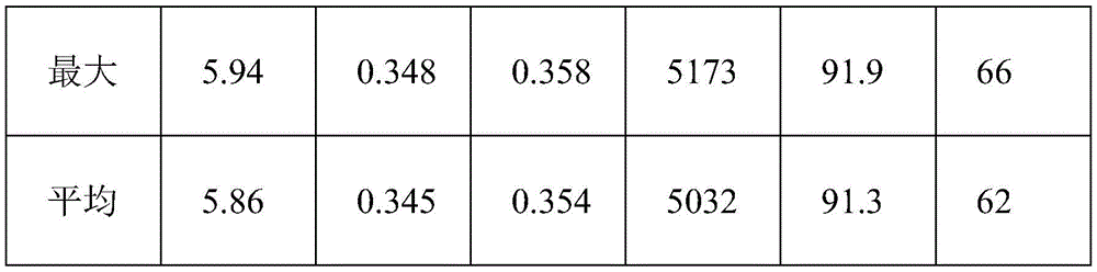
Tables 3, 4 and 5 show the light emitting device packages having the phosphor compositions according to the comparative examples, the second embodiment and the third embodiment when the color temperature of light emitted from the light emitting device packages is 5000K (absolute temperature scale), and show the characteristics of the emitted light.
[ TABLE 3 ]
| |
lm
|
Cx
|
Cy
|
CCT
|
CRI
|
R9
|
| Minimum size
|
6.63
|
0.340
|
0.350
|
4852
|
81.9
|
-1
|
| Maximum of
|
6.86
|
0.350
|
0.358
|
5180
|
83.3
|
6
|
| Average
|
6.77
|
0.345
|
0.354
|
5023
|
82.7
|
3 |
[ TABLE 4]
[ TABLE 5]
| |
lm
|
Cx
|
Cy
|
CCT
|
CRI
|
R9
|
| Minimum size
|
6.31
|
0.341
|
0.350
|
4873
|
89.3
|
22
|
| Maximum of
|
6.47
|
0.349
|
0.359
|
5160
|
91.0
|
30
|
| Average
|
6.38
|
0.345
|
0.354
|
5034
|
90.1
|
26 |
Fig. 6a to 6c show optical characteristics of the second and third embodiments of the phosphor composition together with a comparative example. In fig. 6a, the horizontal axis represents Cx value and the vertical axis represents Cy value. In fig. 6b, the horizontal axis represents the value of Cy, and the vertical axis represents the illuminance (lm). In fig. 6c, the horizontal axis represents wavelength and the vertical axis represents intensity (W).
In the comparative example, the green phosphor may be included at 85 wt% to 95 wt%, and the red phosphor may be included at 5 wt% to 15 wt%. The phosphor may be contained in the molding part of the light emitting device package at a weight ratio of 10 wt% to 30 wt%.
The Color Rendering Index (CRI) and the color rendering index (R9) of the light emitting device packages having the phosphor compositions according to the second and third embodiments shown in tables 4 and 5 were improved as compared to the CRT and R9 of the light emitting device packages having the phosphor compositions according to the comparative examples shown in table 3.
In a fourth embodiment of the phosphor composition, the weight ratio of the first phosphor is 1 wt% to 10 wt%, the weight ratio of the second phosphor is 75 wt% to 90 wt%, and the weight ratio of the third phosphor is 2 wt% to 15 wt%. The phosphor may be contained in the molding part of the light emitting device package at a weight ratio of 10 wt% to 30 wt%. In detail, the weight ratio of the first phosphor may be 5 to 9 wt%, the weight ratio of the second phosphor may be 82 to 90 wt%, and the weight ratio of the third phosphor may be 6 to 12 wt%. The phosphor may be contained in the molding part of the package at a weight ratio of 15 wt% to 25 wt%.
Table 6 and table 7 show the characteristics of light emitted from the light emitting device packages including the phosphor compositions according to the comparative examples and the fourth embodiment when the color temperature of light emitted from the light emitting device packages was 4000K (absolute temperature scale), respectively.
[ TABLE 6]
| |
lm
|
Cx
|
Cy
|
CCT
|
CRI
|
R9
|
| Minimum size
|
6.42
|
0.376
|
0.375
|
3951
|
83.2
|
10
|
| Maximum of
|
6.52
|
0.384
|
0.382
|
4099
|
84.0
|
15
|
| Average
|
6.47
|
0.380
|
0.378
|
4022
|
83.6
|
12 |
[ TABLE 7]
| |
lm
|
Cx
|
Cy
|
CCT
|
CRI
|
R9
|
| Minimum size
|
5.47
|
0.377
|
0.374
|
3924
|
91.6
|
60
|
| Maximum of
|
5.57
|
0.385
|
0.382
|
4090
|
93.1
|
67
|
| Average
|
5.52
|
0.381
|
0.378
|
4007
|
92.3
|
63 |
Fig. 7a to 7c show the optical characteristics of the fourth embodiment of the phosphor composition at this time together with the comparative example. In fig. 7a, the horizontal axis represents Cx value and the vertical axis represents Cy value. In fig. 7b, the horizontal axis represents the value of Cy, and the vertical axis represents the illuminance (lm). In fig. 7c, the horizontal axis represents wavelength and the vertical axis represents intensity (W).
In the comparative example, the green phosphor may be included at 85 wt% to 95 wt%, and the red phosphor may be included at 5 wt% to 15 wt%. The phosphor may be contained in the molding part of the light emitting device package at a weight ratio of 10 wt% to 30 wt%.
The Color Rendering Index (CRI) and the color rendering index (R9) of the light emitting device package having the phosphor composition according to the fourth embodiment shown in table 7 were improved as compared with the CRI and R9 of the light emitting device package having the phosphor composition according to the comparative example shown in table 6.
In a fifth embodiment of the phosphor composition, the weight ratio of the first phosphor is 1 wt% to 10 wt%, the weight ratio of the second phosphor is 75 wt% to 90 wt%, and the weight ratio of the third phosphor is 2 wt% to 20 wt%. The phosphor may be contained in the molding part of the light emitting device package at a weight ratio of 20 wt% to 40 wt%. In detail, the weight ratio of the first phosphor may be 2 to 7 wt%, the weight ratio of the second phosphor may be 77 to 85 wt%, and the weight ratio of the third phosphor may be 12 to 18 wt%. The phosphor may be contained in the molding part of the package at a weight ratio of 25 wt% to 35 wt%.
Table 8 and table 9 show the characteristics of light emitted from the light emitting device packages including the phosphor composition according to the comparative example and the fifth embodiment when the color temperature of light emitted from the light emitting device packages was 3000K (absolute temperature scale), respectively.
[ TABLE 8]
| |
lm
|
Cx
|
Cy
|
CCT
|
CRI
|
R9
|
| Minimum size
|
5.90
|
0.436
|
0.402
|
2933
|
81.6
|
3
|
| Maximum of
|
6.05
|
0.442
|
0.409
|
3040
|
82.6
|
8
|
| Average
|
6.00
|
0.439
|
0.406
|
2989
|
82.1
|
5 |
[ TABLE 9 ]
Fig. 8a to 8c show the optical characteristics of the fifth embodiment of the phosphor composition at this time together with the comparative example. In fig. 8a, the horizontal axis represents Cx value and the vertical axis represents Cy value. In fig. 8b, the ordinate represents illuminance (lm), the abscissa represents the value of Cy, and in fig. 8c, the abscissa represents wavelength and the ordinate represents intensity (W).
In the comparative example, the green phosphor may be included at 85 wt% to 95 wt%, and the red phosphor may be included at 5 wt% to 15 wt%. The phosphor may be contained in the molding part of the light emitting device package at a weight ratio of 10 wt% to 30 wt%.
The Color Rendering Index (CRI) and the color rendering index (R9) of the light emitting device package having the phosphor composition according to the fifth embodiment shown in table 9 were improved as compared with the CRI and R9 of the light emitting device package having the phosphor composition according to the comparative example shown in table 8.
In a sixth embodiment of the phosphor composition, the weight ratio of the first phosphor is 1 wt% to 10 wt%, the weight ratio of the second phosphor is 75 wt% to 90 wt%, and the weight ratio of the third phosphor is 2 wt% to 20 wt%. The phosphor may be included in the molding part of the light emitting device package at a weight ratio of 205 wt% to 45 wt%. In detail, the weight ratio of the first phosphor may be 3 to 9 wt%, the weight ratio of the second phosphor may be 74 to 82 wt%, and the weight ratio of the third phosphor may be 12 to 18 wt%. The phosphor may be contained in the molding part of the package at a weight ratio of 30 wt% to 40 wt%.
Table 10 and table 11 show the characteristics of light emitted from the light emitting device packages including the phosphor compositions according to the comparative example and the sixth embodiment when the color temperature of light emitted from the light emitting device packages was 2700K (absolute temperature scale), respectively.
[ TABLE 10 ]
[ TABLE 11 ]
| |
lm
|
Cx
|
Cy
|
CCT
|
CRI
|
R9
|
| Minimum size
|
4.65
|
0.455
|
0.406
|
2657
|
91
|
49
|
| Maximum of
|
4.99
|
0.461
|
0.412
|
2773
|
94
|
57
|
| Average
|
4.83
|
0.458
|
0.409
|
2719
|
92
|
53 |
Fig. 9a to 9c show the optical characteristics of the sixth embodiment of the phosphor composition at this time together with the comparative example. In fig. 9a, the horizontal axis represents Cx value and the vertical axis represents Cy value. In fig. 9b, the horizontal axis represents the value of Cy, and the vertical axis represents the illuminance (lm). In fig. 9c, the horizontal axis represents wavelength and the vertical axis represents intensity (W).
In the comparative example, the green phosphor may be included at 85 wt% to 95 wt%, and the red phosphor may be included at 5 wt% to 15 wt%. The phosphor may be contained in the molding part of the light emitting device package at a weight ratio of 10 wt% to 30 wt%.
The Color Rendering Index (CRI) and the color rendering index (R9) of the light emitting device package having the phosphor composition according to the sixth embodiment shown in table 11 were improved as compared with the CRI and R9 of the light emitting device package having the phosphor composition according to the comparative example shown in table 10.
Fig. 10 is a view showing changes in wavelength and intensity of red light according to the weight ratio of the first phosphor in the phosphor composition. As the weight ratio of the cyan phosphor as the first phosphor increases, the spectral intensity in the vicinity of 495nm gradually increases. Specifically, the fluorescence intensity increases by 2.5% to 3% every time the weight ratio of the first phosphor increases by 1 wt%, the spectral intensity at 555nm gradually decreases, and specifically, the intensity decreases by 1.5% to 2% when the weight ratio of the first phosphor increases by 1 wt%, and the intensity of the spectrum in the red wavelength region gradually increases by 0.2% when the weight ratio of the first phosphor increases by 1 wt%.
Fig. 11 is a view showing that the first phosphor is contained and the color rendering index and luminous flux of the phosphor composition are improved.
Light emitted from the phosphor composition according to the embodiment including a cyan phosphor (as a first phosphor) emitting light in a cyan wavelength region is emitted from the phosphor composition according to the comparative example shown by the solid line. The color rendering index is improved in the region a, the wavelength of light in the red wavelength region is shortened in the region B, and the luminous flux is increased, as compared with the emitted light.
Hereinafter, an image display apparatus and an illumination apparatus will be described as examples of an illumination system in which the light emitting device package 200 having the above-described phosphor composition is disposed.
A plurality of light emitting device packages 200 according to the embodiment may be arranged on a substrate, and a light guide plate, a prism sheet, a diffusion sheet, etc. may be disposed on an optical path of the light emitting device packages 200. The light emitting device package 200, the substrate, and the optical member may be used as a backlight unit.
In addition, a display apparatus, an indication apparatus, and a lighting apparatus including the light emitting device package 200 according to the embodiment may be implemented.
The display device includes a bottom cover, a reflector disposed on the bottom cover, a light emitting module for emitting light, a light guide plate disposed in front of the reflector for guiding the light emitted from the light emitting module to the front, an image signal output circuit connected to the display panel and supplying an image signal to the display panel, and a color filter disposed in front of the display panel. Here, the bottom cover, the reflector, the light emitting module, the light guide plate, and the optical sheet may form a backlight unit.
In addition, the lighting apparatus includes a substrate, a light source module including the light emitting device package 200 according to the present embodiment, a heat sink for dissipating heat of the light source module and an electrical signal provided from the outside, and a power supply unit. For example, the lighting device may include an electric lamp, a headlamp, or a street lamp.
A headlamp for a vehicle includes: a light emitting module including a light emitting device package 200 disposed on a substrate; a reflector that reflects light emitted from the light emitting module in a predetermined direction (e.g., forward); and a lamp cover reflecting the light reflected by the reflector and blocking or reflecting a portion of the light directed toward the lens, thereby providing a designer with a desired light distribution pattern.
In the case of the above-described video display apparatus and lighting apparatus, by using the phosphor composition or the light emitting device package of the above-described embodiment, the luminous flux and the color reproduction rate can be improved. In addition, under high temperature conditions, it is possible to reduce degradation of optical characteristics of the light emitting device and improve reliability.
While the invention has been described with reference to exemplary embodiments, it is to be understood that the invention is not limited to the disclosed exemplary embodiments, but, on the contrary, is intended to cover various modifications and equivalent arrangements included within the spirit and scope of the appended claims. It will be understood that various modifications and applications are possible. For example, each component specifically illustrated in the embodiments may be modified and implemented. It should be understood that the present invention may be embodied in many other specific forms without departing from its spirit or essential characteristics.