CN108291902B - Differential output of analog memory storing nanopore measurement samples - Google Patents
Differential output of analog memory storing nanopore measurement samples Download PDFInfo
- Publication number
- CN108291902B CN108291902B CN201680068430.4A CN201680068430A CN108291902B CN 108291902 B CN108291902 B CN 108291902B CN 201680068430 A CN201680068430 A CN 201680068430A CN 108291902 B CN108291902 B CN 108291902B
- Authority
- CN
- China
- Prior art keywords
- nanopore
- voltage
- state
- data
- measurement
- Prior art date
- Legal status (The legal status is an assumption and is not a legal conclusion. Google has not performed a legal analysis and makes no representation as to the accuracy of the status listed.)
- Active
Links
Images


Classifications
-
- G—PHYSICS
- G01—MEASURING; TESTING
- G01N—INVESTIGATING OR ANALYSING MATERIALS BY DETERMINING THEIR CHEMICAL OR PHYSICAL PROPERTIES
- G01N27/00—Investigating or analysing materials by the use of electric, electrochemical, or magnetic means
- G01N27/26—Investigating or analysing materials by the use of electric, electrochemical, or magnetic means by investigating electrochemical variables; by using electrolysis or electrophoresis
-
- B—PERFORMING OPERATIONS; TRANSPORTING
- B82—NANOTECHNOLOGY
- B82Y—SPECIFIC USES OR APPLICATIONS OF NANOSTRUCTURES; MEASUREMENT OR ANALYSIS OF NANOSTRUCTURES; MANUFACTURE OR TREATMENT OF NANOSTRUCTURES
- B82Y35/00—Methods or apparatus for measurement or analysis of nanostructures
-
- G—PHYSICS
- G01—MEASURING; TESTING
- G01N—INVESTIGATING OR ANALYSING MATERIALS BY DETERMINING THEIR CHEMICAL OR PHYSICAL PROPERTIES
- G01N33/00—Investigating or analysing materials by specific methods not covered by groups G01N1/00 - G01N31/00
- G01N33/48—Biological material, e.g. blood, urine; Haemocytometers
- G01N33/483—Physical analysis of biological material
- G01N33/487—Physical analysis of biological material of liquid biological material
- G01N33/48707—Physical analysis of biological material of liquid biological material by electrical means
- G01N33/48721—Investigating individual macromolecules, e.g. by translocation through nanopores
Landscapes
- Engineering & Computer Science (AREA)
- Health & Medical Sciences (AREA)
- Chemical & Material Sciences (AREA)
- Life Sciences & Earth Sciences (AREA)
- Physics & Mathematics (AREA)
- Biomedical Technology (AREA)
- Analytical Chemistry (AREA)
- Nanotechnology (AREA)
- Immunology (AREA)
- Biochemistry (AREA)
- Molecular Biology (AREA)
- Pathology (AREA)
- General Physics & Mathematics (AREA)
- General Health & Medical Sciences (AREA)
- Medicinal Chemistry (AREA)
- Biophysics (AREA)
- Hematology (AREA)
- Food Science & Technology (AREA)
- Spectroscopy & Molecular Physics (AREA)
- Urology & Nephrology (AREA)
- Crystallography & Structural Chemistry (AREA)
- Chemical Kinetics & Catalysis (AREA)
- Electrochemistry (AREA)
- Investigating Or Analyzing Materials By The Use Of Electric Means (AREA)
- Apparatus Associated With Microorganisms And Enzymes (AREA)
- Measuring Or Testing Involving Enzymes Or Micro-Organisms (AREA)
Abstract
公开了纳米孔测量电路。纳米孔测量电路包括纳米孔电极、第一模拟存储器和第二模拟存储器。纳米孔测量电路还包括将纳米孔电极选择性地连接到第一模拟存储器和第二模拟存储器中的至少一个的开关网络。
A nanopore measurement circuit is disclosed. The nanopore measurement circuit includes a nanopore electrode, a first analog memory, and a second analog memory. The nanopore measurement circuit also includes a switching network that selectively connects the nanopore electrode to at least one of the first and second analog memories.
Description
背景技术Background technique
近年来半导体产业内微小型化方面的进步使得生物技术专家能够开始将传统上庞大的感测工具打包到越来越小的形状因子中,打包到所谓的生物芯片上。常常,可以从生物芯片中导出的数据量由于在通信带宽方面的限制而受约束。随着生物芯片生成越来越多的信息,减小需要从生物芯片中导出的数据的量将是合期望的。Advances in microminiaturization within the semiconductor industry in recent years have enabled biotechnologists to begin packaging traditionally bulky sensing tools into increasingly smaller form factors, onto so-called biochips. Often, the amount of data that can be derived from a biochip is constrained by limitations in communication bandwidth. As biochips generate more and more information, it would be desirable to reduce the amount of data that needs to be derived from biochips.
附图说明Description of drawings
在以下详细描述和附图中公开了本发明的各种实施例。Various embodiments of the invention are disclosed in the following detailed description and accompanying drawings.
图1图示了基于纳米孔的定序芯片中的单元100的实施例。Figure 1 illustrates an embodiment of a
图2图示了利用Nano-SBS技术来执行核苷酸定序的单元200的实施例。Figure 2 illustrates an embodiment of a
图3图示了即将利用预加载的标签来执行核苷酸定序的单元的实施例。Figure 3 illustrates an embodiment of a unit to perform nucleotide sequencing with preloaded tags.
图4图示了用于利用预加载的标签来进行核酸定序的过程400的实施例。FIG. 4 illustrates an embodiment of a
图5A图示了在法拉第传导期间的小信号电路模型的实施例。5A illustrates an embodiment of a small signal circuit model during Faraday conduction.
图5B图示了在法拉第传导情况下PNTMC的不同状态。Figure 5B illustrates the different states of the PNTMC under Faraday conduction.
图6图示了被配置用于非法拉第和电容性耦合的测量的基于纳米孔的定序芯片中的单元的实施例。6 illustrates an embodiment of a cell in a nanopore-based sequencing chip configured for measurement of non-Faraday and capacitive coupling.
图7图示了针对非法拉第传导的小信号电路模型的实施例。7 illustrates an embodiment of a small signal circuit model for Faraday conduction.
图8A和图8B图示了双层的电容性响应的实施例。8A and 8B illustrate an example of the capacitive response of a double layer.
图9A和9B图示了在非法拉第AC调制情况下的纳米孔电流。9A and 9B illustrate nanopore currents with Faradaic AC modulation.
图10图示了处于稳定状态的峰值正电流根据占空比和所施加的电压而变化。Figure 10 illustrates peak positive current at steady state as a function of duty cycle and applied voltage.
图11图示了与图10的数据匹配的仿真模型的实施例。FIG. 11 illustrates an embodiment of a simulation model matched to the data of FIG. 10 .
图12A和12B图示了当所施加的信号具有50%占空比时的仿真结果。12A and 12B illustrate simulation results when the applied signal has a 50% duty cycle.
图13A图示了当所施加的信号具有25%占空比时的测量电流。Figure 13A illustrates the measured current when the applied signal has a 25% duty cycle.
图13B图示了当所施加的信号具有25%占空比时的仿真电流。Figure 13B illustrates the simulated current when the applied signal has a 25% duty cycle.
图14A图示了当所施加的信号具有50%占空比时施加到纳米孔的电压对时间。Figure 14A illustrates the voltage applied to the nanopore versus time when the applied signal has a 50% duty cycle.
图14B图示了当所施加的信号具有25%占空比时施加到纳米孔的电压对时间。Figure 14B illustrates the voltage applied to the nanopore versus time when the applied signal has a 25% duty cycle.
图15图示了用于标识分子的过程的实施例。Figure 15 illustrates an embodiment of a process for identifying molecules.
图16图示了基于纳米孔的定序芯片的单元中的电路1600的实施例。16 illustrates an embodiment of a
图17图示了基于纳米孔的定序芯片的单元中的电路1700的实施例,其中跨纳米孔施加的电压可以被配置成在纳米孔处于特定可检测状态中的时间段内变化。17 illustrates an embodiment of a circuit 1700 in a cell of a nanopore-based sequencing chip in which the voltage applied across the nanopore can be configured to vary over the period of time the nanopore is in a particular detectable state.
图18A和18B图示了基于纳米孔的定序芯片的单元中的电路(1800和1801)的附加实施例,其中跨纳米孔施加的电压可以被配置成在纳米孔处于特定可检测状态中的时间段内变化。Figures 18A and 18B illustrate additional embodiments of circuits (1800 and 1801 ) in a cell of a nanopore-based sequencing chip, wherein the voltage applied across the nanopore can be configured to cause the nanopore to be in a particular detectable state change over time.
图19图示了用于分析纳米孔内部的分子的过程1900的实施例,其中纳米孔被插入隔膜中。19 illustrates an embodiment of a
图20图示了当过程1900被执行且重复三次时跨纳米孔施加的电压对时间的曲线图的实施例。20 illustrates an example of a graph of voltage applied across a nanopore versus time when
图21图示了当纳米孔处于不同状态时跨纳米孔施加的电压对时间的曲线图的实施例。21 illustrates an example of a graph of voltage applied across a nanopore versus time when the nanopore is in different states.
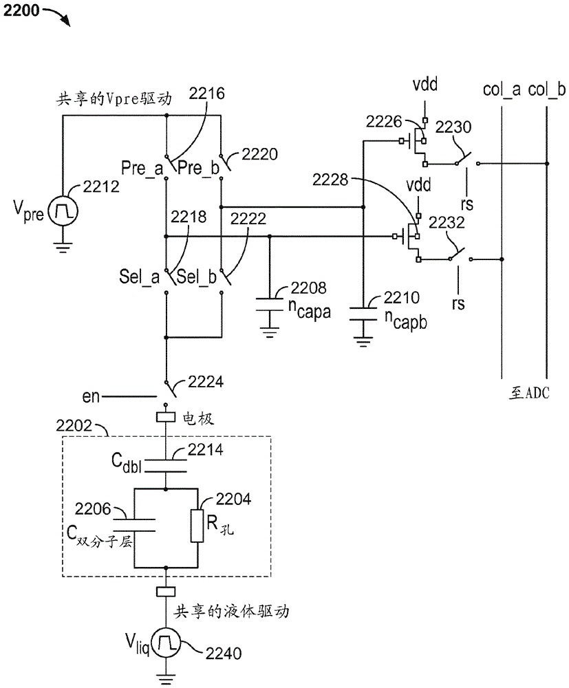
图22是图示基于纳米孔的定序芯片的单元的电路的实施例的电路图,其中该定序芯片包括用于存储测量值的模拟存储器。22 is a circuit diagram illustrating an embodiment of a circuit of a cell of a nanopore-based sequencing chip, wherein the sequencing chip includes an analog memory for storing measurements.
图23是图示了用于测量纳米孔的过程的实施例的流程图。23 is a flowchart illustrating an embodiment of a process for measuring nanopores.
图24是图示了当AC电压源被用作纳米孔的对电极的参考电压时的电路测量结果的图形的图。24 is a graph illustrating a graph of circuit measurements when an AC voltage source is used as a reference voltage for the counter electrode of the nanopore.
图25是图示了用于检测纳米孔的状态并自适应地处理纳米孔状态数据以优化要被输出的数据的系统的实施例的框图。25 is a block diagram illustrating an embodiment of a system for detecting the state of a nanopore and adaptively processing nanopore state data to optimize the data to be output.
图26是图示了用于报告纳米孔状态数据的过程的实施例的流程图。26 is a flowchart illustrating an embodiment of a process for reporting nanopore status data.
图27是图示了在参考AC电压源信号的循环期间接收的周期性电气测量样本的示例的图。27 is a diagram illustrating an example of periodic electrical measurement samples received during cycling of a reference AC voltage source signal.
图28是图示了用于自适应地分析要被输出的数据的过程的实施例的流程图。28 is a flowchart illustrating an embodiment of a process for adaptively analyzing data to be output.
图29是图示了用于确定压缩技术的过程的实施例的流程图。29 is a flowchart illustrating an embodiment of a process for determining a compression technique.
图30是图示了用于修改/过滤要被输出的数据的过程的实施例的流程图。30 is a flowchart illustrating an embodiment of a process for modifying/filtering data to be output.
图31是图示了用于处置穿过纳米孔多状态检测的过程的实施例的流程图。31 is a flowchart illustrating an embodiment of a process for handling multi-state detection through a nanopore.
具体实施方式Detailed ways
本发明可以以众多方式来实现,这些方式包括作为过程;装置;系统;物质组成;体现在计算机可读存储介质上的计算机程序产品;和/或处理器,诸如被配置成执行指令的处理器,所述指令被存储在耦合到该处理器的存储器上和/或由耦合到该处理器的存储器提供。在该说明书中,这些实现或本发明可以采取的任何其它形式可以被称为技术。一般地,可以在本发明的范围内变更所公开的过程的步骤的顺序。除非另外记载,否则可以将被描述为被配置成执行任务的诸如处理器或存储器之类的部件实现为被暂时配置成在给定时间执行该任务的一般部件或被制造成执行该任务的特定部件。如在本文中使用的,术语“处理器”指代被配置成处理诸如计算机程序指令之类的数据的一个或多个设备、电路和/或处理核。The invention can be implemented in numerous ways, including as a process; an apparatus; a system; a composition of matter; a computer program product embodied on a computer-readable storage medium; and/or a processor, such as a processor configured to execute instructions , the instructions are stored on and/or provided by a memory coupled to the processor. In this specification, these implementations, or any other form the invention may take, may be referred to as techniques. In general, the order of the steps of the disclosed processes may be varied within the scope of the invention. Unless otherwise noted, a component, such as a processor or memory, described as being configured to perform a task may be implemented as a general component temporarily configured to perform the task at a given time or as a specific component manufactured to perform the task part. As used herein, the term "processor" refers to one or more devices, circuits, and/or processing cores configured to process data, such as computer program instructions.
下面连同图示本发明的原理的附图提供本发明的一个或多个实施例的详细描述。本发明结合此类实施例被描述,但本发明不限于任何实施例。本发明的范围仅由权利要求限制并且本发明包含众多替代方案、修改和等同方案。以下描述中阐述了众多特定细节以便提供对本发明的透彻理解。出于举例的目的而提供了这些细节,并且可以在没有这些特定细节中的一些或全部的情况下根据权利要求实践本发明。出于清楚的目的,没有详细地描述在与本发明相关的技术领域中已知的技术材料以使得本发明不会被不必要地模糊。A detailed description of one or more embodiments of the invention is provided below in conjunction with the accompanying drawings that illustrate the principles of the invention. The invention is described in conjunction with such embodiments, but the invention is not limited to any embodiment. The scope of the invention is limited only by the claims and the invention encompasses numerous alternatives, modifications and equivalents. Numerous specific details are set forth in the following description in order to provide a thorough understanding of the present invention. These details are provided for the purpose of example and the invention may be practiced according to the claims without some or all of these specific details. For the purpose of clarity, technical material that is known in the technical fields related to the invention has not been described in detail so that the invention is not unnecessarily obscured.
具有大约一纳米内径的孔大小的纳米孔隔膜设备在快速核苷酸定序方面显示了希望。当跨沉浸于传导流体中的纳米孔施加电压电位时,可以观察到归因于跨纳米孔的离子传导的小离子电流。该电流的大小对孔大小敏感。Nanoporous membrane devices with pore sizes of about one nanometer inner diameter show promise in rapid nucleotide sequencing. When a voltage potential is applied across the nanopore immersed in a conducting fluid, a small ionic current due to ionic conduction across the nanopore can be observed. The magnitude of this current is sensitive to pore size.
基于纳米孔的定序芯片可以用于DNA定序。基于纳米孔的定序芯片包括被配置为阵列的大量传感器单元。例如,具有一百万个单元的阵列可以包括1000行×1000列个单元。Nanopore-based sequencing chips can be used for DNA sequencing. Nanopore-based sequencing chips include a large number of sensor cells configured as an array. For example, an array with one million cells may include 1000 rows by 1000 columns of cells.
图1图示了基于纳米孔的定序芯片中的单元100的实施例。隔膜102形成于单元的表面之上。在一些实施例中,隔膜102是脂质双分子层。包含可溶性蛋白质纳米孔跨膜分子复合物(PNTMC)和感兴趣的分析物的主体电解液(bulk electrolyte)114被直接放置到单元的表面上。单个PNTMC 104通过电穿孔而被插入到隔膜102中。阵列中的个体隔膜既不化学地也不电气地彼此连接。因此,阵列中的每个单元是独立的定序机器,产生对与PNTMC相关联的单个聚合物分子而言唯一的数据。PNTMC 104对分析物起作用并且通过另外的不可渗透的双分子层来调制离子电流。Figure 1 illustrates an embodiment of a
继续参考图1,模拟测量电路112连接到被电解液薄膜108所覆盖的金属电极110。电解液薄膜108通过离子不可渗透隔膜102与主体电解液114隔离。PNTMC 104穿过隔膜102并且提供用于离子电流从主体液体(bulk liquid)流到工作电极110的唯一路径。单元还包括对电极(CE)116,对电极116是电化学电位传感器。With continued reference to FIG. 1 , the
在一些实施例中,纳米孔阵列使用基于单分子纳米孔的合成定序(Nano-SBS)技术实现了并行定序。图2图示了利用Nano-SBS技术来执行核苷酸定序的单元200的实施例。在Nano-SBS技术中,将要被定序的模板202和先导物引入到单元200。针对该模板-先导物复合物,四个不同地加标签的核苷酸208被添加到主体水相。随着被正确加标签的核苷酸与聚合酶204复合,标签的尾部被定位在纳米孔206的桶状体中。保持在纳米孔206的桶状体中的标签生成唯一离子阻挡信号210,从而由于标签的不同化学结构而以电子方式标识所添加的碱基。In some embodiments, the nanopore array achieves parallel sequencing using single-molecule nanopore-based sequencing by synthesis (Nano-SBS) technology. Figure 2 illustrates an embodiment of a
图3图示了即将利用预加载的标签来执行核苷酸定序的单元的实施例。在隔膜302中形成纳米孔301。酶303(例如,聚合酶,诸如DNA聚合酶)与纳米孔相关联。在一些情况中,聚合酶303共价键合地附连到纳米孔301。聚合酶303与要被定序的核酸分子304相关联。在一些实施例中,核酸分子304是圆形的。在一些情况中,核酸分子304是线性的。在一些实施例中,核酸先导物305与核酸分子304的一部分杂交。聚合酶303使用单链核酸分子304作为模板来催化核苷酸306结合到先导物305上。核苷酸306包括标签种类(“标签”)307。Figure 3 illustrates an embodiment of a unit to perform nucleotide sequencing with preloaded tags.
图4图示了用于利用预加载的标签进行核酸定序的过程400的实施例。阶段A图示了如图3中描述的部件。阶段C示出了被加载到纳米孔中的标签。“被加载的”标签可以是被定位在纳米孔中和/或保持在纳米孔中或附近达可观测时间量的标签,所述可观测时间量例如0.1毫秒(ms)到10000 ms。在一些情况中,预加载的标签在从核苷酸释放之前被加载到纳米孔中。在一些实例中,如果在核苷酸结合事件时标签在被释放之后穿过纳米孔(和/或被纳米孔检测到)的概率合适地高,例如90%到99%,则标签被预加载。FIG. 4 illustrates an embodiment of a
在阶段A处,加标签的核苷酸(四个不同类型:A、T、G或C之一)不与聚合酶相关联。在阶段B处,加标签的核苷酸与聚合酶相关联。在阶段C处,聚合酶对接到纳米孔。标签在对接期间被电动力拉到纳米孔中,所述电动力诸如是在由跨隔膜和/或纳米孔施加的电压所生成的电场存在的情况下生成的力。At stage A, the tagged nucleotides (one of four different types: A, T, G or C) are not associated with the polymerase. At stage B, the tagged nucleotides are associated with the polymerase. At stage C, the polymerase is docked to the nanopore. The tag is pulled into the nanopore during docking by an electromotive force, such as a force generated in the presence of an electric field generated by a voltage applied across the membrane and/or nanopore.
相关联的加标签的核苷酸中的一些不是与核酸分子配对的碱基。这些非配对的核苷酸通常在一时间尺度内被聚合酶拒绝,该时间尺度比正确配对的核苷酸保持与聚合酶相关联的时间尺度短。由于非配对的核苷酸仅与聚合酶短暂地相关联,如图4中示出的过程400通常不前进超过阶段D。例如,非配对的核苷酸在阶段B处或在过程进入阶段C之后不久被聚合酶拒绝。Some of the associated tagged nucleotides are not bases paired with nucleic acid molecules. These unpaired nucleotides are typically rejected by the polymerase on a timescale that is shorter than the timescale over which correctly paired nucleotides remain associated with the polymerase. Since unpaired nucleotides are only briefly associated with the polymerase,
在聚合酶对接到纳米孔之前,纳米孔的电导是大约300皮西门子(300 pS)。在阶段C处,纳米孔的电导为大约60 pS、80 pS、100 pS或120 pS,它们对应于加标签的核苷酸的四个类型之一。聚合酶经受异构化和转磷酸反应以将核苷酸结合到生长的核酸分子中并且释放标签分子。特别地,当标签保持在纳米孔中时,由于标签的不同化学结构而生成唯一电导信号(例如,参见图2中的信号210),从而以电子方式标识所添加的碱基。重复所述循环(即,阶段A到E或者阶段A到F)允许对核酸分子定序。在阶段D处,所释放的标签穿过纳米孔。The conductance of the nanopore is approximately 300 picosiemens (300 pS) before the polymerase is docked to the nanopore. At stage C, the conductance of the nanopore is approximately 60 pS, 80 pS, 100 pS or 120 pS, which corresponds to one of the four types of tagged nucleotides. The polymerase undergoes isomerization and transphosphorylation reactions to incorporate nucleotides into growing nucleic acid molecules and release tag molecules. In particular, when the tag is retained in the nanopore, a unique conductance signal (eg, see
在一些情况中,未结合到生长的核酸分子中的加标签的核苷酸也将穿过纳米孔,如图4的阶段F中所看到的。在一些实例中,未被结合的核苷酸可以被纳米孔检测到,但该方法提供了用于至少部分地基于在纳米孔中检测到核苷酸的时间来区分被结合的核苷酸与未被结合的核苷酸的手段。键合到未被结合的核苷酸的标签快速地穿过纳米孔并且在短时间段(例如,小于10ms)内被检测到,而被键合到被结合的核苷酸的标签加载到纳米孔中并且在长时间段(例如,至少10 ms)内被检测到。In some cases, tagged nucleotides not incorporated into the growing nucleic acid molecule will also pass through the nanopore, as seen in stage F of FIG. 4 . In some instances, unbound nucleotides can be detected by the nanopore, but the method provides for distinguishing bound nucleotides from means of unbound nucleotides. Tags bound to unbound nucleotides quickly pass through the nanopore and are detected within a short period of time (eg, less than 10 ms), while tags bound to bound nucleotides are loaded into the nanopore. holes and are detected over a long period of time (eg, at least 10 ms).
两个类型的离子流可以通过 PNTMC-法拉第传导和非法拉第传导来驱动。在法拉第传导中,化学反应发生在金属电极的表面处。法拉第电流是通过电极处的一些化学物质的还原或氧化而生成的电流。在非法拉第传导中,没有化学反应发生在金属的表面处。金属电极与电解液的薄膜之间的双层电容上改变的电位驱动离子流。Two types of ion currents can be driven by PNTMC-Faraday conduction and Faraday conduction. In Faraday conduction, chemical reactions take place at the surface of the metal electrode. Faradaic current is the current generated by the reduction or oxidation of some chemical species at the electrodes. In Faraday conduction, no chemical reaction takes place at the surface of the metal. The changing potential on the double layer capacitance between the metal electrode and the thin film of electrolyte drives the ion flow.
由法拉第传导导致的离子流具有许多缺点。因为电极中的金属随着离子电流流过PNTMC而被消耗并且耗尽,所以电极的操作寿命是受限的,如下面将更详细地描述的。Ionic currents due to Faraday conduction have a number of disadvantages. Because the metal in the electrodes is consumed and depleted as the ionic current flows through the PNTMC, the operational lifetime of the electrodes is limited, as will be described in more detail below.
图5A图示了在法拉第传导期间的小信号电路模型的实施例。PNTMC和WE被表示为小信号电路模型中的简单电阻器。图5B图示了在法拉第传导情况下PNTMC的不同状态。离子电流流动i(t)具有五个状态:在开放的纳米孔通道(未示出)的情况下的最高电流状态,以及与键合到PNTMC的活性位点的核苷酸的四个不同类型中的每个类型对应的四个较低电流状态。正电流流动i(t)描述了电子进入VCE,RE节点并且离开VWE节点。阴离子(例如,Cl-)离开CE,流过主体电解液,经由PNTMC穿过脂质双分子层,并且继续通过电解液的薄膜并且与WE的金属组合。5A illustrates an embodiment of a small signal circuit model during Faraday conduction. PNTMC and WE are represented as simple resistors in the small-signal circuit model. Figure 5B illustrates the different states of the PNTMC under Faraday conduction. The ionic current flow i(t) has five states: the highest current state in the case of an open nanopore channel (not shown), and four different types with nucleotides bound to the active site of PNTMC There are four lower current states for each type in . Positive current flow i(t) describes electrons entering the V CE, RE node and leaving the V WE node. Anions (eg, Cl − ) exit the CE, flow through the bulk electrolyte, cross the lipid bilayer via the PNTMC, and continue through the membrane of the electrolyte and combine with the metals of the WE.
例如,针对具有银金属(Ag)的电极,化学反应是:For example, for an electrode with silver metal (Ag), the chemical reaction is:
方程1。
如上面在方程1中所示,针对穿过PNTMC的每个氯阴离子(Cl-),金属银的原子被转换成不溶性盐,氯化银(AgCl)。在一些情况中,银在数分钟的操作内被耗尽。As shown above in
为了避免金属电极的耗尽,可以通过施加负电压达类似的持续时间来逆转离子电流流动的方向,使得氯化银(AgCl)被转换回银金属。然而,以该方式的再充电或刷新使得银在金属电极的表面上被再沉积为毛发状的特征,这可能影响总体性能,尤其是具有较小单元几何形状并且因此具有较小电极的芯片中的总体性能。To avoid depletion of the metal electrode, the direction of ionic current flow can be reversed by applying a negative voltage for a similar duration, so that silver chloride (AgCl) is converted back to silver metal. However, recharging or refreshing in this manner causes silver to redeposit as hair-like features on the surface of the metal electrodes, which may affect overall performance, especially in chips with smaller cell geometries and thus smaller electrodes overall performance.
另一方式是通过如下方式来延迟金属电极的耗尽:施加电压以将聚合酶牵引到纳米孔并且将标签拉过纳米孔或拉到纳米孔附近以用于检测,并且然后关断电压达一时间段,这将使得标签被从纳米孔释放。由于在电压被关断时不存在电流,所以较少的银原子被转换并且金属电极的寿命被延长。然而,检测时间被相应地减少。Another way is to delay the depletion of the metal electrode by applying a voltage to pull the polymerase to the nanopore and the label through or near the nanopore for detection, and then turning off the voltage for a The time period that will allow the label to be released from the nanopore. Since there is no current flow when the voltage is turned off, fewer silver atoms are converted and the life of the metal electrode is extended. However, the detection time is reduced accordingly.
除了金属电极的耗尽之外,法拉第传导还导致单元内的主体电解液的浓度随时间过去而不平衡。例如,在一个电极处存在KCl分子的净增益,但在相对电极处存在KCl分子的净损耗。在一个电极处的这种盐浓度积累和在相对电极处的盐耗尽在所述单元内产生不合期望的渗透压。In addition to the depletion of the metal electrodes, Faradaic conduction causes the concentration of the bulk electrolyte within the cell to become unbalanced over time. For example, there is a net gain of KCl molecules at one electrode, but a net loss of KCl molecules at the opposite electrode. This accumulation of salt concentration at one electrode and depletion of salt at the opposite electrode creates undesirable osmotic pressure within the cell.
通过PNTMC的替代类型的离子流经由非法拉第传导。在非法拉第传导中,没有化学反应(化学物质的还原或氧化)发生在金属的表面处。跨金属电极与电解液的薄膜之间的双层电容的改变的电位驱动离子流。An alternative type of ion current through PNTMC is conducted via Faraday. In Faraday conduction, no chemical reaction (reduction or oxidation of chemicals) takes place at the surface of the metal. The changing potential across the double layer capacitance between the metal electrode and the thin film of electrolyte drives ion flow.
针对非法拉第传导,金属电极可以由耐腐蚀和氧化的金属制成。例如,诸如铂或金之类的贵金属难以氧化,并且甚至当它们氧化时,该过程也是容易逆转的。当将小电位(例如,相对于VCE小于+/- 1 V)施加于电解液中的铂/金时,除初始电容性瞬变现象之外,没有离子电流流动。这允许从金属遂穿到氧化还原(还原-氧化)活性种类中的电子的测量,该氧化还原活性种类被混合到电极中。在电解液中没有氧化还原活性种类(诸如铁氰化物或亚铁氰化物)的情况下,没有稳定状态的离子(或者电子或空穴)电流流过金属-液体界面。不管铂/金与电解液之间的化学(即,键合)反应的缺乏,响应于所施加的电位,因为液体-金属界面处的离子耗尽区的增长和收缩而存在电解液中离子的暂时物理位移。该离子耗尽区在电化学用语中被称为 “双层”。使用电气工程模型,形成平行板电容器,其中金属是一个板,耗尽区为电介质并且液体中离子的弥漫分布是另一个板。For Faraday conduction, the metal electrodes may be made of corrosion and oxidation resistant metals. For example, noble metals such as platinum or gold are difficult to oxidize, and even when they do, the process is easily reversed. When a small potential (eg, less than +/- 1 V relative to VCE ) is applied to platinum/gold in the electrolyte, no ionic current flows except for the initial capacitive transient. This allows the measurement of electrons tunneling from the metal into redox (reduction-oxidation) active species that are mixed into the electrode. In the absence of redox-active species such as ferricyanide or ferrocyanide in the electrolyte, there is no steady-state ionic (or electron or hole) current flowing through the metal-liquid interface. Regardless of the lack of chemical (ie, bonding) reactions between platinum/gold and the electrolyte, in response to the applied potential, there is a Temporary physical displacement. This ion depletion region is called a "bilayer" in electrochemical parlance. Using electrical engineering models, parallel plate capacitors are formed where the metal is one plate, the depletion region is the dielectric and the diffuse distribution of ions in the liquid is the other plate.
图6图示了被配置用于非法拉第和电容性耦合的测量的基于纳米孔的定序芯片中的单元的实施例。脂质双分子层602形成于单元的表面之上。包含可溶性蛋白质纳米孔跨膜分子复合物(PNTMC)和感兴趣的分析物的电解液614被直接放置到单元的表面上。单个PNTMC 604通过电穿孔而被插入到脂质双分子层602中。阵列中的个体脂质双分子层没有化学或电气地彼此连接。因此,阵列中的每个单元是独立的定序机器,其产生对与PNTMC相关联的单个聚合物分子而言唯一的数据。该单元包括用于进行非法拉第和电容性耦合的测量的模拟测量电路612。测量结果被转换成数字信息并且传输离开该单元。在一些实施例中,传输数据速率大约为每秒数吉比特。在一些实施例中,现场可编程门阵列(FPGA)或专用集成电路(ASIC)接收所传输的数据,处理该数据,并且将该数据转发到计算机。6 illustrates an embodiment of a cell in a nanopore-based sequencing chip configured for measurement of non-Faraday and capacitive coupling. A lipid bilayer 602 is formed on the surface of the cell. An electrolyte 614 containing a soluble protein nanopore transmembrane molecular complex (PNTMC) and an analyte of interest is placed directly on the surface of the cell. A single PNTMC 604 is inserted into the lipid bilayer 602 by electroporation. The individual lipid bilayers in the array are not chemically or electrically connected to each other. Thus, each unit in the array is an independent sequencing machine that generates data unique to a single polymer molecule associated with the PNTMC. The unit includes an analog measurement circuit 612 for making measurements of Faraday and capacitive coupling. The measurement results are converted into digital information and transmitted away from the unit. In some embodiments, the transfer data rate is on the order of gigabits per second. In some embodiments, a field programmable gate array (FPGA) or application specific integrated circuit (ASIC) receives the transmitted data, processes the data, and forwards the data to a computer.
继续参考图6,模拟测量电路612连接到被电解液的薄膜608所覆盖的金属电极610。电解液的薄膜608通过离子不可渗透脂质双分子层602与主体电解液614隔离。PNTMC604穿过脂质双分子层602并且提供用于从主体液体到金属电极610的离子流动的唯一路径。金属电极610也被称为工作电极(WE)。针对非法拉第传导,金属电极610可以由耐腐蚀和氧化的金属制成,例如铂、金和石墨。金属电极610可以是海绵状电极,如下面将更详细地描述的。单元还包括对电极/参考电极(CE/RE)616,其是电化学电位传感器。With continued reference to FIG. 6, an analog measurement circuit 612 is connected to a metal electrode 610 covered by a thin film 608 of electrolyte. The thin film 608 of electrolyte is isolated from the bulk electrolyte 614 by the ion-impermeable lipid bilayer 602 . PNTMC 604 passes through lipid bilayer 602 and provides the only path for ionic flow from the bulk liquid to metal electrode 610 . The metal electrode 610 is also referred to as the working electrode (WE). For Faraday conduction, the metal electrode 610 may be made of corrosion and oxidation resistant metals such as platinum, gold and graphite. Metal electrode 610 may be a sponge electrode, as will be described in more detail below. The cell also includes a counter/reference electrode (CE/RE) 616, which is an electrochemical potentiometric sensor.
图7图示了针对非法拉第传导的小信号电路模型的实施例。PNTMC被表示为小信号电路模型中的简单电阻器702。双层电容被表示为小信号电路模型中的电容器704。在一些实施例中,图7中的V1被设置成距地的增量电压,例如500 mV,而V2被设置成V1加上所施加的信号,例如所施加的从10Hz到1kHz的AC信号。7 illustrates an embodiment of a small signal circuit model for Faraday conduction. PNTMC is represented as a simple resistor 702 in the small signal circuit model. Double layer capacitance is represented as capacitor 704 in the small signal circuit model. In some embodiments, V1 in Figure 7 is set to an incremental voltage from ground, eg, 500 mV, and V2 is set to V1 plus an applied signal, eg, an applied voltage from 10 Hz to 1 kHz AC signal.
在一些实施例中,所施加的信号是AC信号。在一个极性处,所施加的AC信号将聚合酶牵引到纳米孔并且将标签牵引过纳米孔或牵引到纳米孔附近以用于检测。当所施加的AC信号的极性逆转时,标签被从纳米孔释放,并且电极被再充电/刷新以使得没有对金属电极进行电化学改变。随着AC信号重复地改变极性,标签的与加标签的核苷酸相关联的部分被引导到纳米孔中并且被引导离开纳米孔达多次。单个标签的该重复性加载和排出允许该标签被多次读取。多个读数可以实现对误差(诸如与标签穿入和/或穿出纳米孔相关联的误差)的纠正。In some embodiments, the applied signal is an AC signal. At one polarity, the applied AC signal pulls the polymerase to the nanopore and the label through or near the nanopore for detection. When the polarity of the applied AC signal is reversed, the tags are released from the nanopore and the electrodes are recharged/refreshed so that no electrochemical changes are made to the metal electrodes. As the AC signal repeatedly changes polarity, the portion of the tag associated with the tagged nucleotide is directed into the nanopore and out of the nanopore multiple times. This repetitive loading and ejection of a single label allows the label to be read multiple times. Multiple readings may enable correction of errors, such as those associated with tag penetration and/or penetration of the nanopore.
在一些实施例中,至少部分地基于加标签的核苷酸与聚合酶相关联的时间段来选取AC信号的频率。AC信号的频率应当允许与聚合酶相关联的加标签的核苷酸被至少一次牵引且加载到纳米孔中达充足的时间长度以使得该标签可以被检测到;否则,标签中的与聚合酶相关联的一些标签不能被系统检测到。换言之,采样应当处于比事件序列发生的速率更快的速率,使得没有事件被错过。In some embodiments, the frequency of the AC signal is chosen based, at least in part, on the time period during which the tagged nucleotides are associated with the polymerase. The frequency of the AC signal should allow the tagged nucleotides associated with the polymerase to be pulled and loaded into the nanopore at least once for a sufficient length of time to allow the tag to be detected; Some associated tags cannot be detected by the system. In other words, the sampling should be at a faster rate than the sequence of events occurs so that no events are missed.
继续参考图6,在脂质双分子层602形成之前,主体电解液614与工作电极610直接接触,因此在电解液与工作电极之间产生短路。图8A和图8B图示了双层的电容性响应的实施例。所述图图示了在电解液与工作电极之间短路的情况下双层的属性。在该示例中,电解液包含0.5 M乙酸钾和10mM KCl。对电极616包括AgCl。工作电极610是具有电镀铂的铂电极。水粘度防止容易响应于所施加的场的离子流动;这被显示为双层电容性响应中的串联电阻。该电阻限制如图8A中所示的峰值电流。可以在响应的衰减中看出RC电化学连接的串联性质,响应的衰减由RC时间常数表征。在图8B中,电流被示出下降到exp (-25) = 13.8pA,低于系统的检测极限。这展示了分流电阻(从电气视角)和法拉第电流(从电化学视角)二者的缺乏。With continued reference to Figure 6, prior to the formation of the lipid bilayer 602, the bulk electrolyte 614 is in direct contact with the working electrode 610, thus creating a short circuit between the electrolyte and the working electrode. 8A and 8B illustrate an example of the capacitive response of a double layer. The figure illustrates the properties of the bilayer in the case of a short circuit between the electrolyte and the working electrode. In this example, the electrolyte contains 0.5 M potassium acetate and 10 mM KCl. The counter electrode 616 includes AgCl. The working electrode 610 is a platinum electrode with electroplating platinum. Water viscosity prevents ion flow that readily responds to the applied field; this is shown as series resistance in the capacitive response of the double layer. This resistor limits the peak current as shown in Figure 8A. The tandem nature of the RC electrochemical connection can be seen in the decay of the response, which is characterized by the RC time constant. In Figure 8B, the current is shown to drop to exp (-25) = 13.8 pA, below the detection limit of the system. This demonstrates the lack of both shunt resistance (from an electrical perspective) and Faradaic current (from an electrochemical perspective).
工作电极610被配置成将针对给定体积的其表面积最大化。随着表面积增加,该双层的电容增加,并且可以在电容器被充电之前利用相同施加的电位使较大量的离子移位。参考图7,阻抗C双层= 
例如,可以通过使得电极成“海绵状”而增加工作电极的表面积。在一些实施例中,在存在清洁剂的情况下,可以通过将铂金属电镀到5微米直径的光滑铂电极上来增强双层到主体液体的电容。清洁剂在铂金属中产生纳米级空隙空间,使得它成“海绵状”。铂海绵吸收电解液并且产生大有效表面积(例如,电极自上而下面积的每平方微米33 pF)。使双层表面积最大化产生“DC阻挡”电容器,由此双层上的电压达到稳定状态并且在操作期间几乎不改变。串联PNTMC电阻(图7中的RPNTMC)和双层电容(图7中的C双层)形成低频零,其充当高通滤波器。在一个示例中,RPNTMC大约10千兆欧姆,C双层 大约800pF,导致大约10千兆欧姆 * 大约800pF = 大约8秒的时间常数。对在100 Hz处的测量进行斩波,然后拒绝DC漂移并且使测量到的标签中的低频信息内容衰减到以前的1/1000。For example, the surface area of the working electrode can be increased by making the electrode "sponge-like". In some embodiments, bilayer-to-bulk liquid capacitance can be enhanced by electroplating platinum metal onto a 5 micron diameter smooth platinum electrode in the presence of a cleaning agent. The detergent creates nanoscale void spaces in the platinum metal, making it "sponge-like". The platinum sponge absorbs the electrolyte and creates a large effective surface area (eg, 33 pF per square micrometer of electrode top-down area). Maximizing the surface area of the double layer creates a "DC blocking" capacitor, whereby the voltage across the double layer reaches a steady state and hardly changes during operation. The series PNTMC resistance (R PNTMC in Figure 7) and double layer capacitance (C double layer in Figure 7) form a low frequency zero, which acts as a high-pass filter. In one example, the R PNTMC is about 10 gigaohms and the C bilayer is about 800 pF, resulting in a time constant of about 10 gigaohms * about 800 pF = about 8 seconds. The measurement at 100 Hz is chopped, then DC drift is rejected and the low frequency information content in the measured tag is attenuated to 1/1000 of the previous.
在没有任何标签存在的情况下,PNTMC的表现与阿尔法溶血素蛋白质纳米孔类似。溶血素纳米孔具有根据方波驱动的占空比来改变其偏置的整流特性。不同于法拉第传导情况,施加到电极的绝对电压不与施加到纳米孔的电压相同:双层上的电压使施加到纳米孔的电位偏置,并且该偏置与占空比一起改变。In the absence of any tags, PNTMC behaves similarly to the alpha hemolysin protein nanopore. The hemolysin nanopore has a rectifying characteristic that changes its bias according to the duty cycle of the square wave drive. Unlike the Faraday conduction case, the absolute voltage applied to the electrodes is not the same as the voltage applied to the nanopore: the voltage across the bilayer biases the potential applied to the nanopore, and this bias changes along with the duty cycle.
图9A和9B图示了在非法拉第AC调制情况下的。在该示例中,所施加的信号是处于5Hz的具有50%占空比的200 mV峰到峰方波。电解液包含0.5 M乙酸钾和10mM KCl。对电极616包括AgCl。工作电极610是具有电镀铂的铂电极。9A and 9B illustrate in the case of Faraday AC modulation. In this example, the applied signal is a 200 mV peak-to-peak square wave at 5 Hz with a 50% duty cycle. The electrolyte contains 0.5 M potassium acetate and 10 mM KCl. The counter electrode 616 includes AgCl. The working electrode 610 is a platinum electrode with electroplating platinum.
图9A示出了当具有正极性的200 mV被施加到纳米孔时的启动瞬变现象,指示在直接施加200 mV的情况下的开放通道电流近似为70 pA。图9A示出了稳定状态在大约20秒之后达到。在图9B中,可以观察到双层电容器上的电压的衰减速率。衰减速率由双层电容和纳米孔负载电阻的大小确定。Figure 9A shows the start-up transient when 200 mV with positive polarity is applied to the nanopore, indicating that the open channel current is approximately 70 pA with a direct application of 200 mV. Figure 9A shows that the steady state is reached after approximately 20 seconds. In Figure 9B, the decay rate of the voltage across the double layer capacitor can be observed. The decay rate is determined by the size of the double layer capacitance and nanopore load resistance.
图10图示了处于稳定状态的峰值正电流根据占空比和所施加的电压而变化。曲线1010示出了当所施加的电压为200 mV峰到峰方波时相对不同的占空比绘制的以安培(A)为单位的稳定状态峰值电流。曲线1020示出了当所施加的电压为100 mV峰到峰方波时相对不同的占空比绘制的稳定状态峰值电流(以A为单位)。在该示例中,电解液包含0.5 M乙酸钾和10mM KCl。对电极616包括AgCl。工作电极610是具有电镀铂的铂电极。由于溶血素纳米孔具有整流特性(或是非欧姆的),与施加正极性电压时相比,要求更大量值的负极性电压来传递相同量值的电流。峰值正电流随着占空比增加而下降。占空比越低,通过双层电容施加到纳米孔的正电压就越高。Figure 10 illustrates peak positive current at steady state as a function of duty cycle and applied voltage.
图11图示了与图10的数据匹配的仿真模型的实施例。该仿真被构造以估计纳米孔上的实际电压,该实际电压由于与纳米孔串联连接的双层电容器而不与施加到工作电极的电压相同。在非法拉第情况中不能直接测量该电压。乙酸钾中的非线性被假定与1M氯化钾非线性成正比。图12A和12B图示了当所施加的信号具有50%占空比时的仿真结果。在图12B中,由于溶血素纳米孔的整流特性,衰减的斜坡对于正电流比负电流而言更陡峭,该溶血素纳米孔被利用图11中的多项式方程B1和B2建模。FIG. 11 illustrates an embodiment of a simulation model matched to the data of FIG. 10 . The simulation is constructed to estimate the actual voltage across the nanopore, which is not the same as the voltage applied to the working electrode due to the double layer capacitor connected in series with the nanopore. This voltage cannot be measured directly in the Faraday case. The nonlinearity in potassium acetate is assumed to be proportional to the nonlinearity in 1 M potassium chloride. 12A and 12B illustrate simulation results when the applied signal has a 50% duty cycle. In FIG. 12B , the ramp of decay is steeper for positive currents than for negative currents due to the rectifying properties of the hemolysin nanopore, which is modeled using polynomial equations B1 and B2 in FIG. 11 .
图13A图示了当所施加的信号具有25%占空比时的测量电流。图13B图示了当所施加的信号具有25%占空比时的仿真电流。这些图图示了在25%的较低占空比的情况下,通过纳米孔的正电流的量值(43pA)比通过纳米孔的负电流的量值(-13 pA)大得多。为了实现在稳定状态下没有分流电阻(没有法拉第电流),在一个震荡周期内通过所述双层的正和负电荷的总和应当为零。当i = dQ/dt,其中i=电流并且Q=电荷时,在电流对时间的图形中,电荷为曲线以下的面积。例如,如果在正极性的电流对时间曲线图的曲线以下的面积(图13B的面积1302)与在负极性的电流对时间曲线图的曲线以下的面积(图13B的面积1304)粗略相同,则在一个震荡周期内通过所述双层的正和负电荷的总和接近零。Figure 13A illustrates the measured current when the applied signal has a 25% duty cycle. Figure 13B illustrates the simulated current when the applied signal has a 25% duty cycle. The figures illustrate that at a lower duty cycle of 25%, the magnitude of positive current through the nanopore (43 pA) is much larger than the magnitude of negative current through the nanopore (-13 pA). To achieve no shunt resistance (no Faradaic current) in steady state, the sum of the positive and negative charges passing through the double layer during one oscillation cycle should be zero. When i = dQ/dt, where i=current and Q=charge, the charge is the area under the curve in a graph of current versus time. For example, if the area under the curve of the current versus time graph of positive polarity (area 1302 of FIG. 13B ) is roughly the same as the area under the curve of the current versus time graph of negative polarity (area 1304 of FIG. 13B ), then The sum of the positive and negative charges passing through the bilayer during one oscillation cycle approaches zero.
图14A图示了当所施加的信号具有50%占空比时施加到纳米孔的电压对时间。图14B图示了当所施加的信号具有25%占空比时施加到纳米孔的电压对时间。在图14B中的较低占空比的情况下,施加到纳米孔的电压较高,该电压以较高的效力朝着纳米孔牵引聚合酶和标签。在图14A中的较长占空比的情况下,当核苷酸特有标签就位时,较多时间花费在读取和检测标签上。Figure 14A illustrates the voltage applied to the nanopore versus time when the applied signal has a 50% duty cycle. Figure 14B illustrates the voltage applied to the nanopore versus time when the applied signal has a 25% duty cycle. With the lower duty cycle in Figure 14B, the voltage applied to the nanopore is higher, which pulls the polymerase and label toward the nanopore with higher efficacy. With the longer duty cycle in Figure 14A, when the nucleotide-specific tag is in place, more time is spent reading and detecting the tag.
图15图示了用于标识分子的过程的实施例。在1502处,通过在第一时段期间向电极对(例如,工作电极和对/参考电极)施加第一电压信号而将分子牵引到纳米孔,其中第一电压信号引起通过纳米孔的第一离子电流,第一离子电流指示接近纳米孔的分子的一部分(例如,加标签的核苷酸)的属性。例如,四个类型的加标签的核苷酸具有不同的属性并且当特定类型的加标签的核苷酸被牵引到纳米孔中时,指示所述属性的离子电流流过纳米孔。Figure 15 illustrates an embodiment of a process for identifying molecules. At 1502, molecules are drawn to the nanopore by applying a first voltage signal to the electrode pair (eg, the working electrode and the counter/reference electrode) during a first period of time, wherein the first voltage signal causes a first ion to pass through the nanopore The current, the first ionic current, is indicative of a property of a portion of a molecule (eg, a tagged nucleotide) proximate to the nanopore. For example, four types of tagged nucleotides have different properties and when a particular type of tagged nucleotide is pulled into a nanopore, an ionic current that is indicative of that property flows through the nanopore.
在1504处,通过在第二时段期间向电极对施加第二电压信号而从纳米孔释放分子,其中第二电压信号引起通过纳米孔的第二离子电流。At 1504, molecules are released from the nanopore by applying a second voltage signal to the electrode pair during a second period of time, wherein the second voltage signal causes a second ionic current through the nanopore.
在1506处,至少部分地基于包括第一离子电流和第二离子电流的通过纳米孔的净离子电流来确定第一时段和第二时段。例如,第一时段和第二时段可以被确定成使得净离子电流减小。在一些实施例中,通过将第二电压信号设置成关断来减小净离子电流。当第二电压信号被关断时,第二离子电流变成零并且金属电极的耗尽被延迟,如上面所解释的。在一些实施例中,通过将第二电压信号设置成具有与第一电压信号相对的极性的信号来减小净离子电流。例如,第一电压信号与第二电压信号之间的交替产生AC信号。第二离子电流抵消第一离子电流,因此减小通过纳米孔的净离子电流。如图10中所示,电流根据占空比和所施加的电压而变化。因此,占空比(即,第一时段和第二时段)可以被调整成使得在第一离子电流的曲线以下的面积与在第二离子电流的曲线以下的面积基本上相同,以使得在一个震荡周期(即,第一时段和第二时段)内通过所述双层的正和负电荷的总和接近于零。At 1506, the first period and the second period are determined based at least in part on the net ionic current through the nanopore including the first ionic current and the second ionic current. For example, the first period of time and the second period of time may be determined such that the net ionic current decreases. In some embodiments, the net ionic current is reduced by setting the second voltage signal off. When the second voltage signal is turned off, the second ionic current becomes zero and the depletion of the metal electrode is delayed, as explained above. In some embodiments, the net ionic current is reduced by setting the second voltage signal to a signal having an opposite polarity to the first voltage signal. For example, alternating between the first voltage signal and the second voltage signal produces an AC signal. The second ionic current counteracts the first ionic current, thus reducing the net ionic current through the nanopore. As shown in Figure 10, the current varies according to the duty cycle and the applied voltage. Therefore, the duty cycle (ie, the first period and the second period) can be adjusted such that the area under the curve of the first ion current is substantially the same as the area under the curve of the second ion current, such that in a The sum of the positive and negative charges through the bilayer during the period of oscillation (ie, the first and second periods) is close to zero.
图16图示了基于纳米孔的定序芯片的单元中的电路1600的实施例。如上面所提及的,当标签保持在纳米孔1602中时,由于标签的不同化学结构而生成唯一电导信号(例如,参见图2中的信号210),从而以电子方式标识所添加的碱基。图16中的电路在测量电流流动时维持跨纳米孔1602的恒定电压。特别地,该电路包括运算放大器1604和通过设备1606,运算放大器1604和通过设备1606维持跨纳米孔1602的恒定电压等于Va或Vb。流过纳米孔1602的电流在电容器ncap 1608处被积分,并且由模数(ADC)转换器1610测量。16 illustrates an embodiment of a
然而,电路1600具有许多缺点。缺点之一是电路1600仅测量单向电流流动。另一缺点是电路1600中的运算放大器1604可能引入许多性能问题。例如,运算放大器1604的偏移电压和温度漂移可能使得跨纳米孔1602施加的实际电压在不同单元之间不同。跨纳米孔1602施加的实际电压可能漂移高于或低于期望值数十毫伏,从而引起显著的测量不准确性。另外,运算放大器噪声可能引起附加的检测误差。另一缺点是电路的用于在进行电流流动测量时维持跨纳米孔的恒定电压的部分是面积加强的(area-intensive)。例如,运算放大器1604在单元中比其它部件占据显著更多的空间。随着基于纳米孔的定序芯片被缩放成包括越来越多的单元,由运算放大器占据的面积可能增加到难达到的大小。不幸的是,在具有大型阵列的基于纳米孔的定序芯片中缩小运算放大器的大小可能引起性能问题。例如,其可能更进一步加剧单元中的偏移和噪声问题。However,
图17图示了基于纳米孔的定序芯片的单元中的电路1700的实施例,其中跨纳米孔施加的电压可以被配置成在纳米孔处于特定可检测状态中的时间段内变化。纳米孔的可能状态之一是当附连标签的聚磷酸盐不存在于纳米孔的桶状体时的开放通道状态。纳米孔的其它四个可能状态与当四个不同类型的附连标签的聚磷酸盐核苷酸(A、T、G或C)被保持在纳米孔的桶状体中时的状态对应。纳米孔的又一可能状态在隔膜破裂时。图18A和18B图示了基于纳米孔的定序芯片的单元中的电路(1800和1801)的附加实施例,其中跨纳米孔施加的电压可以被配置成在纳米孔处于特定可检测状态中的时间段内变化。在上面的电路中,不再需要运算放大器。17 illustrates an embodiment of a circuit 1700 in a cell of a nanopore-based sequencing chip in which the voltage applied across the nanopore can be configured to vary over the period of time the nanopore is in a particular detectable state. One of the possible states of the nanopore is the open channel state when the tag-attached polyphosphate is not present in the barrel of the nanopore. The other four possible states of the nanopore correspond to the states when four different types of tag-attached polyphosphate nucleotides (A, T, G or C) are held in the barrel of the nanopore. Another possible state of nanopores is when the membrane is ruptured. Figures 18A and 18B illustrate additional embodiments of circuits (1800 and 1801 ) in a cell of a nanopore-based sequencing chip, wherein the voltage applied across the nanopore can be configured to cause the nanopore to be in a particular detectable state change over time. In the circuit above, the op amp is no longer needed.
图17示出了被插入到隔膜1712中的纳米孔1702,并且纳米孔1702和隔膜1712位于单元工作电极1714与对电极1716之间,使得跨纳米孔1702施加电压。在一些实施例中,通过设备1706维持跨纳米孔1702的恒定电压等于Va或Vb。流过纳米孔1702的电流在电容器ncap1708处被积分并且由模数(ADC)转换器1710测量。纳米孔1702也与主体液体/电解液1718接触。注意,与图1中的纳米孔和隔膜相比,纳米孔1702和隔膜1712被颠倒地牵引。在下文中,单元意图至少包括隔膜、纳米孔、工作单元电极和相关联的电路。在一些实施例中,对电极在多个单元之间被共享,并且因此也被称为公用电极。公用电极可以被配置成向与测量单元中的纳米孔接触的主体液体施加公用电位。公用电位和公用电极对所有测量单元而言是公用的。在每个测量单元内存在工作单元电极;与公用电极相比,工作单元电极1714可配置成施加不同电位,该不同电位独立于其它测量单元中的工作单元电极。FIG. 17 shows the nanopore 1702 inserted into the membrane 1712 , and the nanopore 1702 and membrane 1712 are located between the unit working electrode 1714 and the counter electrode 1716 such that a voltage is applied across the nanopore 1702 . In some embodiments, a constant voltage across nanopore 1702 is maintained by device 1706 equal to Va or Vb . The current flowing through the nanopore 1702 is integrated at capacitor n cap 1708 and measured by an analog-to-digital (ADC) converter 1710 . Nanopore 1702 is also in contact with bulk liquid/electrolyte 1718. Note that nanopore 1702 and membrane 1712 are pulled upside down compared to the nanopore and membrane in FIG. 1 . In the following, a cell is intended to include at least a membrane, nanopores, working cell electrodes and associated circuitry. In some embodiments, the counter electrode is shared among multiple cells, and is therefore also referred to as a common electrode. The common electrode can be configured to apply a common potential to the bulk liquid in contact with the nanopore in the measurement cell. Common potential and common electrodes are common to all measurement units. Within each measurement cell there are work cell electrodes; compared to the common electrode, work cell electrodes 1714 can be configured to apply different potentials that are independent of work cell electrodes in other measurement cells.
在图18A和18B中,代替示出插入在隔膜中的纳米孔和围绕纳米孔的液体,示出了表示纳米孔和隔膜的电气属性的电气模型1802。电气模型1802包括对与隔膜相关联的电容(C隔膜)进行建模的电容器1806和对与处于不同状态(例如,开放通道状态或与使不同类型的标签/分子处于纳米孔内部所对应的状态)中的纳米孔相关联的电阻进行建模的电阻器1804。与工作电极相关联的电容可以被称为双层电容(Cdl)。在图18A和18B中注意,相应电路可能不需要在芯片上制造的额外电容器(例如,图16中的ncap 1608),从而促使基于纳米孔的定序芯片在大小方面的减小。In Figures 18A and 18B, instead of showing the nanopore inserted in the membrane and the liquid surrounding the nanopore, an
图19图示了用于分析纳米孔内部的分子的过程1900的实施例,其中纳米孔被插入在隔膜中。过程1900可以使用图17、18A或18B中示出的电路来执行。图20图示了当过程1900被执行且重复三次时跨纳米孔施加的电压对时间的曲线图的实施例。如下面将更详细地描述的,跨纳米孔施加的电压不保持恒定。相反,跨纳米孔施加的电压随时间过去而改变。电压衰减的速率(即,跨纳米孔施加的电压对时间曲线图的斜坡的陡峭度)取决于单元电阻(例如,图18A中的电阻器1804的电阻)。更特别地,因为与处于不同状态(例如,开放通道状态、与使不同类型的标签/分子处于纳米孔内部所对应的状态以及当隔膜破裂时的状态)中的纳米孔相关联的电阻由于分子/标签的不同化学结构而不同,所以电压衰减的不同的对应速率可以被观察到并且因此可以用来标识纳米孔的不同状态。19 illustrates an embodiment of a
参考图19和图18A,在过程1900的1902处,通过将纳米孔耦合到电压源而跨纳米孔施加电压。例如,如图18A中所示,当开关S1 1808闭合时向单元工作电极施加电压Vpre1810。如图20中所示,跨纳米孔施加的初始电压是Vpre – V液体,其中V液体是与纳米孔接触的主体液体的电压。随着电压源连接到工作电极,与隔膜相关联的电容器被充电并且能量被存储在跨隔膜的电场中。Referring to Figures 19 and 18A, at 1902 of
在过程1900的1904处,通过将纳米孔和隔膜从电压源解耦合而对与隔膜相关联的电容器(电容器1806)放电,并且由此使存储在跨隔膜的电场中的能量消散。例如,如图18A中所示,当开关S1 1808断开时,电压源断开连接。在开关S1 1808断开时,跨纳米孔的电压开始指数式衰减,如图20中所示。指数式衰减具有RC时间常数τ = RC,其中R是与纳米孔相关联的电阻(电阻器1804)并且C是与R并联的与隔膜相关联的电容(电容器1806)。At 1904 of
在过程1900的1906处,确定跨纳米孔施加的电压的衰减的速率。电压衰减的速率是跨纳米孔施加的电压对时间曲线的斜坡的陡峭度,如图20中所示。电压衰减的速率可以以不同的方式来确定。At 1906 of
在一些实施例中,电压衰减的速率通过测量在固定时间间隔期间发生的电压衰减来确定。例如,首先在时间t1由ADC 1812测量在工作电极处施加的电压,并且然后在时间t2再次由ADC 1812测量该电压。电压差ΔV施加在跨纳米孔的电压对时间曲线的斜坡较陡峭时较大,并且电压差ΔV施加在电压曲线的斜坡较不陡峭时较小。因此,ΔV施加可以被用作用于确定跨纳米孔施加的电压的衰减的速率的度量。在一些实施例中,为了增加电压衰减的速率的测量的准确性,可以以固定间隔测量该电压附加次数。例如,可以在t3、t4等测量所述电压,并且在多个时间间隔期间的ΔV施加的多个测量结果可以被联合用作用于确定跨纳米孔施加的电压的衰减的速率的度量。在一些实施例中,为了增加电压衰减的速率的测量的准确性,可以使用相关双采样(CDS)。In some embodiments, the rate of voltage decay is determined by measuring the voltage decay that occurs during a fixed time interval. For example, the voltage applied at the working electrode is first measured by
在一些实施例中,电压衰减的速率通过测量电压衰减的所选量所需要的持续时间来确定。在一些实施例中,可以测量电压从固定电压V1下降到第二固定电压V2所需要的时间。所需要的时间在电压曲线的斜坡较陡峭时较小,并且所需要的时间在电压曲线的斜坡较不陡峭时较大。因此,测量到的所需要的时间可以被用作用于确定跨纳米孔施加的电压的衰减的速率的度量。In some embodiments, the rate of voltage decay is determined by measuring the duration required for a selected amount of voltage decay. In some embodiments, the time required for the voltage to drop from the fixed voltage V 1 to the second fixed voltage V 2 can be measured. The time required is smaller when the slope of the voltage curve is steeper, and the time required is greater when the slope of the voltage curve is less steep. Thus, the measured required time can be used as a metric for determining the rate of decay of the voltage applied across the nanopore.
在过程1900的1908处,基于所确定的电压衰减的速率来确定纳米孔的状态。纳米孔的可能状态之一是开放通道状态,在开放通道状态期间附连标签的聚磷酸盐不存在于纳米孔的桶状体。纳米孔的其它可能状态与不同类型的分子保持在纳米孔的桶状体中时的状态对应。例如,纳米孔的其它四个可能状态与四个不同类型的附连标签的聚磷酸盐核苷酸(A、T、G或C)保持在纳米孔的桶状体中时的状态对应。纳米孔的又一可能状态是在隔膜破裂时。纳米孔的状态可以基于所确定的电压衰减的速率来确定,因为电压衰减的速率取决于单元电阻,即图18A中的电阻器1804的电阻。更特别地,因为与处于不同状态的纳米孔相关联的电阻由于分子/标签的不同化学结构而不同,所以电压衰减的不同对应速率可以被观察到并且因此可以用来标识纳米孔的不同状态。At 1908 of
图21图示了当纳米孔处于不同状态时跨纳米孔施加的电压对时间的曲线图的实施例。曲线2102示出了在开放通道状态期间电压衰减的速率。在一些实施例中,与处于开放通道状态的纳米孔相关联的电阻在100M欧姆到20 G欧姆的范围中。曲线2104、2106、2108和2110示出了与在四个不同类型的附连标签的聚磷酸盐核苷酸(A、T、G或C)保持在纳米孔的桶状体中时的四个捕捉状态对应的电压衰减的不同速率。在一些实施例中,与处于捕捉状态的纳米孔相关联的电阻在200 M欧姆到40 G欧姆的范围内。注意,每个曲线图的斜坡可与彼此区分开。21 illustrates an example of a graph of voltage applied across a nanopore versus time when the nanopore is in different states.
在过程1900的1910处,确定是否重复过程1900。例如,可以多次重复该过程以检测纳米孔的每个状态。如果该过程没有被重复,则过程1900终止;否则,过程再次在1902处重新开始。在1902处,通过连接到电压源而跨纳米孔重新坚持电压。例如,如图18A中所示,当开关S1 1808闭合时跨纳米孔施加电压Vpre 1810。如图20中所示,所施加的电压2002跳回到Vpre水平。随着过程1900被多次重复,随时间过去而跨纳米孔施加锯齿状电压波形。图20还图示了推断曲线2004,推断曲线2004示出随时间过去的RC电压衰减使电压Vpre 1810未被重新坚持。At 1910 of
如上面所示,将跨纳米孔施加的电压配置成在纳米孔处于特定可检测状态中的时间段内变化具有许多优点。优点之一是单元电路中在芯片上另外制造的运算放大器、通过设备和电容器(例如,图16中的ncap 1608)的消除显著减小了基于纳米孔的定序芯片中单个单元的占用面积,从而促使基于纳米孔的定序芯片的缩放以包括越来越多单元(例如,在基于纳米孔的定序芯片中具有数百万个单元)。与纳米孔并联的电容包括两个部分:与隔膜相关联的电容和与集成芯片(IC)相关联的电容。由于隔膜的薄性质,仅与隔膜相关联的电容可以足以产生所需要的RC时间常数而不需要附加的芯片上电容,从而允许单元大小和芯片大小的显著减小。As indicated above, configuring the voltage applied across the nanopore to vary over the period of time the nanopore is in a particular detectable state has a number of advantages. One of the advantages is that the elimination of additionally fabricated on-chip operational amplifiers, pass-through devices, and capacitors (eg, n cap 1608 in Figure 16) in the cell circuit significantly reduces the footprint of a single cell in a nanopore-based sequencing chip , thereby prompting the scaling of nanopore-based sequencing chips to include more and more cells (eg, with millions of cells in a nanopore-based sequencing chip). The capacitance in parallel with the nanopore consists of two parts: the capacitance associated with the diaphragm and the capacitance associated with the integrated chip (IC). Due to the thin nature of the diaphragm, the capacitance associated with the diaphragm alone can be sufficient to produce the required RC time constant without the need for additional on-chip capacitance, allowing significant reductions in cell size and chip size.
另一优点是单元的电路没有遭受偏移不准确性,因为在没有任何中间电路的情况下将Vpre直接施加到工作电极。另一优点是由于在测量间隔期间没有开关被断开或闭合,电荷注入的量被最小化。Another advantage is that the circuit of the cell does not suffer from offset inaccuracies, since V pre is applied directly to the working electrode without any intermediate circuit. Another advantage is that the amount of charge injection is minimized since no switches are opened or closed during the measurement interval.
此外,上面描述的技术使用正电压或负电压同样操作良好。双向测量已示出有助于表征分子复合物。另外,当被驱动通过纳米孔的该类型的离子流经由非法拉第传导时需要双向测量。两个类型的离子流可以通过纳米孔-法拉第传导和非法拉第传导来驱动。在法拉第传导中,化学反应发生在金属电极的表面处。法拉第电流是通过电极处一些化学物质的还原或氧化而生成的电流。非法拉第传导的优点是没有化学反应发生在金属电极的表面处。Furthermore, the techniques described above work equally well with positive or negative voltages. Bidirectional measurements have been shown to help characterize molecular complexes. Additionally, bidirectional measurements are required when this type of ion current driven through the nanopore is conducted via Faradaic. Two types of ion currents can be driven by nanopore-Faraday conduction and Faradaic conduction. In Faraday conduction, chemical reactions take place at the surface of the metal electrode. Faradaic current is the current generated by the reduction or oxidation of some chemical species at the electrodes. The advantage of Faraday conduction is that no chemical reaction takes place at the surface of the metal electrode.
图22是图示了基于纳米孔的定序芯片的单元的电路的实施例的电路图,其中该定序芯片包括用于存储测量值的模拟存储器。22 is a circuit diagram illustrating an embodiment of a circuit of a cell of a nanopore-based sequencing chip, wherein the sequencing chip includes an analog memory for storing measurements.
在一个方法中,模拟电路值(例如,电压、电流、电阻、电荷、电容、时间等)的纳米孔测量结果可以按照有规律的间隔被捕捉并且转换成数字表示以用于处理。常常,两个测量值彼此相减,以便确定针对该纳米孔是否检测到值得注意的事件。在具有一百万个单元的大的高度并行系统中,输出各个值用于使用处理器以数字方式进行相减可能是耗时的和带宽受限的。在一些实施例中,除了以数字形式输出每一个电路测量结果以便被存储和以数字方式处理,使用模拟部件在不同时间针对不同的测量样本捕捉至少两个测量结果并且将至少两个测量结果相减以便仅以数字方式输出这两个测量结果之间的差值而不是以数字方式输出这两个测量结果二者的绝对值。例如,通过如下方式使两个电路测量结果被两个分离的电容器存储:将该电容器充电/放电到与该测量结果对应的水平,所述测量结果由模数(即ADC)转换器彼此相减,以输出数字差值。在一些情况中,输出差而不是绝对值不仅将节省通信、存储和数字处理资源,而且ADC的模拟存储和差分测量可能一般较不易受注入噪声(例如,来自基底)的影响。In one approach, nanopore measurements of analog circuit values (eg, voltage, current, resistance, charge, capacitance, time, etc.) can be captured at regular intervals and converted to a digital representation for processing. Often, the two measurements are subtracted from each other in order to determine whether a noteworthy event is detected for the nanopore. In a large, highly parallel system with one million cells, outputting individual values for digital subtraction using a processor can be time-consuming and bandwidth-limited. In some embodiments, in addition to outputting each circuit measurement in digital form for storage and processing digitally, analog components are used to capture at least two measurements at different times for different measurement samples and to compare the at least two measurements. Subtract to digitally output only the difference between the two measurements and not the absolute value of both measurements. For example, having two circuit measurements stored by two separate capacitors by charging/discharging the capacitors to a level corresponding to the measurements, which are subtracted from each other by an analog-to-digital (ie ADC) converter , to output the digital difference. In some cases, outputting the difference rather than the absolute value will not only save communication, storage, and digital processing resources, but the ADC's analog storage and differential measurements may generally be less susceptible to injected noise (eg, from the substrate).
差的量值可以用来标识感兴趣的事件。例如,如果差值大于阈值,则差值的量值用来标识纳米孔已经被穿过(例如,开放纳米孔通道到标签穿过纳米孔),并且如果差值小于阈值,则标识纳米孔的状态保持不变(例如,如果状态差尚未被检测到,则差和相关联的值可以被丢弃)。在一些实施例中,差值可以指示从当AC激励电压源的正相位时的开放纳米孔通道到在AC激励电压源的负相位时保持开放纳米孔通道所导致的值的改变。在一些实施例中,差值可以指示从在AC激励电压源的负相位时的开放纳米孔通道到在AC激励电压源的正相位时标签穿过纳米孔所导致的值的改变。The magnitude of the difference can be used to identify events of interest. For example, if the difference is greater than a threshold, the magnitude of the difference is used to identify that the nanopore has been traversed (eg, opening the nanopore channel to the label passing through the nanopore), and if the difference is less than the threshold, then the The state remains unchanged (eg, if a state difference has not been detected, the difference and associated value can be discarded). In some embodiments, the difference value may indicate a change in value from opening the nanopore channel when the AC excitation voltage source is in positive phase to keeping the nanopore channel open at the negative phase of the AC excitation voltage source. In some embodiments, the difference may indicate a change in value from an open nanopore channel at the negative phase of the AC excitation voltage source to the value caused by the label passing through the nanopore at the positive phase of the AC excitation voltage source.
电路2200包括表示纳米孔和隔膜的电气属性的电气模型2202以及表示工作电极的电气属性的电容器2214。电气模型2202包括对与脂质双分子层相关联的电容(C双分子层)进行建模的电容器2206和对与处于不同状态(例如,开放通道状态或与在纳米孔内部穿过的标签/分子的不同类型对应的状态)的纳米孔相关联的电阻进行建模的电阻器2204。对与工作电极相关联的电容进行建模的电容器2214。与工作电极相关联的电容也被称为双层电容(Cdbl)。The circuit 2200 includes an electrical model 2202 representing the electrical properties of the nanopore and separator, and a capacitor 2214 representing the electrical properties of the working electrode. The electrical model 2202 includes a capacitor 2206 that models the capacitance associated with the lipid bilayer (C bilayer) and a capacitor 2206 that models the capacitance (C bilayer ) associated with the The resistors 2204 are modeled by the resistance associated with the nanopore corresponding to different types of molecules. Capacitor 2214 that models the capacitance associated with the working electrode. The capacitance associated with the working electrode is also referred to as double layer capacitance (C dbl ).
跨2202的电压衰减的速率(例如,跨纳米孔施加的电压对时间的斜坡的陡峭度)取决于纳米孔的电阻(即,R孔 2204)。因为与处于不同状态(例如,开放通道状态,与使不同类型的标签/分子在纳米孔内部所对应的状态,以及当隔膜破裂时的状态)的纳米孔相关联的电阻由于分子/标签的不同化学结构而不同,所以电压衰减的不同的对应速率可以被观察到并且因此可以用来标识纳米孔的不同状态。The rate at which the voltage across 2202 decays (eg, the steepness of the slope of the voltage applied across the nanopore versus time) depends on the resistance of the nanopore (ie, R -hole 2204). Because the resistance associated with the nanopore in different states (eg, the open channel state, the state corresponding to having different types of tags/molecules inside the nanopore, and the state when the membrane is ruptured) is due to the difference in molecules/tags different chemical structures, so different corresponding rates of voltage decay can be observed and thus can be used to identify different states of the nanopore.
针对在不同时间点处测量到的样本,电容器2208和电容器2210均允许跨模型电容器2206和2214的电压被有效地捕捉和存储(例如,电容器2208和电容器2210中的每个有效地“积分”流过纳米孔的电流),从而实际上产生模拟存储器。例如,针对一个样本测量结果的一个电压样本测量结果被存储在电容器2208中并且随后的样本测量结果被存储在电容器2210中。这些存储的值可以被读出并相减以输出电容器2208和电容器2210二者的差值代替(或附加于)绝对值。电容器2208和电容器2210可以存储连续的样本值或不连续的样本值。Capacitor 2208 and capacitor 2210 both allow the voltage across model capacitors 2206 and 2214 to be effectively captured and stored for samples measured at different points in time (eg, each of capacitor 2208 and capacitor 2210 effectively "integrates" the current current through the nanopore), thereby actually producing an analog memory. For example, one voltage sample measurement for one sample measurement is stored in capacitor 2208 and subsequent sample measurements are stored in capacitor 2210. These stored values can be read out and subtracted to output the difference between capacitor 2208 and capacitor 2210 in place of (or in addition to) the absolute value. Capacitor 2208 and capacitor 2210 may store continuous sample values or discontinuous sample values.
开关网络用来控制一个或多个模拟存储器电容器处的测量样本的制备、捕捉和存储。开关2224可以用来将纳米孔和电极与测量电路进行连接和断开连接。例如,在形成双分子层之后闭合开关2224并且在不存在双分子层时开关2224保持断开(例如,由于不存在双分子层时的非常低的阻抗)。当初始化电容器2208以捕捉样本测量结果时,电容器2208被初始预充电。闭合开关2216、开关2218和开关2224,同时断开开关2220和开关2222。此刻,电容器2208被充电到电压源2212的电压水平。然后为了开始捕捉,断开开关2216并且通过有效的模型电阻器2204来消散电容器2208中存储的电荷。电压衰减的速率取决于电阻器2204的值(例如,与纳米孔内部的标签/分子的类型对应的纳米孔的电阻)并且衰减也可以通过断开开关2218而停止以进行捕捉。此刻,电容器2208的所存储的电压/电荷仅经受最低衰减(例如,经受可以被量化和/或补偿的较小电荷泄露)并且该电压/电荷被有效地存储以供稍后使用,而在开关2216和2218保持断开时使用开关2220和2222来确定并在电容器2210中存储另一测量样本。在一些实施例中,存储在电容器2208和电容器2210中的测量结果是连续的测量样本。例如,针对每个随后的样本测量结果,与纳米孔的状态对应的电荷/电压的存储在电容器2208与电容器2210之间切换。在一些实施例中,存储在电容器2208和电容器2210中的测量结果不是连续的测量样本。例如,一旦测量结果被存储在一个模拟存储电容器中,随后的测量样本就在另一模拟存储电容器中被存储和替换直至存储在电容器中的电荷/电压之间的差大于差阈值为止。A switching network is used to control the preparation, capture and storage of measurement samples at one or more analog memory capacitors. Switch 2224 can be used to connect and disconnect nanopores and electrodes from measurement circuitry. For example, the switch 2224 is closed after the bilayer is formed and remains open when the bilayer is not present (eg, due to the very low impedance in the absence of the bilayer). When the capacitor 2208 is initialized to capture sample measurements, the capacitor 2208 is initially precharged. Switch 2216, switch 2218, and switch 2224 are closed, while switch 2220 and switch 2222 are opened. At this point, capacitor 2208 is charged to the voltage level of voltage source 2212. Then to start capturing, switch 2216 is opened and the charge stored in capacitor 2208 is dissipated through active model resistor 2204. The rate of voltage decay depends on the value of resistor 2204 (eg, the resistance of the nanopore corresponding to the type of label/molecule inside the nanopore) and decay can also be stopped by opening switch 2218 for capture. At this point, the stored voltage/charge of capacitor 2208 experiences only minimal decay (eg, a small charge leakage that can be quantified and/or compensated) and is effectively stored for later use, while at the switch Another measurement sample is determined and stored in capacitor 2210 using switches 2220 and 2222 while 2216 and 2218 remain open. In some embodiments, the measurements stored in capacitor 2208 and capacitor 2210 are consecutive samples of measurements. For example, the storage of charge/voltage corresponding to the state of the nanopore is switched between capacitor 2208 and capacitor 2210 for each subsequent sample measurement. In some embodiments, the measurements stored in capacitor 2208 and capacitor 2210 are not consecutive samples of measurements. For example, once a measurement is stored in one analog storage capacitor, subsequent measurement samples are stored and replaced in another analog storage capacitor until the difference between the charge/voltage stored in the capacitor is greater than a difference threshold.
可以通过闭合开关2232,使用输出电路来读出电容器2208中存储的电压以允许晶体管2228输出该电压。可以通过闭合开关2230来读出电容器2210中存储的电压以允许晶体管2226输出该电压。可以将所输出的电压值提供给比较电路(例如,比较器、模数转换器等),比较电路使所输出的电压相减。在一些实施例中,仅输出差值而不是与两个不同的测量样本对应的绝对/实际输出电压值。在一些实施例中,差值和与两个不同的测量样本对应的绝对/实际输出电压值被输出。在一些实施例中,如果差值小于阈值,则丢弃且不输出该差值。The voltage stored in capacitor 2208 can be read out using an output circuit by closing switch 2232 to allow transistor 2228 to output the voltage. The voltage stored in capacitor 2210 can be read out by closing switch 2230 to allow transistor 2226 to output the voltage. The outputted voltage values may be provided to a comparison circuit (eg, a comparator, an analog-to-digital converter, etc.), which subtracts the outputted voltages. In some embodiments, only the difference value is output instead of the absolute/actual output voltage value corresponding to two different measurement samples. In some embodiments, the difference value and the absolute/actual output voltage value corresponding to the two different measurement samples are output. In some embodiments, if the difference is less than a threshold, the difference is discarded and not output.
电路2200可以仅示出生物芯片的多个单元中的一个单元的电路的一部分。在一些实施例中,以由行和列组成的栅格来组织生物芯片的单元(例如,每列的单元可以输出多个列值)并且基本上同时读出每行的单元。电路2200中示出的输出可以仅表示被读出的生物芯片的一行单元的多个列值的两个列输出。尽管图22中示出的示例示出了被设计成仅存储纳米孔的两个电压值的电路,但是在其它实施例中,图22的示例可以通过利用附加电容器、开关和输出电路而被扩展成允许电路存储纳米孔的任何数目的电压值。图22中示出的开关可以是任何类型的开关。晶体管2226和2228仅是示例并且任何其它类型的输出电路可以用来读出电容器2208和/或2210的电气值。Circuit 2200 may show only a portion of the circuit of one of the cells of the biochip. In some embodiments, the cells of the biochip are organized in a grid of rows and columns (eg, each column of cells may output multiple column values) and each row of cells is read out substantially simultaneously. The outputs shown in circuit 2200 may represent only two column outputs of a plurality of column values for a row of cells of the biochip being read. Although the example shown in Figure 22 shows a circuit designed to store only two voltage values for the nanopore, in other embodiments the example of Figure 22 can be extended by utilizing additional capacitors, switches and output circuits to allow the circuit to store any number of voltage values for the nanopore. The switches shown in Figure 22 can be any type of switches. Transistors 2226 and 2228 are only examples and any other type of output circuit may be used to read the electrical value of capacitors 2208 and/or 2210.
在示出的示例中,电压源2240是AC电压源。例如,对电极沉浸于双分子层上方的电解液中并且AC非法拉第模式用来将方波电压源调制为Vliq 2240。方波电压源可以使得其对电极的电位在方波的正相位(即,AC电压源信号周期的黑暗时段)期间与另一电极相比处于更高水平处,并且在方波的负相位(即,AC电压源信号周期的明亮时段)处与另一电极相比处于更低水平处。给定该电位差,电容器2208可以在黑暗时段期间被充电并且在明亮时段期间被放电。一般地,在明亮时段期间,分子/标签被附连以穿入纳米孔中,而在黑暗时段期间,分子/标签一般被排斥远离纳米孔(例如,使得纳米孔在黑暗时段期间处于开放通道状态)。因此在一些实施例中,仅在标签附连到纳米孔的明亮时段期间执行标签检测。In the example shown, the voltage source 2240 is an AC voltage source. For example, the counter electrode is immersed in the electrolyte above the bilayer and the AC Faradaic mode is used to modulate a square wave voltage source to Vliq 2240. A square wave voltage source can have its potential on the opposite electrode at a higher level than the other electrode during the positive phase of the square wave (ie, the dark period of the AC voltage source signal cycle), and at the negative phase of the square wave ( That is, at a lower level than the other electrode at the bright period of the AC voltage source signal cycle). Given this potential difference, capacitor 2208 can be charged during dark periods and discharged during bright periods. Typically, during the bright period, the molecule/tag is attached to penetrate into the nanopore, while during the dark period, the molecule/tag is generally repelled away from the nanopore (eg, so that the nanopore is in an open channel state during the dark period ). Thus in some embodiments tag detection is performed only during bright periods when the tag is attached to the nanopore.
通过确定两个不同的测量样本之间的电压差,可以标识黑暗时段与明亮时段之间的过渡(例如,标识差何时大于阈值)。附加地,在明亮时段期间,标签在纳米孔中穿过可能花费可变的时间量。在等待时段期间,在等待纳米孔被穿过时,所获得的电压样本可以保持相对恒定,从而表示纳米孔的开放通道状态,并且所获得的电压样本可能不是感兴趣的直至纳米孔被穿过。通过确定电压样本测量结果之间的差和检测该差何时处于特定阈值范围内,可以检测到纳米孔穿过并且该差的量值可以指示穿过的分子/线的类型。通过利用模拟存储器来确定所述差,可以获得处理和存储效率。在一些情况中,在明亮时段期间的穿过可能非常快地发生并且开放通道纳米孔状态可能在明亮时段期间在检测到穿过状态之前未被检测到/采样到,因为在明亮时段期间在纳米孔的第一采样/测量之前实现穿过状态。为了检测该快速穿过,存储在一个模拟存储电容器中的在黑暗时段期间的开放通道状态的电压测量结果与存储在另一模拟存储电容器中的在随后的明亮时段期间的穿过纳米孔状态的电压测量结果之间的差被利用(例如,差在特定范围内)来检测穿过状态并且该差的量值可以指示穿过的分子/线的类型。By determining the voltage difference between two different measurement samples, transitions between dark and bright periods can be identified (eg, when the difference is greater than a threshold). Additionally, it may take a variable amount of time for the label to pass through the nanopore during the bright period. During the waiting period, while waiting for the nanopore to be pierced, the obtained voltage sample may remain relatively constant, representing the open channel state of the nanopore, and may not be of interest until the nanopore is pierced. By determining the difference between the voltage sample measurements and detecting when the difference is within a certain threshold range, nanopore passage can be detected and the magnitude of the difference can indicate the type of molecule/wire passed through. By utilizing analog memory to determine the difference, processing and storage efficiencies can be obtained. In some cases, the pass through during the bright period may occur very quickly and the open channel nanopore state may not be detected/sampled during the bright period before the pass through state is detected because during the bright period at the nanometer The pass-through state is achieved before the first sampling/measurement of the hole. To detect this fast pass-through, the voltage measurements of the open-channel state stored in one simulated storage capacitor during the dark period were compared with the voltage measurement of the pass-through nanopore state during the subsequent bright period stored in the other simulated storage capacitor. The difference between the voltage measurements is utilized (eg, the difference is within a certain range) to detect the traversing state and the magnitude of the difference can indicate the type of molecule/wire traversed.
在替代实施例中,用DC电压源代替AC电压源来利用法拉第模式。In an alternative embodiment, the Faraday mode is utilized by replacing the AC voltage source with a DC voltage source.
图23是图示了用于测量纳米孔的过程的实施例的流程图。可以在图22的电路2200上实现图23的过程。尽管使用图22的电路来描述图23的示例,但是在各种实施例中,不同于图22的电路的其它电路可以实现图23的过程。23 is a flowchart illustrating an embodiment of a process for measuring nanopores. The process of FIG. 23 may be implemented on the circuit 2200 of FIG. 22 . Although the circuit of FIG. 22 is used to describe the example of FIG. 23 , in various embodiments, other circuits than the circuit of FIG. 22 may implement the process of FIG. 23 .
因为与纳米孔相关联的电阻根据纳米孔的不同状态(例如,开放通道状态,与使不同类型的标签/分子在纳米孔内部对应的状态,当隔膜破裂时的状态等)由于纳米孔内部的不同的分子/标签而变化,所以跨纳米孔的电压衰减的不同的对应速率可以被观察到并且用来标识纳米孔的不同状态。Because the resistance associated with the nanopore depends on the different states of the nanopore (eg, the open channel state, the state corresponding to having different types of labels/molecules inside the nanopore, the state when the diaphragm is ruptured, etc.) due to the internal varies with different molecules/tags, so different corresponding rates of voltage decay across the nanopore can be observed and used to identify different states of the nanopore.
在2302处,准备纳米孔测量电路以用于将测量样本存储在第一模拟存储装置中。例如,图22的电路2200被配置成将纳米孔电压测量结果存储在模拟存储器电容器2208中。在一些实施例中,准备纳米孔测量电路包括将一个或多个开关配置成使第一模拟存储电容器充电(或放电)。例如,闭合开关2216(例如,使开关2220断开以不影响电容器2210)以将电容器2208充电(或放电)到Vpre。在一些实施例中,通过将纳米孔耦合到电压源来跨纳米孔施加电压。例如,通过也闭合开关2218(例如,同时还闭合开关2216)来向纳米孔施加电压Vpre2212以对模型电容器2214和2206的有效电容进行充电。随着电压源连接到工作电极,与隔膜相关联的电容器被充电并且能量被存储在跨隔膜的电场中。跨纳米孔施加的该初始电压可以是Vpre–V液体,其中V液体是与纳米孔接触的主体液体的电压,其中V液体可以是AC电压(例如,以Vpre为中心的方波电压源)。在一些实施例中,存在将纳米孔连接到纳米孔测量电路的开关并且该开关在2302中保持闭合。例如,在形成双分子层之后开关2224保持闭合并且在不存在双分子层时开关2224保持断开(例如,由于不存在双分子层时的非常低的阻抗)。At 2302, nanopore measurement circuitry is prepared for storing measurement samples in a first analog storage device. For example, circuit 2200 of FIG. 22 is configured to store nanopore voltage measurements in analog memory capacitor 2208. In some embodiments, preparing the nanopore measurement circuit includes configuring the one or more switches to charge (or discharge) the first analog storage capacitor. For example, closing switch 2216 (eg, leaving switch 2220 open so as not to affect capacitor 2210 ) charges (or discharges) capacitor 2208 to V pre . In some embodiments, the voltage is applied across the nanopore by coupling the nanopore to a voltage source. For example, voltage V pre 2212 is applied to the nanopore by also closing switch 2218 (eg, also closing switch 2216 ) to charge the effective capacitance of model capacitors 2214 and 2206 . With the voltage source connected to the working electrode, the capacitor associated with the diaphragm is charged and energy is stored in the electric field across the diaphragm. This initial voltage applied across the nanopore can be V pre - V liquid , where V liquid is the voltage of the bulk liquid in contact with the nanopore, where V liquid can be an AC voltage (eg, a square wave voltage source centered on V pre ) ). In some embodiments, there is a switch connecting the nanopore to the nanopore measurement circuit and the switch remains closed in 2302. For example, the switch 2224 remains closed after the bilayer is formed and open when the bilayer is not present (eg, due to the very low impedance in the absence of the bilayer).
在2304处,在第一模拟存储装置中捕捉下一捕捉的电路测量样本。例如,第一模拟存储电容器被进一步充电或放电以捕捉纳米孔的下一测量样本。例如,纳米孔与电压源解耦合并且第一模拟存储电容器中存储的能量在对电极的AC电压参考的明亮时段期间通过纳米孔的电阻被放电。 在另一示例中,纳米孔与电压源解耦合并且第一模拟存储电容器中存储的能量在对电极的AC电压参考的黑暗时段期间通过纳米孔的电阻被充电。纳米孔的电压的衰减速率或者充电速率与纳米孔的电阻和/或电流相关联,纳米孔的电阻和/或电流指示可以被插入在纳米孔中或从纳米孔移除的分子/标签的状态。给定与每个状态相关联的已知的衰减/充电速率,在设置的时间段之后第一模拟存储电容器的所得到的电荷/能量/电压可以标识纳米孔的该状态。第一模拟存储电容器中存储的能量/电荷/电压可以充当针对对纳米孔的电阻和/或电流的测量结果的替代物。在一些实施例中,断开图22的开关2216以将功率源2212与电容器2208解耦合并且纳米孔的电阻影响电容器2208的放电或充电的速率(例如,由于AC电压参考的相位)。At 2304, the next captured circuit measurement sample is captured in the first analog storage device. For example, the first analog storage capacitor is further charged or discharged to capture the next measurement sample of the nanopore. For example, the nanopore is decoupled from the voltage source and the energy stored in the first analog storage capacitor is discharged through the resistance of the nanopore during the bright period of the AC voltage reference to the electrode. In another example, the nanopore is decoupled from the voltage source and the energy stored in the first analog storage capacitor is charged through the resistance of the nanopore during the dark period of the AC voltage reference to the counter electrode. The rate of decay or charge of the voltage of the nanopore is correlated with the resistance and/or current of the nanopore, which is indicative of the state of the molecules/tags that can be inserted into or removed from the nanopore . Given the known decay/charge rates associated with each state, the resulting charge/energy/voltage of the first simulated storage capacitor after a set period of time can identify that state of the nanopore. The energy/charge/voltage stored in the first analog storage capacitor can serve as a surrogate for measurements of resistance and/or current to the nanopore. In some embodiments, switch 2216 of FIG. 22 is opened to decouple power source 2212 from capacitor 2208 and the resistance of the nanopore affects the rate at which capacitor 2208 discharges or charges (eg, due to the phase of the AC voltage reference).
在2306处,将2304的经捕捉的测量结果存储在第一模拟存储电容器中。例如,通过允许第一模拟存储电容器在设置的时间量内消散,在相同时间量中与较小电阻相比,较大的纳米孔电阻将使较大量的能量/电荷/电压消散。在另一示例中,在AC电压参考的较低电压阶段超过2302中的初始电荷期间以基于纳米孔的电阻的速率对第一模拟存储电容器进行充电。第一模拟存储电容器中存储的能量/电荷/电压可以充当纳米孔的电阻/电流的测量结果的替代物用于标识纳米孔的状态。在一些实施例中,为了保持和停止测量以及存储测量结果,在设置的时间断开开关。例如,断开开关2218以将纳米孔与电容器2208解耦合,从而将测量样本存储在第一模拟存储电容器中。At 2306, the captured measurement of 2304 is stored in a first analog storage capacitor. For example, by allowing the first analog storage capacitor to dissipate for a set amount of time, a larger nanopore resistance will dissipate a larger amount of energy/charge/voltage than a smaller resistance in the same amount of time. In another example, the first analog storage capacitor is charged at a rate based on the resistance of the nanopore during the lower voltage phase of the AC voltage reference over the initial charge in 2302. The stored energy/charge/voltage in the first simulated storage capacitor can serve as a surrogate for the measurement of the resistance/current of the nanopore for identifying the state of the nanopore. In some embodiments, the switch is opened at set times in order to hold and stop measurements and store measurement results. For example, the switch 2218 is opened to decouple the nanopore from the capacitor 2208, thereby storing the measurement sample in the first analog storage capacitor.
在2308处,如果适用,则输出所存储的测量结果的差的差值。例如,除了存储在第一存储电容器中的测量电压之外,还提供存储在第二模拟存储电容器的先前存储的测量电压(例如,在2316中存储)以进行相减。如果这是步骤2308的第一次执行实例,则可以不执行步骤2308,因为测量结果尚未被存储在第二模拟存储电容器中。在一些实施例中,提供差值包括闭合一个或多个开关以提供存储测量样本的模拟存储装置的测量结果用于相减。例如,闭合开关2230和/或开关2232以提供图22的电容器2208和/或电容器2210的电压。在一些实施例中,以由行和列组成的栅格来组织生物芯片的单元(例如,每列的单元可以输出多个列值)并且基本上同时读出每行的单元。输出可以仅表示被读出的生物芯片的一行单元的多个列值的一部分。在一些实施例中,针对存储测量结果的电荷/能量/电压的模拟存储电容器的泄露而补偿所存储的(一个或多个)测量结果。例如,模拟存储电容器的电荷可能由于电容器大小的限制而以低速率自然地消散,并且通过如下方式来纠正该泄露:确定电容器的泄露速率以及基于所确定的泄露速率和电容器已经存储测量结果的时间量来向电容器的电压输出添加与可能的泄露量对应的补偿值。在一些实施例中,在提供所存储的(一个或多个)测量结果之后,断开(一个或多个)输出开关。例如,断开开关2230和2232。At 2308, if applicable, output the difference of the differences of the stored measurements. For example, in addition to the measured voltage stored in the first storage capacitor, a previously stored measured voltage stored in the second analog storage capacitor (eg, stored in 2316 ) is provided for subtraction. If this is the first instance of
在一些实施例中,模拟存储电容器所提供的测量结果用来确定测量结果之间的差。例如,将第一模拟存储电容器的电压输出从第二模拟存储电容器的电压输出减去。在一些实施例中,使用以下各项中的一项或多项将来自模拟存储电容器的所提供的(一个或多个)测量结果彼此相减:数模转换器、比较器和任何其它电路部件。通过使用输出模拟值来确定所述差而不是使用数字微处理器使已经被以数字方式转换且存储的值相减来确定所述差,可以获得数字存储器存储装置和数字计算资源方面的效率。所述差可以用来检测定时和纳米孔的状态改变的程度。例如,虽然纳米孔被周期性地采样,但是纳米孔的状态之间的过渡可能是重要的。在给定针对不同的纳米孔状态过渡改变所期望的已知差值的情况下,为了检测纳米孔的不同状态之间的这些过渡,大于阈值的差测量结果可以指示改变已经发生(例如,从开放通道到标签被插入纳米孔中的状态的纳米孔过渡)并且该改变的差值可以指示纳米孔的确切的新状态。在一些实施例中,所输出的差值被输出作为生物芯片的输出的一部分。所输出的差可以指示两个测量结果之间的值没有改变(例如,改变低于阈值)、由从开放纳米孔通道到标签穿过纳米孔的切换所导致的纳米孔状态的改变、AC参考电压的相位的改变或由从在AC参考电压源的负相位时的开放纳米孔通道到在AC参考电压源的正相位时的标签穿过纳米孔的切换所导致的纳米孔状态的改变。In some embodiments, the measurements provided by the analog storage capacitors are used to determine the difference between the measurements. For example, the voltage output of the first analog storage capacitor is subtracted from the voltage output of the second analog storage capacitor. In some embodiments, the provided measurement(s) from the analog storage capacitors are subtracted from each other using one or more of the following: digital-to-analog converters, comparators, and any other circuit components . By using the output analog value to determine the difference rather than using a digital microprocessor to determine the difference by subtracting values that have been digitally converted and stored, efficiencies in digital memory storage and digital computing resources can be achieved. The difference can be used to detect timing and the extent to which the state of the nanopore changes. For example, although nanopores are periodically sampled, transitions between states of the nanopore can be important. In order to detect these transitions between the different states of the nanopore, given the known difference expected for different nanopore state transition changes, a difference measurement greater than a threshold can indicate that a change has occurred (eg, from The nanopore transition of the open channel to the state where the label is inserted into the nanopore) and the difference in this change can indicate the exact new state of the nanopore. In some embodiments, the output difference is output as part of the output of the biochip. The difference output may indicate that the value between the two measurements has not changed (eg, changed below a threshold), a change in nanopore state caused by switching from an open nanopore channel to a label passing through the nanopore, an AC reference A change in the phase of the voltage or change in nanopore state caused by switching from an open nanopore channel at the negative phase of the AC reference voltage source to the label passing through the nanopore at the positive phase of the AC reference voltage source.
在一些实施例中,如果所述差低于阈值,则不输出差值。例如,生物芯片可以在它能够输出的数据的量方面受带宽限制,并且为了保持要从生物芯片输出的数据的量,如果差值低于阈值则不输出实际差值,因为纳米孔状态的改变尚未被检测到。在一些实施例中,如果差低于阈值,则代替输出该差的实际值,提供差值低于阈值的指示(例如,纳米孔的状态在明亮时段期间没有改变的指示)。在一些实施例中,除了输出差值之外,还输出模拟存储电容器的所存储的测量结果的值(例如,用来确定差值的电容器2208和电容器2210的所提供的测量结果的数字值)。In some embodiments, if the difference is below a threshold, no difference is output. For example, a biochip may be bandwidth limited in the amount of data it can output, and in order to maintain the amount of data to be output from the biochip, if the difference is below a threshold then no actual difference is output because of the change in nanopore state has not been detected. In some embodiments, if the difference is below a threshold, instead of outputting the actual value of the difference, an indication that the difference is below the threshold is provided (eg, an indication that the state of the nanohole did not change during the bright period). In some embodiments, in addition to outputting the difference value, the value of the stored measurement of the analog storage capacitor is output (eg, the digital value of the provided measurement of capacitor 2208 and capacitor 2210 used to determine the difference) .
在一些实施例中,如果差值低于阈值,则过程返回到2302。例如,代替继续图23的过程以将样本测量结果存储在不同的模拟存储电容器中之间切换,相同的模拟存储电容器被用来存储下一测量样本。如果另一模拟存储电容器正在存储先前的测量样本,这可以减小模拟存储电容器之间的切换时间和/或允许两个不连续的测量样本之间的比较。不连续的测量样本比较可以是可允许的,因为如果纳米孔的状态保持恒定并且AC参考电压源的相位没有改变,则测量值在测量样本之间保持相对恒定。在一些实施例中,在差值低于阈值的情况下,如果第二模拟存储电容器正在存储测量值(例如,在2316中存储的)并且AC参考电压源的相位的改变在2308中尚未被检测到,则过程仅返回到2302。In some embodiments, the process returns to 2302 if the difference is below the threshold. For example, instead of continuing the process of FIG. 23 to switch between storing sample measurements in different analog storage capacitors, the same analog storage capacitor is used to store the next measurement sample. This can reduce switching times between analog storage capacitors and/or allow comparisons between two discrete measurement samples if another analog storage capacitor is storing a previous measurement sample. Discontinuous measurement sample comparisons may be permissible because if the state of the nanopore remains constant and the phase of the AC reference voltage source does not change, the measurement value remains relatively constant between measurement samples. In some embodiments, where the difference is below a threshold, if the second analog storage capacitor is storing the measurement (eg, stored in 2316 ) and a change in the phase of the AC reference voltage source has not been detected in 2308 to, the process simply returns to 2302.
在2312处,准备纳米孔测量电路以用于将测量样本存储在第二模拟存储装置中。例如,图22的电路2200被配置成将纳米孔电压测量结果存储在模拟存储器电容器2210中。在一些实施例中,准备纳米孔测量电路包括将一个或多个开关配置成对第二模拟存储电容器进行充电(或放电)。例如,闭合开关2220(例如,使开关2216断开以不影响电容器2208)以将电容器2210充电(或放电)到Vpre。在一些实施例中,通过将纳米孔耦合到电压源来跨纳米孔施加电压。例如,通过也闭合开关2222(例如,同时还闭合开关2220)来向纳米孔施加电压Vpre 2212以对模型电容器2214和2206的有效电容进行充电。随着电压源连接到工作电极,与隔膜相关联的电容器被充电并且能量被存储在跨隔膜的电场中。跨纳米孔施加的该初始电压可以是Vpre – V液体,其中V液体是与纳米孔接触的主体液体的电压,其中V液体可以是AC电压(例如,以Vpre为中心的方波电压源)。在一些实施例中,存在将纳米孔连接到纳米孔测量电路的开关并且该开关在2302中保持闭合。例如,在形成双分子层之后开关2224保持闭合并且在不存在双分子层时开关2224保持断开(例如,由于不存在双分子层时的非常低的阻抗)。At 2312, the nanopore measurement circuit is prepared for storing the measurement samples in the second analog storage device. For example, circuit 2200 of FIG. 22 is configured to store nanopore voltage measurements in analog memory capacitor 2210. In some embodiments, preparing the nanopore measurement circuit includes configuring the one or more switches to charge (or discharge) the second analog storage capacitor. For example, closing switch 2220 (eg, leaving switch 2216 open so as not to affect capacitor 2208 ) charges (or discharges) capacitor 2210 to V pre . In some embodiments, the voltage is applied across the nanopore by coupling the nanopore to a voltage source. For example, voltage V pre 2212 is applied to the nanopore by also closing switch 2222 (eg, also closing switch 2220 ) to charge the effective capacitance of model capacitors 2214 and 2206 . With the voltage source connected to the working electrode, the capacitor associated with the diaphragm is charged and energy is stored in the electric field across the diaphragm. This initial voltage applied across the nanopore can be Vpre – Vliquid , where Vliquid is the voltage of the bulk liquid in contact with the nanopore, where Vliquid can be an AC voltage (eg, a square wave voltage source centered on Vpre ). In some embodiments, there is a switch connecting the nanopore to the nanopore measurement circuit and the switch remains closed in 2302. For example, the switch 2224 remains closed after the bilayer is formed and open when the bilayer is not present (eg, due to the very low impedance in the absence of the bilayer).
在2314处,在第二模拟存储装置中捕捉下一电路测量样本。例如,第二模拟存储电容器被进一步充电或放电以捕捉纳米孔的下一测量样本。例如,纳米孔与电压源解耦合并且第二模拟存储电容器中存储的能量在对电极的AC电压参考的明亮时段期间通过纳米孔的电阻被放电。在另一示例中,纳米孔与电压源解耦合并且第二模拟存储电容器中存储的能量在对电极的AC电压参考的黑暗时段期间通过纳米孔的电阻被充电。纳米孔电压的衰减速率或者电荷与纳米孔的电阻和/或电流相关联,该纳米孔的电阻和/或电流指示可以被插入在纳米孔中或从纳米孔移除的分子/标签的状态。在给定与每个状态相关联的已知的衰减速率/电荷的情况下,在设置的时间段之后第二模拟存储电容器的所得到的电荷/能量/电压可以标识纳米孔的该状态。第二模拟存储电容器中存储的能量/电荷/电压可以充当纳米孔的电阻和/或电流的测量结果的替代物。在一些实施例中,断开图22的开关2220以将功率源2212与电容器2210解耦合并且纳米孔的电阻影响电容器2208的放电或充电的速率(例如,由于AC电压参考的相位)。在一些实施例中,为了捕捉测量样本,在设置的时间断开开关。例如,断开开关2222以将纳米孔与电容器2210解耦合。在一些实施例中,第二模拟存储电容器的所存储的电压是跨有效电容器2214和2206的电压差。在各种实施例中,在2314中断开开关以停止第二模拟存储电容器的消散的所设置的时间量与在2306中断开开关以停止第一模拟存储电容器的消散的所设置的时间量相同。At 2314, the next circuit measurement sample is captured in the second analog storage device. For example, the second analog storage capacitor is further charged or discharged to capture the next measurement sample of the nanopore. For example, the nanopore is decoupled from the voltage source and the energy stored in the second analog storage capacitor is discharged through the resistance of the nanopore during the bright period of the AC voltage reference to the electrode. In another example, the nanopore is decoupled from the voltage source and the energy stored in the second analog storage capacitor is charged through the resistance of the nanopore during the dark period of the AC voltage reference to the counter electrode. The rate of decay of the nanopore voltage or charge correlates to the resistance and/or current of the nanopore, which is indicative of the state of molecules/tags that can be inserted into or removed from the nanopore. Given the known decay rate/charge associated with each state, the resulting charge/energy/voltage of the second simulated storage capacitor after a set period of time can identify that state of the nanopore. The stored energy/charge/voltage in the second analog storage capacitor can serve as a surrogate for measurements of the resistance and/or current of the nanopore. In some embodiments, switch 2220 of FIG. 22 is opened to decouple power source 2212 from capacitor 2210 and the resistance of the nanopore affects the rate at which capacitor 2208 discharges or charges (eg, due to the phase of the AC voltage reference). In some embodiments, to capture the measurement sample, the switch is opened at a set time. For example, switch 2222 is opened to decouple the nanopore from capacitor 2210. In some embodiments, the stored voltage of the second analog storage capacitor is the voltage difference across effective capacitors 2214 and 2206 . In various embodiments, the set amount of time that the switch is opened to stop dissipation of the second analog storage capacitor in 2314 is the same as the set amount of time that the switch is opened to stop dissipation of the first analog storage capacitor in 2306 same.
在2316处,将2314的捕捉到的测量结果存储在第二模拟存储电容器中。例如,通过允许第二模拟存储电容器在所设置的时间量内消散,在相同的时间量中与较小电阻相比,较大的纳米孔电阻将使较小量的能量/电荷/电压消散。在另一示例中,在AC电压参考的较低电压阶段超过2312中的初始电荷期间以基于纳米孔的电阻的速率对第二模拟存储电容器进行充电。第二模拟存储电容器中存储的能量/电荷/电压可以充当纳米孔的电阻/电流的测量结果的替代物用于标识纳米孔的状态。在一些实施例中,为了保持和停止测量以及存储测量结果,在设置的时间断开开关。例如,断开开关2222以将纳米孔与电容器2210解耦合,从而将测量样本存储在第二模拟存储电容器中。At 2316, the captured measurement of 2314 is stored in a second analog storage capacitor. For example, a larger nanopore resistance will dissipate a smaller amount of energy/charge/voltage in the same amount of time than a smaller resistance by allowing the second analog storage capacitor to dissipate for a set amount of time. In another example, the second analog storage capacitor is charged at a rate based on the resistance of the nanopore during the lower voltage phase of the AC voltage reference over the initial charge in 2312. The stored energy/charge/voltage in the second analog storage capacitor can serve as a surrogate for the measurement of the resistance/current of the nanopore for identifying the state of the nanopore. In some embodiments, the switch is opened at set times in order to hold and stop measurements and store measurement results. For example, switch 2222 is opened to decouple the nanopore from capacitor 2210, thereby storing the measurement sample in a second analog storage capacitor.
在2318处,如果适用,则输出所存储的测量结果的差的差值。例如,除了第二存储电容器中存储的测量电压之外,还提供存储在第一模拟存储电容器中(例如,在2306中存储的)的先前存储的测量电压以进行相减。在一些实施例中,提供所述差包括闭合一个或多个开关以提供存储测量样本的模拟存储装置的测量结果以被相减。例如,闭合开关2230和/或开关2232以提供图22的电容器2208和/或电容器2210的电压。在一些实施例中,以由行和列组成的栅格来组织生物芯片的单元(例如,每列的单元可以输出多个列值)并且基本上同时读出每行的单元。输出可以仅表示被读出的生物芯片的一行单元的多个列值的一部分。在一些实施例中,针对存储测量结果的电荷/能量/电压的模拟存储电容器的泄露而补偿所存储的(一个或多个)测量结果。例如,模拟存储电容器的电荷可能由于电容器的限制而以低速率自然地消散,并且通过如下方式来纠正该泄露:确定电容器的泄露速率以及基于所确定的泄露速率和电容器已经存储测量结果的时间量来向电容器的电压输出添加与可能的泄露量对应的补偿值。在一些实施例中,在提供所存储的(一个或多个)测量结果之后,断开(一个或多个)输出开关。例如,断开开关2230和2232。At 2318, if applicable, output the difference of the differences of the stored measurements. For example, in addition to the measurement voltage stored in the second storage capacitor, the previously stored measurement voltage stored in the first analog storage capacitor (eg, stored in 2306 ) is also provided for subtraction. In some embodiments, providing the difference includes closing one or more switches to provide a measurement result of an analog storage device storing measurement samples to be subtracted. For example, switch 2230 and/or switch 2232 are closed to provide the voltage of capacitor 2208 and/or capacitor 2210 of FIG. 22 . In some embodiments, the cells of the biochip are organized in a grid of rows and columns (eg, each column of cells may output multiple column values) and each row of cells is read out substantially simultaneously. The output may represent only a portion of the plurality of column values of a row of cells of the biochip being read. In some embodiments, the stored measurement(s) are compensated for leakage of an analog storage capacitor storing the charge/energy/voltage of the measurement. For example, the charge of an analog storage capacitor may naturally dissipate at a low rate due to the limitations of the capacitor, and this leakage is corrected by determining the leakage rate of the capacitor and based on the determined leakage rate and the amount of time the capacitor has stored the measurement to add a compensation value corresponding to the possible leakage to the voltage output of the capacitor. In some embodiments, after providing the stored measurement(s), the output switch(s) are opened. For example, switches 2230 and 2232 are opened.
在一些实施例中,模拟存储电容器所提供的测量结果用来确定测量结果之间的差。例如,将第二模拟存储电容器的电压输出从第一模拟存储电容器的电压输出减去。在一些实施例中,使用以下各项中的一项或多项将来自模拟存储电容器的所提供的(一个或多个)测量结果彼此相减:数模转换器、比较器和任何其它电路部件。通过使用输出模拟值来确定所述差而不是使用数字微处理器使已经被以数字方式转换且存储的值相减来确定所述差,可以获得数字存储器存储装置和数字计算资源方面的效率。所述差可以用来检测定时和纳米孔的状态改变的程度。例如,虽然纳米孔被周期性地采样,但是纳米孔的状态之间的过渡可能是重要的。在给定针对不同的纳米孔状态过渡改变所期望的已知差值的情况下,为了检测纳米孔的不同状态之间的这些过渡,大于阈值的差测量结果可以指示改变已经发生(例如,从开放通道到标签被插入纳米孔中的状态的纳米孔过渡)并且该改变的差值可以指示纳米孔的确切的新状态。在一些实施例中,所输出的差值被输出作为生物芯片的输出的一部分。所输出的差可以指示两个测量结果之间的值没有改变(例如,改变低于阈值)、由从开放纳米孔通道到标签穿过纳米孔的切换所导致的纳米孔状态的改变、AC参考电压的相位的改变或由从在AC参考电压源的负相位时的开放纳米孔通道到在AC参考电压源的正相位时的标签穿过纳米孔的切换所导致的纳米孔状态的改变。In some embodiments, the measurements provided by the analog storage capacitors are used to determine the difference between the measurements. For example, the voltage output of the second analog storage capacitor is subtracted from the voltage output of the first analog storage capacitor. In some embodiments, the provided measurement(s) from the analog storage capacitors are subtracted from each other using one or more of the following: digital-to-analog converters, comparators, and any other circuit components . By using the output analog value to determine the difference rather than using a digital microprocessor to determine the difference by subtracting values that have been digitally converted and stored, efficiencies in digital memory storage and digital computing resources can be achieved. The difference can be used to detect timing and the extent to which the state of the nanopore changes. For example, although nanopores are periodically sampled, transitions between states of the nanopore can be important. In order to detect these transitions between the different states of the nanopore, given the known difference expected for different nanopore state transition changes, a difference measurement greater than a threshold can indicate that a change has occurred (eg, from The nanopore transition of the open channel to the state where the label is inserted into the nanopore) and the difference in this change can indicate the exact new state of the nanopore. In some embodiments, the output difference is output as part of the output of the biochip. The difference output may indicate that the value between the two measurements has not changed (eg, changed below a threshold), a change in nanopore state caused by switching from an open nanopore channel to a label passing through the nanopore, an AC reference A change in the phase of the voltage or change in nanopore state caused by switching from an open nanopore channel at the negative phase of the AC reference voltage source to the label passing through the nanopore at the positive phase of the AC reference voltage source.
在一些实施例中,如果所述差低于阈值,则不输出差值。例如,生物芯片可以在它能够输出的数据的量方面受带宽限制,并且为了保持要从生物芯片输出的数据的量,如果差值低于阈值则不输出实际差值,因为纳米孔状态的改变尚未被检测到。在一些实施例中,如果所述差低于阈值,则代替输出所述差的实际值,提供差值低于阈值的指示(例如,纳米孔的状态在明亮时段期间没有改变的指示)。在一些实施例中,除了输出差值之外,还输出模拟存储电容器的所存储的测量结果的值(例如,用来确定差值的电容器2208和电容器2210的所提供的测量结果的数字值)。In some embodiments, if the difference is below a threshold, no difference is output. For example, a biochip may be bandwidth limited in the amount of data it can output, and in order to maintain the amount of data to be output from the biochip, if the difference is below a threshold then no actual difference is output because of the change in nanopore state has not been detected. In some embodiments, if the difference is below a threshold, instead of outputting the actual value of the difference, an indication that the difference is below the threshold is provided (eg, an indication that the state of the nanopore did not change during the bright period). In some embodiments, in addition to outputting the difference value, the value of the stored measurement of the analog storage capacitor is output (eg, the digital value of the provided measurement of capacitor 2208 and capacitor 2210 used to determine the difference) .
在一些实施例中,如果在2318中差值低于阈值,则过程返回到2312。例如,作为继续图23的过程以将样本测量结果存储在不同的模拟存储电容器中之间进行切换的替代,利用相同的模拟存储电容器来存储下一测量样本。如果另一模拟存储电容器正在存储先前的测量样本,这可以减小模拟存储电容器之间的切换时间和/或允许两个不连续的测量样本之间的比较。不连续的测量样本比较可以是可允许的,因为如果纳米孔的状态保持恒定并且AC参考电压源的相位没有改变,则测量值在测量样本之间保持相对恒定。在一些实施例中,在差值低于阈值的情况下,如果AC参考电压源的相位的改变在2318中尚未被检测到,则过程仅返回到2312。In some embodiments, if in 2318 the difference is below the threshold, the process returns to 2312. For example, instead of continuing the process of FIG. 23 to switch between storing sample measurements in different analog storage capacitors, the same analog storage capacitor is utilized to store the next measurement sample. This can reduce switching times between analog storage capacitors and/or allow comparisons between two discrete measurement samples if another analog storage capacitor is storing a previous measurement sample. Discontinuous measurement sample comparisons may be permissible because if the state of the nanopore remains constant and the phase of the AC reference voltage source does not change, the measurement value remains relatively constant between measurement samples. In some embodiments, where the difference is below the threshold, the process simply returns to 2312 if a change in phase of the AC reference voltage source has not been detected in 2318 .
重复图23的过程直至达到停止标准为止。例如,在预定量的时间之后停止图23的过程和/或已输出一定量的测量样本。在一些实施例中,在要停止纳米孔测量时停止图23的过程。图23的步骤可以以恒定的周期速率发生。例如,期望以恒定的周期速率捕捉纳米孔的测量结果并且以一定的速率来设置图23的步骤以实现期望的恒定的采样速率。例如,步骤2306和/或步骤2316之间的定时处于恒定的时间间隔。The process of Figure 23 is repeated until the stopping criterion is reached. For example, the process of FIG. 23 is stopped after a predetermined amount of time and/or a certain amount of measurement samples have been output. In some embodiments, the process of FIG. 23 is stopped when the nanopore measurement is to be stopped. The steps of Figure 23 may occur at a constant cycle rate. For example, it is desirable to capture nanopore measurements at a constant periodic rate and to set the steps of Figure 23 at a rate to achieve the desired constant sampling rate. For example, the timing between
图24是图示了当AC电压源被用作纳米孔的对电极的参考电压时的电路测量结果的图形的图。例如,方形AC电压源被用作图22的电压源2240。图24的图形示出在引入标签之前的图形并且因此该图形未示出纳米孔中的任何标签的插入。纳米孔有效地处于恒定的开放通道状态中。图形2402示出了AC电压源的图形。示出了具有标注的明亮时段和黑暗时段的方波电压源。仅示出了信号的一部分。图形2404示出了跨纳米孔的对应电压。例如,示出了跨图22的有效电容器2206和电阻器2204的电压。电压的“锯齿”形状由在明亮时段和黑暗时段期间与针对测量样本的纳米孔的双分子层相关联的电容的放电(在明亮时段期间)和充电(在黑暗时段期间)导致。每个“锯齿”与所取得的每个测量样本对应。图形2406示出了跨纳米孔的对应电流。例如,用图形表示了跨图22的有效电阻器2204的电流。图形2408示出了跨模拟存储电容器的对应电压。每个“锯齿”与所取得的每个样本测量结果对应。例如,在针对每个测量样本的明亮时段期间,将模拟存储电容器预充电到0.90V,并且该电压/电荷通过纳米孔的电阻消散直至针对下一测量样本的电容器的下一预充电。在该示例中,在针对每个测量样本的黑暗时段期间,首先将模拟存储电容器预充电/消散(重置)到0.90V,并且该电压/电荷以与纳米孔的电阻相关联的速率增加,直至针对下一测量样本的电容器的下一预充电/重置。图形2410示出了预充电/消散信号的对应电压。24 is a graph illustrating a graph of circuit measurements when an AC voltage source is used as a reference voltage for the counter electrode of the nanopore. For example, a square AC voltage source is used as the voltage source 2240 of FIG. 22 . The graph of Figure 24 shows the graph prior to the introduction of the label and thus the graph does not show the insertion of any label into the nanopore. Nanopores are effectively in a constant open channel state. Graph 2402 shows a graph of an AC voltage source. A square wave voltage source with marked bright and dark periods is shown. Only part of the signal is shown. Graph 2404 shows the corresponding voltage across the nanopore. For example, the voltage across effective capacitor 2206 and resistor 2204 of FIG. 22 is shown. The "sawtooth" shape of the voltage results from the discharge (during the bright period) and charging (during the dark period) of the capacitance associated with the bilayer of the nanopore for the measurement sample during the bright and dark periods. Each "sawtooth" corresponds to each measurement sample taken. Graph 2406 shows the corresponding current across the nanopore. For example, the current across the effective resistor 2204 of FIG. 22 is graphically represented. Graph 2408 shows the corresponding voltage across the analog storage capacitor. Each "sawtooth" corresponds to each sample measurement taken. For example, during the bright period for each measurement sample, the analog storage capacitor is precharged to 0.90V, and this voltage/charge dissipates through the resistance of the nanopore until the next precharge of the capacitor for the next measurement sample. In this example, the analog storage capacitor is first precharged/dissipated (reset) to 0.90V during the dark period for each measurement sample, and this voltage/charge increases at a rate associated with the resistance of the nanopore, Until the next precharge/reset of the capacitor for the next measurement sample. Graph 2410 shows the corresponding voltage of the precharge/dissipation signal.
图25是图示了用于检测纳米孔的状态并自适应地处理纳米孔状态数据以优化要被输出的数据的系统的实施例的框图。如图25中所示,图25中示出的部件被包括在生物芯片中。生物芯片可以包括图25中示出的任何数目的部件。例如,生物芯片包括多个纳米孔单元、测量电路以及连接到自适应分析器2512的本地事件检测器。生物芯片可以是DNA定序生物芯片。例如,来自缓冲器2514的从生物芯片输出的数据可以被进一步处理以检测DNA中包括的核苷酸的序列。图25中示出的任何部件可以使用以下各项下中任何数目的一项或多项来实现:电路、电路部件、电气部件、电路模块、处理器、比较器、计算模块、存储器、存储装置、微阵列和生物芯片部件。25 is a block diagram illustrating an embodiment of a system for detecting the state of a nanopore and adaptively processing nanopore state data to optimize the data to be output. As shown in FIG. 25, the components shown in FIG. 25 are included in a biochip. The biochip may include any number of components shown in FIG. 25 . For example, a biochip includes a plurality of nanopore cells, measurement circuitry, and a local event detector connected to the
在一些实施例中,图25中示出的系统用来减少和管理要从纳米孔单元的生物芯片输出的数据。例如,可以由DNA定序生物芯片输出的数据的量可以由生物芯片的最大输出数据速率限制。在生物芯片上有大量单元的情况下,可以潜在地由生物芯片输出的数据的量可以超过生物芯片的最大输出数据速率。在一些实施例中,以动态地减少在要求时要被输出的数据的量的动态方式来管理要被输出的数据的类型和量。例如,给定对数据进行压缩和解压缩的处理成本,可以仅在需要时压缩要被输出的信息,因为要由生物芯片输出的当前数据的量超过阈值。在另一示例中,当在生物芯片的单元上检测到事件时,如果要被输出的相关信息可以稍后在没有信息损耗的情况下输出,则可以丢弃且不输出该信息。在另一示例中,当在生物芯片的单元上检测到事件时,可以丢弃且不输出要被输出的相关信息,即使该信息不能稍后在没有信息损耗的情况下被输出。In some embodiments, the system shown in Figure 25 is used to reduce and manage the data to be output from the biochip of the nanopore unit. For example, the amount of data that can be output by a DNA sequencing biochip can be limited by the maximum output data rate of the biochip. With a large number of cells on a biochip, the amount of data that can potentially be output by the biochip can exceed the maximum output data rate of the biochip. In some embodiments, the type and amount of data to be output is managed in a dynamic manner that dynamically reduces the amount of data to be output when required. For example, given the processing cost of compressing and decompressing the data, the information to be output can be compressed only when needed because the current amount of data to be output by the biochip exceeds a threshold. In another example, when an event is detected on a cell of a biochip, if relevant information to be output can be output later without loss of information, the information can be discarded and not output. In another example, when an event is detected on a cell of a biochip, relevant information to be output may be discarded and not output, even though the information cannot be output later without loss of information.
纳米孔单元2502连接到测量电路2504。纳米孔单元2502可以是图1的纳米孔单元100、图2的单元200,和/或包括在说明书中描述的任何纳米孔。在一些实施例中,纳米孔单元2502可以被以电子方式建模为图16的1602、图17的1702、图18A和18B的1802和/或图22的2202。
测量电路2504检测纳米孔单元2502的电气测量结果。该电气测量结果可以用来检测纳米孔单元2502的纳米孔的状态。例如,由测量电路2504测量到的电压的改变指示标签是否已经在纳米孔中穿过以及哪个标签已经在纳米孔中穿过。测量电路2504的示例包括图16的1600、图17的1700、图18A的1800、图18B的1801或图22的2200。
本地事件检测器2506从测量电路2504接收检测到的电气测量结果。在一些实施例中,本地事件检测器2506检测来自测量电路2504的电气测量结果是否指示纳米孔状态改变。例如,电气测量值被用来确定插入纳米孔中的标签的类型并且仅可以在标签进入纳米孔时是重要的。如果已知纳米孔的状态没有改变,则实际测量值可能不是重要的。
在一些实施例中,替代从生物芯片输出针对每一个周期性电气测量样本的电气测量值,仅在要求时(例如,在纳米孔到穿过状态的状态改变已被检测到时)输出测量值。如果未检测到特定测量样本揭示状态改变,则可以报告状态尚未改变的指示而不是报告实际测量样本值。在一些实施例中,通过确定从先前测量样本(例如,与纳米孔的开放通道状态对应的所存储的测量样本值)到新的测量样本的电气测量值的差,差的量值可以指示状态改变是否已发生(例如,差大于阈值,在特定范围内等)以及哪个标签已被插入在纳米孔中。在一些实施例中,开放通道纳米孔的期望的基线电气测量结果是确定的/已知的并且用来与新接收的电气测量样本进行比较以确定新的电气测量样本是否指示标签已被插入纳米孔或从纳米孔移除。In some embodiments, instead of outputting electrical measurements from the biochip for each periodic electrical measurement sample, measurements are only output when required (eg, when a nanopore-to-through state change has been detected) . If no specific measurement sample is detected to reveal a change in state, an indication that the state has not changed may be reported instead of reporting the actual measurement sample value. In some embodiments, the magnitude of the difference may indicate a state by determining a difference from a previously measured sample (eg, a stored measurement sample value corresponding to an open channel state of the nanopore) to an electrical measurement of the new measurement sample Whether a change has occurred (eg, difference is greater than a threshold, within a certain range, etc.) and which tag has been inserted in the nanopore. In some embodiments, a desired baseline electrical measurement of the open channel nanopore is determined/known and used to compare with a newly received electrical measurement sample to determine whether the new electrical measurement sample indicates that a tag has been inserted into the nanopore pores or removed from nanopores.
在一些实施例中,状态存储器2508存储来自测量电路2504的一个或多个先前接收的电气测量样本。例如,从状态存储器2508取回的先前接收的电气测量样本值被本地事件检测器2506用于确定新接收的电气测量样本值是否指示状态改变。在一些实施例中,状态存储器2508存储与一个或多个纳米孔状态对应的一个或多个参考测量值(例如,与纳米孔的开放通道状态对应的测量值)。In some embodiments,
在一些实施例中,状态存储器2508存储纳米孔中的标签的插入是否已经由本地事件检测器2506在参考AC电压源信号周期的当前明亮时段内报告的标识符。例如,一旦与纳米孔中的标签的插入对应的电气测量样本值在参考AC电压源信号周期的相同明亮时段期间被检测到且针对该相同事件被报告一次,在标签仍插入在纳米孔中时获得的随后的电气测量样本可能不需要被再次报告,因为状态改变已经被连同指示插入在纳米孔中的标签的类型的相关联的电气测量值一起被报告。因此,如果所存储的标识符指示标签插入状态已经由本地事件检测器2506在当前参考AC电压源信号周期的当前明亮时段内被报告,则不需要报告也与相同标签插入状态对应的随后接收的电气测量值。该存储的标识符可以在参考AC电压源信号的每一个新周期内被重置。In some embodiments, the
自适应分析器2512从本地事件检测器2506接收要输出(例如,从生物芯片输出以用于进一步处理/检测)的数据。在一些实施例中,自适应分析器2512从多个本地事件检测器接收数据。例如,每个纳米孔单元的每个本地事件检测器检测并报告每个相应纳米孔单元的状态改变,并且自适应分析器2512从生物芯片的所有本地事件检测器搜集所报告的数据以分析要输出的数据从而尝试减小要被输出的数据的大小(如果需要的话)。在一些实施例中,随着周期性地获得纳米孔单元的电气测量结果,给自适应分析器2512周期性地提供数据。The
例如,针对每个周期性测量实例,指示针对生物芯片的每个纳米孔是否已经检测到状态改变的位向量被生成用于输出(例如,该向量的每个位对应于不同的纳米孔单元并且指示标签是否已经被插入在相应的纳米孔中)。连同位向量一起,针对已经被检测到已经改变成标签插入状态的任何纳米孔,选择对应的电气测量样本值(例如,与特定类型的标签对应的值)用于输出。自适应分析器2512将要输出(例如,从生物芯片)的数据放置在缓冲器2514中。For example, for each periodic measurement instance, a bit vector indicating whether a change of state has been detected for each nanopore of the biochip is generated for output (eg, each bit of the vector corresponds to a different nanopore cell and indicates whether the label has been inserted into the corresponding nanopore). Along with the bit vector, for any nanopore that has been detected to have changed to a tag-inserted state, the corresponding electrical measurement sample value (eg, a value corresponding to a particular type of tag) is selected for output. The
缓冲器2514存储要从生物芯片输出的数据。可以按照数据输出速率持续地从缓冲器2514从生物芯片输出数据。然而,要被输出的所生成的数据的量可以随时间而变化(例如,取决于标签何时被插入在纳米孔中),并且有时可以超过数据输出速率。缓冲器2514存储等待被输出的数据。取决于缓冲器2514中数据的量,自适应分析器2512自适应地尝试减小要放置在缓冲器2514中以用于输出的新数据的大小。例如,如果缓冲器2514相对较空,则自适应分析器2512在将数据放置在缓冲器2514中之前不压缩数据以节省压缩数据所要求的计算资源,而如果缓冲器2514处于阈值填充水平,则自适应分析器2512在将要被输出的数据放置在缓冲器2514中之前压缩数据。在一些实施例中,缓冲器2514基于要被压缩的数据的特性(例如,熵)来自适应地选择压缩技术(例如,压缩算法)和/或压缩设置(例如,压缩表符号)。The
在一些实施例中,如果自适应分析器2512不能将数据减小/压缩(例如,使用无损压缩)到期望大小,如果最后将导致没有功能性/信息方面的损失的话,则自适应分析器2512选择性地修改要被输出的数据。例如,在没有消极后果(例如,标签被插入在纳米孔中达多个测量周期)的情况下,报告纳米孔中标签的插入可以被延迟,并且报告标签插入的数据及其相关联的测量数据被丢掉以允许其在下一电气测量样本周期内被报告。这可以通过(由自适应分析器2512)重置状态存储器2508中存储的指示符来实现,所述指示符指示是否已在当前参考AC电压源信号周期的当前明亮时段内报告标签插入状态测量值——从而允许在相同明亮时段期间报告纳米孔的下一测量样本值,因为指示标签插入状态的先前测量样本值先前已被报告且已被自适应分析器2512丢掉。在一些实施例中,自适应分析器2512丢掉要被报告的数据的一部分(例如,随机选择的部分,使用有损压缩等),以便满足要被输出的数据的期望大小/带宽。In some embodiments, if the
在替代实施例中,图25中示出的一个或多个部件可以被包括在与生物芯片分离的一个或多个其它芯片中。例如,生物芯片包括纳米孔单元2502并且与生物芯片通信的单独的同伴芯片包括图25中示出的其它部件中的一个或多个。In alternative embodiments, one or more of the components shown in Figure 25 may be included in one or more other chips separate from the biochip. For example, the biochip includes a
图26是图示了用于报告纳米孔状态数据的过程的实施例的流程图。可以在图25的本地事件检测器2506上实现图26的过程。例如,在生物芯片的纳米孔单元的多个本地事件检测器中的每个上实现图26的过程。26 is a flowchart illustrating an embodiment of a process for reporting nanopore status data. The process of FIG. 26 may be implemented on the
在2602处,接收纳米孔的电气测量样本数据。例如,接收与纳米孔的电阻对应的电压测量值。在一些实施例中,电气测量样本数据包括从图25的测量电路2504接收的电气测量样本值(例如,数值)。所接收的电气测量数据可以对应于所接收的周期性测量样本中的一个测量样本。在一些实施例中,电气测量样本数据是模拟存储电容器(例如,图22的模拟存储电容器)中存储的电荷/电压量的值。在一些实施例中,电气测量样本数据是在图23的2308或2318中提供的差值。电气测量样本的示例包括以下各项中的一项或多项:电压值、电流值、电阻值、电荷量值、电容值或时间值。At 2602, electrical measurement sample data for the nanopore is received. For example, a voltage measurement corresponding to the resistance of the nanopore is received. In some embodiments, the electrical measurement sample data includes electrical measurement sample values (eg, numerical values) received from the
在2604处,确定所接收的电气测量数据是否与纳米孔状态的改变(例如,去往穿过状态的状态改变,来自先前检测到的状态的改变等)对应。例如,分析所接收的电气测量样本数据以确定所接收的电气测量数据是否与纳米孔状态的改变对应。在一些实施例中,确定所接收的电气测量数据是否与纳米孔状态的改变对应包括将所接收的电气测量数据与先前接收的电气测量数据进行比较。例如,先前接收的电气测量值与在2604中接收的电气测量值之间的差被计算并被用来确定该差值是否指示纳米孔状态改变(例如,差在预定义范围内,大于最小阈值(例如,不是由于较小变化/噪声),小于最大阈值(例如,不是由于明亮时段与黑暗时段之间的改变)等)。在一些实施例中,所接收的电气测量数据是先前的电气测量数据样本与随后捕捉的电气测量数据样本之间的差。在一些实施例中,确定所接收的电气测量数据是否与纳米孔状态的改变对应包括:将所接收的电气测量数据与参考电气测量数据进行比较。例如,将与开放通道纳米孔状态对应的参考电气测量数据(例如,预定义的或先前接收的测量数据样本)与所接收的电气测量数据进行比较以确定该电气测量数据是否与去往标签穿过状态的纳米孔状态的改变对应。At 2604, it is determined whether the received electrical measurement data corresponds to a change in state of the nanopore (eg, a change in state to a pass-through state, a change from a previously detected state, etc.). For example, the received electrical measurement sample data is analyzed to determine whether the received electrical measurement data corresponds to a change in nanopore state. In some embodiments, determining whether the received electrical measurement data corresponds to a change in nanopore state includes comparing the received electrical measurement data to previously received electrical measurement data. For example, the difference between the previously received electrical measurement and the electrical measurement received in 2604 is calculated and used to determine whether the difference is indicative of a change in nanopore state (eg, the difference is within a predefined range, greater than a minimum threshold value) (eg not due to small changes/noise), less than maximum threshold (eg not due to changes between bright and dark periods, etc.). In some embodiments, the received electrical measurement data is the difference between a previous electrical measurement data sample and a subsequently captured electrical measurement data sample. In some embodiments, determining whether the received electrical measurement data corresponds to a change in the state of the nanopore includes comparing the received electrical measurement data to reference electrical measurement data. For example, reference electrical measurement data (eg, a predefined or previously received measurement data sample) corresponding to the open channel nanopore state is compared to the received electrical measurement data to determine whether the electrical measurement data is consistent with the going to the tag penetration. The change in state of the nanopore through the state corresponds.
在一些实施例中,确定所接收的电气测量数据是否与纳米孔状态的改变对应包括:确定所接收的电气测量数据是否与穿过状态对应。例如,在参考AC电压源信号周期的明亮时段期间的穿过状态是感兴趣的并且期望被检测以将DNA定序。在一些实施例中,仅在参考AC电压源信号周期的明亮时段期间的纳米孔状态改变被配置成被检测到。例如,在黑暗时段期间,状态改变标识符和/或电气测量样本值不由本地事件检测器输出。在一些实施例中,如果所接收的电气测量数据与参考AC电压源信号的当前周期的黑暗时段对应,则不执行纳米孔状态改变检测。例如,在黑暗时段期间自动地确定纳米孔状态改变尚未被检测到。In some embodiments, determining whether the received electrical measurement data corresponds to a change in nanopore state includes determining whether the received electrical measurement data corresponds to a pass-through state. For example, the pass-through state during the bright period of the reference AC voltage source signal cycle is of interest and desired to be detected to sequence DNA. In some embodiments, only changes in nanopore state during bright periods of the reference AC voltage source signal period are configured to be detected. For example, during dark periods, state change identifiers and/or electrical measurement sample values are not output by the local event detector. In some embodiments, nanopore state change detection is not performed if the received electrical measurement data corresponds to a dark period of the current cycle of the reference AC voltage source signal. For example, it is automatically determined that a nanopore state change has not been detected during the dark period.
在一些实施例中,确定所接收的电气测量数据是否与纳米孔的状态改变对应包括:确定新的纳米孔状态是否被维持。例如,一旦标签在AC电压源信号周期的明亮时段期间被插入纳米孔中,就在特定采样条件下(例如,当明亮/黑暗AC电压源信号的电气调制与生物事件的速度相比更快时)期望该标签停留在纳米孔内部直至AC电压源信号周期的黑暗时段为止。在该示例中,如果纳米孔的状态在明亮时段的结束之前的单个明亮时段期间从开放通道状态改变成穿过状态然后返回到开放通道状态,则统计上非代表性事件可能发生(例如,检测到穿过状态可能是因为信号噪声或标签没有恰当地穿过)。因此当在当前明亮时段结束之前检测到纳米孔状态从穿过状态到开放通道状态的改变时,可以基于采样条件来报告或不报告该穿过状态改变。例如,在当前明亮时段内早期检测到的去往穿过状态的纳米孔状态改变可以被丢掉/被阻止被进一步处理和/或在特定采样条件下从生物芯片输出。In some embodiments, determining whether the received electrical measurement data corresponds to a state change of the nanopore includes determining whether the new nanopore state is maintained. For example, once a tag is inserted into the nanopore during the bright period of the AC voltage source signal cycle, under certain sampling conditions (eg, when the electrical modulation of the bright/dark AC voltage source signal is faster compared to the speed of the biological event) ) expect the label to stay inside the nanopore until the dark period of the AC voltage source signal cycle. In this example, if the state of the nanopore changes from the open channel state to the through state and then back to the open channel state during a single bright period before the end of the bright period, a statistically non-representative event may occur (eg, detection of to the pass-through state may be due to signal noise or the label is not passing through properly). Thus when a change in nanopore state from a through state to an open channel state is detected before the end of the current bright period, the through state change may or may not be reported based on the sampling conditions. For example, nanopore state changes to the pass-through state detected earlier during the current bright period can be discarded/prevented from further processing and/or output from the biochip under certain sampling conditions.
如果在2604处确定所接收的电气测量数据不与纳米孔状态的改变对应,则过程前进到2608。如果在2604处确定所接收的电气测量数据与纳米孔状态中的改变对应,则在2606处确定是否先前已经在当前AC电压源信号周期的当前明亮时段内报告了与纳米孔的检测到的穿过状态对应的所接收的电气测量样本数据的电气测量样本值。例如,与相同穿过状态对应的电气测量样本值仅被报告一次而不是每当获得标签穿过纳米孔的测量样本时进行报告,以避免报告重复信息(例如,每个单标签穿过时间,仅要报告测量值一次)。在一些实施例中,所存储的报告状态标识符(例如,图25的状态存储器2508中存储的)跟踪与穿过状态对应的电气测量值是否已经在纳米孔单元的参考AC电压源信号的当前周期的当前明亮时段内被报告(例如,报告给自适应分析器2512)。在一些实施例中,在2608处,获得所存储的报告状态标识符,用以确定报告状态标识符是否指示与检测到的纳米孔的穿过状态对应的电气测量样本值已经被报告。如果报告状态标识符指示先前的电气测量样本值已经被报告,则可能不需要报告与相同的穿过纳米孔状态对应的随后的电气测量样本值。该存储的报告状态标识符可以在参考AC电压源信号的每一个新周期内被重置。在一些实施例中,如果先前报告的电气测量值被丢弃而未被输出以使报告穿过纳米孔状态的电气测量值延迟,则所存储的报告状态标识符被重置以允许针对相同的穿过纳米孔状态的电气测量值的第二报告。If it is determined at 2604 that the received electrical measurement data does not correspond to a change in nanopore state, the process proceeds to 2608 . If it is determined at 2604 that the received electrical measurement data corresponds to a change in the state of the nanopore, then at 2606 it is determined whether a detected penetration of the nanopore has been previously reported during the current bright period of the current AC voltage source signal cycle The electrical measurement sample value of the received electrical measurement sample data corresponding to the over status. For example, electrical measurement sample values corresponding to the same pass-through state are reported only once rather than every time a measurement sample of a tag passing through a nanopore is obtained, to avoid reporting duplicate information (e.g., each single-tag pass-through time, The measurement is to be reported only once). In some embodiments, a stored reporting state identifier (eg, stored in
在2608处,报告所接收的电气测量数据是否与纳米孔的状态改变对应的指示。例如,针对所接收的测量样本数据,在参考AC电压源信号周期的明亮时段期间指示所接收的测量数据是否指示穿过纳米孔状态的二进制位被报告(例如,提供给自适应分析器2512)。在该示例中,如果所接收的电气测量数据与纳米孔穿过状态对应,则报告值“1”,并且否则报告值“0”。在一些实施例中,如果所接收的电气测量数据不与纳米孔状态的改变对应,则不报告数据。在一些实施例中,在参考AC电压源信号的周期的黑暗时段期间不报告数据。在一些实施例中,该指示指示所接收的电气测量数据是否与从穿过状态到开放通道状态的状态改变对应。在一些实施例中,该指示的接收者把来自生物芯片的每个纳米孔单元的每个二进制位指示组合在一起以生成单元的纳米孔状态的位阵列(例如,位图、位集合、位串、位向量等)表示。在一些实施例中,该指示指示是否将报告所接收的电气测量样本值(例如,指示与2606的确定对应)。例如,所接收的电气测量样本值仅在如下情况下被报告:检测到在明亮时段期间所接收的电气测量样本值指示穿过纳米孔状态并且针对该穿过纳米孔状态的先前测量值尚未被报告(例如,如由所存储的报告状态指示符指示的)。At 2608, an indication of whether the received electrical measurement data corresponds to a change in state of the nanopore is reported. For example, for the received measurement sample data, a binary bit is reported (eg, provided to the adaptive analyzer 2512 ) during the bright period of the reference AC voltage source signal cycle indicating whether the received measurement data is indicative of a pass-through nanopore state. . In this example, a value of "1" is reported if the received electrical measurement data corresponds to a nanopore pass-through state, and a value of "0" otherwise. In some embodiments, if the received electrical measurement data does not correspond to a change in nanopore state, no data is reported. In some embodiments, no data is reported during dark periods of the cycle of the reference AC voltage source signal. In some embodiments, the indication indicates whether the received electrical measurement data corresponds to a state change from a pass-through state to an open channel state. In some embodiments, the recipient of the indication combines together each binary bit indication from each nanopore cell of the biochip to generate a bit array (eg, a bitmap, set of bits, bitmap) of the nanopore state of the cell string, bit vector, etc.) representation. In some embodiments, the indication indicates whether the received electrical measurement sample value is to be reported (eg, the indication corresponds to the determination of 2606). For example, a received electrical measurement sample value is only reported if it is detected that the electrical measurement sample value received during the bright period is indicative of a through nanopore state and a previous measurement for the through nanopore state has not been report (eg, as indicated by the stored report status indicator).
如果在2606处确定先前的电气测量样本值先前已经被报告,则在2610处,所接收的电气测量数据的电气测量样本值不被报告(例如,不提供给自适应分析器2512)。如果在2606处确定先前的电气测量样本值先前没有被报告,则在2612处,所接收的电气测量结果的电气测量样本值被报告(例如,提供给自适应分析器2512)。If it is determined at 2606 that the previous electrical measurement sample value has been previously reported, then at 2610 the electrical measurement sample value of the received electrical measurement data is not reported (eg, not provided to the adaptive analyzer 2512). If it is determined at 2606 that the previous electrical measurement sample value was not previously reported, then at 2612 the electrical measurement sample value of the received electrical measurement is reported (eg, provided to the adaptive analyzer 2512).
针对每个接收的测量样本,重复图26的过程。在一些实施例中,仅在双分子层和纳米孔存在于生物芯片的单元中时执行图26的过程。The process of Figure 26 is repeated for each received measurement sample. In some embodiments, the process of FIG. 26 is performed only when bilayers and nanopores are present in cells of the biochip.
图27是图示了在参考AC电压源信号的周期期间接收的周期性电气测量样本的示例的图。图形2700示出了方波AC电压源信号2702(例如,图22的电压源2240的信号)的图形表示。示出的信号周期2702包括明亮时段2704(例如,当极性激励标签在纳米孔中穿过时)和黑暗时段2706(例如,当极性激励标签离开纳米孔时)。电气测量样本2711-2722均与电气测量样本对应,该电气测量样本随着每个电气测量样本以周期性间隔被检测到而顺序地被接收(例如,在2602中接收的)。在一些实施例中,电气测量样本与图16的1600、图17的1700、图18A的1800、图18B的1801或图22的2200的纳米孔测量电压输出对应。27 is a diagram illustrating an example of periodic electrical measurement samples received during a period of a reference AC voltage source signal.
测量样本2711-2713与开放通道纳米孔状态对应。当标签变为在纳米孔中穿过时,测量值改变并且被示出为测量样本2714-2716中升高的电压。当尝试检测在纳米孔中穿过的标签的类型时,在纳米孔的穿过状态时检测到测量样本2714-2716可能是感兴趣的。因为当标签穿过时的测量样本值是类似的(例如,测量样本2714-2716的值是类似的),所以仅报告这些值之一可能对检测标签的类型而言是必要的。例如,如果报告测量样本2714的值,则不需要报告样本2715和2716的值。然而,如果测量样本2714被确定成不被输出以减小在特定时间点要被输出的数据的量,则可以稍后在没有在当前明亮时段期间检测标签穿过状态和在纳米孔中穿过的标签的类型的能力方面的损失的情况下报告样本2715或2716的值。因为标签在黑暗时段期间(例如,在样本2717-2722被测量时)被纳米孔排斥,所以黑暗时段的测量样本常常不是感兴趣的并且可能不需要报告。Measurement samples 2711-2713 correspond to the open channel nanopore state. As the tag becomes traversed in the nanopore, the measurement changes and is shown to measure the increased voltage in samples 2714-2716. Detection of measurement samples 2714-2716 in the traversed state of the nanopore may be of interest when attempting to detect the type of label traversed in the nanopore. Because the measurement sample values are similar when the tag passes through (eg, the values of measurement samples 2714-2716 are similar), reporting only one of these values may be necessary to detect the type of tag. For example, if the value of measurement sample 2714 is reported, the values of
在示出的示例中,传统上通过报告每一个原始电气测量样本值(例如,针对每个样本报告的表示测量值的8位值),大量输出数据带宽(例如,50 Gb/s)将被要求用于生物芯片(示例输出2730)。然而,通过仅在有意义和必要时报告电气测量值,可以大大减少要被输出的数据的量。针对每个测量样本提供二进制指示(示例输出2732),而不是针对每个样本报告原始电气测量样本值。该二进制指示指示测量样本是否与纳米孔状态改变(例如,指示明亮时段期间的开放通道状态还是穿过状态)对应。在黑暗时段期间,可能不需要提供二进制指示。除了示例输出2732之外,当必要时,还报告实际测量样本值(示例输出2734)。例如,第一次检测到向穿过状态的纳米孔状态改变时,报告对应的测量样本值以允许标识与测量样本值对应的标签。如与传统原始报告(示例输出2730)相比,二进制指示报告(示例输出2732)和选择性测量值报告(示例输出2734)显著减小输出数据带宽要求(例如,从50 GB/s到7.3 GB/s(即,3.1 GB/s + 4.2 Gb/s的组合)的减小)。In the example shown, traditionally by reporting each raw electrical measurement sample value (eg, an 8-bit value representing the measurement reported for each sample), a substantial amount of output data bandwidth (eg, 50 Gb/s) would be Required for biochips (example output 2730). However, by reporting electrical measurements only when meaningful and necessary, the amount of data to be output can be greatly reduced. A binary indication (example output 2732) is provided for each measurement sample, rather than reporting raw electrical measurement sample values for each sample. The binary indication indicates whether the measurement sample corresponds to a nanopore state change (eg, indicating an open channel state or a pass-through state during a bright period). During dark periods, it may not be necessary to provide a binary indication. In addition to
图28是图示了用于自适应地分析要被输出的数据的过程的实施例的流程图。可以在图25的自适应分析器2512上实现图28的过程。在一些实施例中,针对要被输出的所接收的每个数据集合重复图28的过程。28 is a flowchart illustrating an embodiment of a process for adaptively analyzing data to be output. The process of FIG. 28 may be implemented on the
在2802处,接收要被输出的数据。所接收的数据可以包括指示如下内容的数据:针对纳米孔单元组中的每个纳米孔单元是否接收到改变的纳米孔状态。例如,在生物芯片上存在多个纳米孔单元,并且针对每个纳米孔单元且针对在取得纳米孔单元的电气测量样本时的每个情况,接收指示纳米孔单元的纳米孔状态的一位标识符。在一些实施例中,接收指示纳米孔单元的纳米孔状态的多位标识符,而不是利用一位标识符。在一些实施例中,以周期性间隔,所有纳米孔的电气测量样本都作为一组被一起获得,并且与每组电气测量结果对应的多个一位标识符被连接在一起以形成位阵列(例如,位图、位集合、位串、位向量等),该位阵列指示纳米孔单元的状态。位阵列的每个元素位置可以与针对每个随后位图的相同纳米孔单元对应,所述每个随后位图针对测量样本的对应随后集合被生成。在一些实施例中,所接收的数据包括在图26的2608和/或2612处报告的数据。例如,针对生物芯片的每个纳米孔单元,由图25的本地事件检测器2506来提供使用图26的过程报告的数据。At 2802, data to be output is received. The received data can include data indicating whether or not an altered nanopore state is received for each nanopore cell in the set of nanopore cells. For example, there are multiple nanopore units on a biochip, and for each nanopore unit and for each situation when an electrical measurement sample of the nanopore unit is taken, a one-bit identification indicating the nanopore state of the nanopore unit is received symbol. In some embodiments, instead of utilizing a one-bit identifier, a multi-bit identifier is received that indicates the nanopore state of the nanopore unit. In some embodiments, at periodic intervals, electrical measurement samples for all nanopores are obtained together as a set, and a plurality of one-bit identifiers corresponding to each set of electrical measurements are concatenated together to form a bit array ( For example, a bitmap, bit set, bit string, bit vector, etc.), the bit array indicates the state of the nanopore cell. Each element position of the bit array may correspond to the same nanopore cell for each subsequent bitmap generated for the corresponding subsequent set of measurement samples. In some embodiments, the received data includes the data reported at 2608 and/or 2612 of FIG. 26 . For example, the data reported using the process of FIG. 26 is provided by the
在一些实施例中,所接收的数据包括与检测到的纳米孔状态的改变对应的电气测量样本值。例如,如果已经检测到纳米孔的穿过状态并且其对应的电气测量值尚未被报告(例如,如由图25的状态存储器2508中存储的状态报告指示符所指示的),则所接收的数据包括对应电气测量样本值,该对应电气测量样本值可以用来确定插入在纳米孔中的标签的类型。在一些实施例中,与纳米孔对应的一位标识符指示纳米孔的对应电气测量样本值是否将被包括在所接收的数据中。在一些实施例中,所接收的数据包括在图26的2612中报告的测量样本值。In some embodiments, the received data includes electrical measurement sample values corresponding to detected changes in nanopore state. For example, if the traversing state of the nanopore has been detected and its corresponding electrical measurement has not been reported (eg, as indicated by the state reporting indicator stored in the
在2804处,确定是否应当减小所接收的数据的大小。例如,生物芯片的输出数据速率是受限的,并且因为已经超过数据预算,所以确定要由生物芯片输出的附加数据的量是否应当减小。减小所接收的数据的大小的一个示例包括压缩数据。然而,通过在不需要时不压缩数据,可以节省压缩和解压缩数据所需要的计算资源的量。在一些实施例中,确定所接收的数据的大小是否应当减小包括:确定保持在缓冲器中的要被输出的数据的量。例如,图25的缓冲器2514存储等待由生物芯片输出的数据并且当输出带宽可用时,从生物芯片输出来自缓冲器的数据并且将该数据从缓冲器移除。在一些实施例中,确定所接收的数据的大小是否应当被减小包括:确定保持在输出缓冲器中的数据的量是否已达到阈值水平/量。如果已达到阈值水平,则确定要被输出的所接收的数据的大小应当减小并且否则确定所接收的数据的大小不需要减小。在一些实施例中,确定所接收的数据的大小是否应当被减小包括:确定将所接收的数据添加到输出缓冲器是否将导致该缓冲器中的数据的量增加超过阈值水平/量。在一些实施例中,确定所接收的数据的大小是否应当被减小包括:确定所接收的数据的大小是否超过阈值,并且如果该大小超过阈值,则所接收的数据要被减小。在一些实施例中,确定所接收的数据的大小是否应当被减小包括:确定所接收的数据是否应当被压缩。At 2804, it is determined whether the size of the received data should be reduced. For example, the output data rate of the biochip is limited, and since the data budget has been exceeded, it is determined whether the amount of additional data to be output by the biochip should be reduced. One example of reducing the size of received data includes compressing the data. However, by not compressing the data when not needed, the amount of computing resources required to compress and decompress the data can be saved. In some embodiments, determining whether the size of the received data should be reduced includes determining the amount of data held in the buffer to be output. For example,
如果在2804处确定所接收的数据要被减小,则在2806处,分析所接收的数据以确定用于该所接收的数据的压缩技术。例如,基于所接收的数据的简档和/或内容在多个技术之中选择压缩技术。在一些实施例中,压缩技术是无损的。例如,当压缩所接收的数据时,要求不修改或丢失该所接收的数据的至少一部分。在一些实施例中,不执行步骤2804。例如,当执行图28的过程时总是执行步骤2806。If it is determined at 2804 that the received data is to be reduced, then at 2806 the received data is analyzed to determine a compression technique for the received data. For example, a compression technique is selected among a number of techniques based on the profile and/or content of the received data. In some embodiments, the compression technique is lossless. For example, when compressing received data, it is required not to modify or lose at least a portion of the received data. In some embodiments,
在2808处,确定所接收的数据的经压缩的数据大小是否将超过数据预算。例如,确定在应用所选择的压缩技术之后将产生的所接收的数据的大小。确定数据预算是否将被超过可以包括:确定将经压缩的所接收的数据添加到输出缓冲器是否将导致该缓冲器中的数据的量增加超过阈值水平/量。例如,如果添加经压缩的数据将导致缓冲器溢出,则确定数据预算将被超过。在一些实施例中,确定数据预算是否将被超过包括确定经压缩的所接收的数据的大小是否大于阈值。例如,将经压缩的所接收的数据的大小与输出缓冲器中的最大数据大小或剩余容量的量进行比较。At 2808, it is determined whether the compressed data size of the received data will exceed the data budget. For example, determine the size of the received data that will result after applying the selected compression technique. Determining whether the data budget is to be exceeded may include determining whether adding the compressed received data to the output buffer will cause the amount of data in the buffer to increase beyond a threshold level/amount. For example, if adding compressed data would cause a buffer overflow, it is determined that the data budget will be exceeded. In some embodiments, determining whether the data budget is to be exceeded includes determining whether the size of the compressed received data is greater than a threshold. For example, the size of the compressed received data is compared to the maximum data size or amount of remaining capacity in the output buffer.
如果在2808处,确定经压缩的数据大小将超过数据预算,则在2810处,修改所接收的数据。在一些实施例中,修改所接收的数据包括对所接收的数据进行过滤。在一些实施例中,修改所接收的数据包括修改经压缩的数据的内容以使与纳米孔的穿过状态对应的电气测量样本值的报告延迟。例如,如果能够针对在纳米孔的穿过状态期间获得的多个电气测量样本中的任何来报告穿过纳米孔状态的电气测量样本值,则电气测量样本之一的电气测量样本值可以被丢掉且不进行报告,因为可以改为报告随后的电气测量样本的电气测量样本值。在一些实施例中,修改所接收的数据包括从所接收的数据移除电气测量样本值,并且指示与穿过纳米孔状态对应的随后的电气测量样本值应当被报告以用于输出。例如,状态报告标识符(例如,状态存储器2508中存储的状态报告标识符)被重置以实现对指示穿过状态的随后的测量样本值的报告,所述状态报告标识符标识是否已经在当前参考AC电压源信号周期的当前明亮时段内报告了纳米孔的穿过状态的电气测量样本值。If, at 2808, it is determined that the compressed data size will exceed the data budget, then at 2810, the received data is modified. In some embodiments, modifying the received data includes filtering the received data. In some embodiments, modifying the received data includes modifying the content of the compressed data to delay reporting of electrical measurement sample values corresponding to the passing state of the nanopore. For example, an electrical measurement sample value for one of the electrical measurement samples may be discarded if an electrical measurement sample value for the through-nanopore state can be reported for any of a plurality of electrical measurement samples obtained during the through-state of the nanopore and is not reported, as the electrical measurement sample values for subsequent electrical measurement samples can be reported instead. In some embodiments, modifying the received data includes removing electrical measurement sample values from the received data, and indicating that subsequent electrical measurement sample values corresponding to the pass-through nanopore state should be reported for output. For example, a status report identifier (eg, the status report identifier stored in the status memory 2508 ) is reset to enable reporting of subsequent measurement sample values indicative of a traversal of the state, the status report identifier identifying whether the current Electrically measured sample values for the pass-through state of the nanopore are reported during the current bright period of the reference AC voltage source signal period.
在一些实施例中,修改所接收的数据包括选择要被利用的有损压缩技术。例如,如果数据预算已经/将被超过但是测量样本值不能被移除/被延迟以免于输出,则要使用有损压缩技术来压缩所接收的数据以进一步减小其大小。在一些实施例中,丢掉所接收的数据的一部分(例如,以引入随机噪声,以减小数据精度等)。例如,如果(一个或多个)其它修改技术不能将数据减小到不超过数据预算,则选择不输出所接收的数据的随机部分。在一些实施例中,2808中的确定是可选的。例如,当执行图28的过程时总是执行步骤2810。In some embodiments, modifying the received data includes selecting a lossy compression technique to be utilized. For example, if the data budget has/will be exceeded but the measurement sample values cannot be removed/delayed from output, then the received data is compressed using lossy compression techniques to further reduce its size. In some embodiments, a portion of the received data is dropped (eg, to introduce random noise, to reduce data accuracy, etc.). For example, choosing not to output a random portion of the received data if the other modification technique(s) cannot reduce the data to not exceed the data budget. In some embodiments, the determination in 2808 is optional. For example,
在2812处,所接收的数据被压缩,不管被修改(例如,在2810处)还是未被修改(例如,在2808中被确定成不超过数据预算)。例如,使用所选择的压缩技术(例如,无损或有损)来压缩数据。At 2812, the received data is compressed, whether modified (eg, at 2810) or unmodified (eg, determined at 2808 to not exceed the data budget). For example, the data is compressed using the chosen compression technique (eg, lossless or lossy).
在2814处,得到的所接收的数据,不管被压缩(例如,在2812)还是未被压缩(例如,在2804中被确定成不减小),被放置在输出缓冲器中以被输出。例如,在图25的缓冲器2514中插入数据以用于从生物芯片输出。在替代实施例中,得到的所接收的数据,不管被压缩还是未被压缩,在不被放置在输出缓冲器中的情况下被从生物芯片输出。At 2814, the resulting received data, whether compressed (eg, at 2812) or uncompressed (eg, determined not to be reduced at 2804), is placed in an output buffer for output. For example, data is inserted in
图29是图示了用于确定压缩技术的过程的实施例的流程图。可以在图25的自适应分析器2512上实现图29的过程。在一些实施例中,图29的过程被包括在图28的2806中。29 is a flowchart illustrating an embodiment of a process for determining a compression technique. The process of FIG. 29 may be implemented on the
在2902处,确定所接收的数据的熵。例如,分析在图28的2802中接收的数据以在符合条件的技术之中为所接收的数据确定最好的数据压缩技术。在一些实施例中,确定熵包括确定要被压缩的所接收的数据的香农熵。确定熵可以包括确定所接收的数据中包括的数据的随机性。熵可以指示所接收的数据的可压缩性和/或最适于压缩所接收的数据的压缩技术的类型(例如,将最多地减小数据的大小的技术)。熵可以指示使用无损压缩技术的所接收的数据的预期可压缩性。在一些实施例中,确定熵包括确定所接收的数据中的相同的连续二进制值的长度的统计度量(例如,连续零的平均长度)。At 2902, the entropy of the received data is determined. For example, the data received in 2802 of Figure 28 is analyzed to determine the best data compression technique for the received data among the eligible techniques. In some embodiments, determining the entropy includes determining the Shannon entropy of the received data to be compressed. Determining the entropy may include determining the randomness of data included in the received data. Entropy may indicate the compressibility of the received data and/or the type of compression technique best suited to compress the received data (eg, the technique that will reduce the size of the data the most). Entropy may indicate the expected compressibility of received data using lossless compression techniques. In some embodiments, determining the entropy includes determining a statistical measure of the length of identical consecutive binary values in the received data (eg, the average length of consecutive zeros).
在2904处,至少部分地基于熵来选择压缩技术。要被用来压缩所接收的数据的压缩技术的最佳类型可以取决于数据的简档和/或内容。例如,使用行程长度编码压缩技术可以最大程度地压缩具有低熵的数据,而使用基于Lempel-Ziv的压缩技术(例如,使用符号字典)可以最大程度地压缩具有高熵的数据。在一些实施例中,在多个可能的压缩技术之中选择使经压缩的数据的大小最大程度最小化的压缩技术。压缩技术的示例可以包括任何压缩算法或数据编码/译码技术。At 2904, a compression technique is selected based at least in part on entropy. The optimal type of compression technique to be used to compress the received data may depend on the profile and/or content of the data. For example, data with low entropy can be maximized using run-length coding compression techniques, while data with high entropy can be maximized using Lempel-Ziv-based compression techniques (eg, using a dictionary of symbols). In some embodiments, the compression technique that minimizes the size of the compressed data is selected among a number of possible compression techniques. Examples of compression techniques may include any compression algorithm or data encoding/decoding technique.
在2906处,则基于所接收的数据来确定所选择的压缩技术的参数(如果适用的话)。例如,基于所确定的熵和/或所接收的数据的内容来确定压缩技术的参数。在一些实施例中,基于对所接收的数据包括的内容的分析来选择要被包括在压缩字典中一个或多个符号。At 2906, parameters for the selected compression technique, if applicable, are determined based on the received data. For example, the parameters of the compression technique are determined based on the determined entropy and/or the content of the received data. In some embodiments, one or more symbols to be included in the compression dictionary are selected based on an analysis of what the received data includes.
在2908处,指示所选择的压缩技术及其确定的参数(如果适用的话)。例如,所选择的压缩技术被指示用于压缩所接收的数据。At 2908, the selected compression technique and its determined parameters (if applicable) are indicated. For example, the selected compression technique is indicated for compressing the received data.
图30是图示了用于修改/过滤要被输出的数据的过程的实施例的流程图。可以在图25的自适应分析器2512上实现图30的过程。在一些实施例中,图30的过程被包括在图28的2810中。例如,执行图30的过程来修改要被输出的数据,以在数据预算将被超过的情况下减小其大小。30 is a flowchart illustrating an embodiment of a process for modifying/filtering data to be output. The process of FIG. 30 may be implemented on the
在3002处,确定所接收的数据是否包括与纳米孔的穿过状态对应的电气测量样本值。At 3002, it is determined whether the received data includes electrical measurement sample values corresponding to the traversing state of the nanopore.
如果在3002处确定所接收的数据包括与纳米孔的穿过状态对应的电气测量样本值,则在3004处确定该电气测量样本值是否与参考AC电压源信号周期的明亮时段的最后的测量样本对应。例如,确定对测量样本值的报告是否能够被延迟直至纳米孔的下一测量样本为止,因为将再次检测/测量纳米孔的穿过状态。If it is determined at 3002 that the received data includes an electrical measurement sample value corresponding to the passing state of the nanopore, then at 3004 it is determined whether the electrical measurement sample value corresponds to the last measurement sample of the bright period of the reference AC voltage source signal cycle correspond. For example, it is determined whether the reporting of the measured sample value can be delayed until the next measured sample of the nanopore, since the passing state of the nanopore will be detected/measured again.
如果在3004处确定电气测量样本值不与最后的测量样本对应,则在3006处过滤/修改所接收的数据以不报告电气测量样本值。例如,把所接收的数据中包括的纳米孔状态的指示符(例如,一位指示符)修改成不指示状态改变和/或穿过状态,和/或把电气测量值从所接收的数据移除。在一些实施例中,经修改的所接收的数据是要从生物芯片输出的数据的版本,而不是输出原始的所接收的数据。If it is determined at 3004 that the electrical measurement sample value does not correspond to the last measurement sample, then at 3006 the received data is filtered/modified to not report the electrical measurement sample value. For example, modifying an indicator of nanopore state (eg, a one-bit indicator) included in the received data to not indicate a state change and/or passing through state, and/or shifting electrical measurements from the received data remove. In some embodiments, the modified received data is a version of the data to be output from the biochip, rather than outputting the original received data.
在3008处,把状态报告指示符(例如,指示是否已经在当前AC电压源周期的当前明亮时段内报告了穿过状态的测量样本值)改变成指示测量样本值尚未被报告。这可以允许纳米孔的下一测量样本触发对其电气测量值的报告。在一些实施例中,修改图25的状态存储器2508中存储的状态报告指示符。At 3008, a status reporting indicator (eg, indicating whether a measured sample value through the state has been reported during the current bright period of the current AC voltage source cycle) is changed to indicate that the measured sample value has not been reported. This may allow the next measurement sample of the nanopore to trigger reporting of its electrical measurements. In some embodiments, the status reporting indicator stored in
如果在3002处确定所接收的数据不包括与纳米孔的穿过状态对应的电气测量样本值,或者如果在3004处确定该电气测量样本值与最后的测量样本对应,则在3010处确定不过滤/修改所接收的数据。例如在图28的2810处,如果所接收的数据不能被修改成使与穿过纳米孔状态对应的电气测量样本值的报告延迟,则不修改该所接收的数据。If it is determined at 3002 that the received data does not include an electrical measurement sample value corresponding to the passing state of the nanopore, or if at 3004 it is determined that the electrical measurement sample value corresponds to the last measurement sample, then at 3010 it is determined not to filter /Modify the received data. For example, at 2810 of Figure 28, the received data is not modified if it cannot be modified to delay the reporting of electrical measurement sample values corresponding to the pass-through nanopore state.
图31是图示了用于处置穿过纳米孔多状态检测的过程的实施例的流程图。可以在图25的自适应分析器2512上实现图31的过程。在一些实施例中,在图28的2802之后执行图31的过程。例如,处理所接收的数据以确定纳米孔的较早检测到的穿过状态是否可以被在统计上认为是非代表性的并且不被报告。例如,在某些采样条件下,穿过状态在一个明亮时段内的多个改变可以被在统计上认为是非代表性的。这可以进一步减小要由生物芯片输出的数据的量。例如,替代输出指示穿过状态的数据并且然后稍后输出指示取消穿过状态检测的数据,不反复地报告纳米孔状态改变。31 is a flowchart illustrating an embodiment of a process for handling multi-state detection through a nanopore. The process of FIG. 31 may be implemented on the
在3102处,检测到所接收的数据指示纳米孔的状态已经在明亮时段的结束之前从穿过状态改变到开放通道状态。一旦标签被在AC电压周期的明亮时段期间插入纳米孔中,就期望在特定采样条件下(例如,当电气调制明亮/黑暗AC信号与生物事件的速度相比较快速时)该标签停留在纳米孔内部直至AC电压周期的明亮时段的结束和黑暗时段的开始为止。如果针对特定采样条件,所报告的纳米孔状态在AC电压源信号的周期的明亮时段的结束之前的单个明亮时段期间从开放通道改变到穿过状态并且然后回到开放通道状态,则向穿过状态的较早检测到的状态改变被确定成是统计上不重要的(例如,穿过状态的较早检测可能是由于噪声)。At 3102, it is detected that the received data indicates that the state of the nanopore has changed from the through state to the open channel state before the end of the bright period. Once a tag is inserted into the nanopore during the bright portion of the AC voltage cycle, it is expected that the tag stays in the nanopore under certain sampling conditions (eg, when the electrical modulation of the bright/dark AC signal is fast compared to the speed of the biological event) Internal until the end of the bright period and the beginning of the dark period of the AC voltage cycle. If, for a particular sampling condition, the reported nanopore state changes from the open channel to the through state and then back to the open channel state during a single bright period before the end of the bright period of the period of the AC voltage source signal, then the direction toward the through Earlier detected state changes of states are determined to be statistically insignificant (eg, earlier detections across states may be due to noise).
在3104处,指示纳米孔的穿过状态的较早所接收的数据被修改成不再指示穿过状态。例如,修改所接收的数据中包括的指示,和/或丢掉/移除较早所接收的数据中包括的对应测量值。这可以减小要从生物芯片输出的数据的量。较早所接收的数据可能处于如下过程中:被使用图28的过程分析、等待被放置在输出缓冲器中(例如,在穿过状态检测误差的情况下等待明亮时段的结束)或被包括在输出缓冲器中(例如,图25的缓冲器2514中)。At 3104, the earlier received data indicating the pass-through state of the nanopore is modified to no longer indicate the pass-through state. For example, indications included in received data are modified, and/or corresponding measurements included in earlier received data are dropped/removed. This can reduce the amount of data to be output from the biochip. Data received earlier may be in the process of being analyzed using the process of Figure 28, waiting to be placed in the output buffer (eg, waiting for the end of the bright period in the case of a crossing state detection error), or being included in the output buffer. in an output buffer (eg, in
在3106处,如果适用,则不输出指示从穿过状态到开放通道状态的纳米孔状态改变的数据。例如,因为指示穿过状态的较早所接收的数据已被修改成不报告穿过状态,所以不必输出指示回到开放通道状态的改变的数据。例如,在所接收的数据中把报告从穿过状态到开放通道状态的改变的状态改变指示符修改成指示没有检测到状态改变(例如,指示开放通道状态被维持)。At 3106, if applicable, no data indicative of a nanopore state change from a through state to an open channel state is output. For example, it is not necessary to output data indicating a change back to the open channel state because earlier received data indicating the pass state has been modified to not report the pass state. For example, a state change indicator reporting a change from the pass-through state to the open channel state is modified in the received data to indicate that no state change was detected (eg, to indicate that the open channel state was maintained).
Claims (14)
Applications Claiming Priority (3)
| Application Number | Priority Date | Filing Date | Title |
|---|---|---|---|
| US14/864395 | 2015-09-24 | ||
| US14/864,395 US10126262B2 (en) | 2015-09-24 | 2015-09-24 | Differential output of analog memories storing nanopore measurement samples |
| PCT/EP2016/072221 WO2017050719A1 (en) | 2015-09-24 | 2016-09-20 | Differential output of analog memories storing nanopore measurement samples |
Publications (2)
| Publication Number | Publication Date |
|---|---|
| CN108291902A CN108291902A (en) | 2018-07-17 |
| CN108291902B true CN108291902B (en) | 2020-03-03 |
Family
ID=57047180
Family Applications (1)
| Application Number | Title | Priority Date | Filing Date |
|---|---|---|---|
| CN201680068430.4A Active CN108291902B (en) | 2015-09-24 | 2016-09-20 | Differential output of analog memory storing nanopore measurement samples |
Country Status (6)
| Country | Link |
|---|---|
| US (5) | US10126262B2 (en) |
| EP (1) | EP3353544B1 (en) |
| JP (1) | JP6930967B2 (en) |
| CN (1) | CN108291902B (en) |
| CA (1) | CA2999850C (en) |
| WO (1) | WO2017050719A1 (en) |
Families Citing this family (7)
| Publication number | Priority date | Publication date | Assignee | Title |
|---|---|---|---|---|
| US10155979B2 (en) | 2016-03-30 | 2018-12-18 | Roche Molecular Systems, Inc. | Non-destructive bilayer monitoring using measurement of bilayer response to electrical stimulus |
| US10233486B2 (en) | 2016-03-30 | 2019-03-19 | Roche Sequencing Solutions, Inc. | Method for inline bilayer capacitance monitoring |
| US10921284B2 (en) * | 2017-04-19 | 2021-02-16 | Roche Sequencing Solutions, Inc. | Phased nanopore array |
| JP6893582B2 (en) * | 2017-09-26 | 2021-06-23 | エフ.ホフマン−ラ ロシュ アーゲーF. Hoffmann−La Roche Aktiengesellschaft | How to monitor double layer capacitance in-line |
| JP7232433B2 (en) * | 2018-10-19 | 2023-03-03 | エフ. ホフマン-ラ ロシュ アーゲー | Electric field-assisted junctions for sequencing |
| JP7706479B2 (en) * | 2020-06-10 | 2025-07-11 | エフ. ホフマン-ラ ロシュ アーゲー | Faradaic system and method for self-limiting protein pore insertion in membranes |
| JP7498913B2 (en) * | 2020-07-16 | 2024-06-13 | 地方独立行政法人神奈川県立産業技術総合研究所 | Drift correction device, drift correction method and program |
Family Cites Families (56)
| Publication number | Priority date | Publication date | Assignee | Title |
|---|---|---|---|---|
| GB1292151A (en) | 1969-01-09 | 1972-10-11 | Radiometer As | Method and apparatus for determining at least one unknown data of a biological fluid |
| US20120160687A1 (en) * | 1995-03-17 | 2012-06-28 | President And Fellows Of Harvard College | Characterization of individual polymer molecules based on monomer-interface interactions |
| US6251595B1 (en) | 1998-06-18 | 2001-06-26 | Agilent Technologies, Inc. | Methods and devices for carrying out chemical reactions |
| US6821730B2 (en) | 2001-11-09 | 2004-11-23 | Intel Corporation | Carbon nanotube molecular labels |
| US20050019784A1 (en) | 2002-05-20 | 2005-01-27 | Xing Su | Method and apparatus for nucleic acid sequencing and identification |
| US7410564B2 (en) | 2003-01-27 | 2008-08-12 | Agilent Technologies, Inc. | Apparatus and method for biopolymer identification during translocation through a nanopore |
| US7282130B2 (en) | 2003-01-31 | 2007-10-16 | Agilent Technologies, Inc. | Apparatus and method for control of biopolymer translocation through a nanopore |
| US7279337B2 (en) | 2004-03-10 | 2007-10-09 | Agilent Technologies, Inc. | Method and apparatus for sequencing polymers through tunneling conductance variation detection |
| US7330369B2 (en) * | 2004-04-06 | 2008-02-12 | Bao Tran | NANO-electronic memory array |
| GB0523282D0 (en) | 2005-11-15 | 2005-12-21 | Isis Innovation | Methods using pores |
| WO2008079169A2 (en) * | 2006-07-19 | 2008-07-03 | Bionanomatrix, Inc. | Nanonozzle device arrays: their preparation and use for macromolecular analysis |
| US8003319B2 (en) | 2007-02-02 | 2011-08-23 | International Business Machines Corporation | Systems and methods for controlling position of charged polymer inside nanopore |
| CA2684801C (en) | 2007-04-04 | 2017-10-10 | The Regents Of The University Of California | Compositions, devices, systems, and methods for using a nanopore |
| US9395352B2 (en) | 2007-04-06 | 2016-07-19 | Arizona Board Of Regents On Behalf Of Arizona State University | Devices and methods for target molecule characterization |
| WO2009045472A1 (en) | 2007-10-02 | 2009-04-09 | President And Fellows Of Harvard College | Capture, recapture, and trapping of molecules with a nanopore |
| CA2717879A1 (en) | 2008-03-07 | 2009-09-11 | The Curators Of The University Of Missouri | Sensor electrode and method for the electrochemical detection of nucleotides |
| WO2009117522A2 (en) | 2008-03-18 | 2009-09-24 | Reinhart, Kevin | Nanopore and carbon nanotube based dna sequencer and a serial recognition sequencer |
| US20100122907A1 (en) | 2008-05-06 | 2010-05-20 | Government of the United States of America, | Single molecule mass or size spectrometry in solution using a solitary nanopore |
| US20100137143A1 (en) | 2008-10-22 | 2010-06-03 | Ion Torrent Systems Incorporated | Methods and apparatus for measuring analytes |
| WO2012024507A2 (en) | 2010-08-18 | 2012-02-23 | Analog Devices, Inc. | Charge sharing analog computation circuitry and applications |
| WO2010117470A2 (en) | 2009-04-10 | 2010-10-14 | Pacific Biosciences Of California, Inc. | Nanopore sequencing devices and methods |
| BRPI1012752B1 (en) | 2009-04-20 | 2019-06-25 | Oxford Nanopore Technologies Limited | METHOD AND APPARATUS FOR DETECTING AN INTERACTION OF A MOLECULAR ENTITY WITH A MEMBRANE PROTEIN IN A LAYER OF ANFIFYLIC MOLECULES |
| US8926904B2 (en) | 2009-05-12 | 2015-01-06 | Daniel Wai-Cheong So | Method and apparatus for the analysis and identification of molecules |
| US8246799B2 (en) | 2009-05-28 | 2012-08-21 | Nabsys, Inc. | Devices and methods for analyzing biomolecules and probes bound thereto |
| US8324914B2 (en) | 2010-02-08 | 2012-12-04 | Genia Technologies, Inc. | Systems and methods for characterizing a molecule |
| US20110192723A1 (en) | 2010-02-08 | 2011-08-11 | Genia Technologies, Inc. | Systems and methods for manipulating a molecule in a nanopore |
| CA2788331C (en) * | 2010-02-08 | 2018-04-03 | Genia Technologies, Inc. | Systems and methods for manipulating a molecule in nanopore |
| US20120052188A1 (en) | 2010-02-08 | 2012-03-01 | Genia Technologies, Inc. | Systems and methods for assembling a lipid bilayer on a substantially planar solid surface |
| US8603303B2 (en) | 2010-03-15 | 2013-12-10 | International Business Machines Corporation | Nanopore based device for cutting long DNA molecules into fragments |
| US8652779B2 (en) | 2010-04-09 | 2014-02-18 | Pacific Biosciences Of California, Inc. | Nanopore sequencing using charge blockade labels |
| CN103189986A (en) | 2010-06-30 | 2013-07-03 | 生命科技公司 | Transistor circuits for detecting and measuring chemical reactions and compounds |
| KR101332432B1 (en) | 2010-07-13 | 2013-11-22 | 제일모직주식회사 | Styrenic thermoplastic resin composition |
| US9061140B2 (en) | 2010-10-13 | 2015-06-23 | Boston Scientific Neuromodulation Corporation | Sample and hold circuitry for monitoring voltages in an implantable neurostimulator |
| JP5909785B2 (en) | 2010-12-07 | 2016-04-27 | デスコ インダストリーズ, インコーポレイテッド | Ionization balance device with shielded capacitor circuit for ion balance measurement and adjustment |
| US9347929B2 (en) * | 2011-03-01 | 2016-05-24 | The Regents Of The University Of Michigan | Controlling translocation through nanopores with fluid wall |
| CN108051578B (en) | 2011-04-04 | 2020-07-24 | 哈佛大学校长及研究员协会 | Nanopore Sensing by Local Potential Measurements |
| US9725753B2 (en) * | 2011-05-31 | 2017-08-08 | Hitachi, Ltd. | Biomolecule information analysis device |
| EP2724148A4 (en) | 2011-06-24 | 2014-12-03 | Electronic Biosciences Inc | High contrast signal to noise ratio device components |
| AU2012284113B2 (en) | 2011-07-20 | 2013-11-28 | The Regents Of The University Of California | Compensated patch-clamp amplifier for nanopore polynucleotide sequencing and other applications |
| WO2013056241A2 (en) | 2011-10-14 | 2013-04-18 | Pacific Biosciences Of California, Inc. | Real-time redox sequencing |
| CA2861457A1 (en) | 2012-01-20 | 2013-07-25 | Genia Technologies, Inc. | Nanopore based molecular detection and sequencing |
| DK2814939T3 (en) * | 2012-02-16 | 2018-07-30 | Univ California | Nanoporesensor for enzyme-mediated protein translocation |
| US8986629B2 (en) * | 2012-02-27 | 2015-03-24 | Genia Technologies, Inc. | Sensor circuit for controlling, detecting, and measuring a molecular complex |
| US8702940B2 (en) | 2012-07-27 | 2014-04-22 | International Business Machines Corporation | Increased molecule capture rate into a nanopore |
| US8741117B2 (en) | 2012-09-27 | 2014-06-03 | Intel Corporation | Device and method for detecting redox reactions in solution |
| US9605309B2 (en) | 2012-11-09 | 2017-03-28 | Genia Technologies, Inc. | Nucleic acid sequencing using tags |
| WO2014100693A1 (en) | 2012-12-21 | 2014-06-26 | Ibis Biosciences, Inc. | Stabilized nanopore and micropore structures and methods for making and using the same |
| DE102013215666B4 (en) | 2013-08-08 | 2024-06-13 | Siemens Healthineers Ag | Methods for sequencing biopolymers |
| AU2014324670B2 (en) * | 2013-09-27 | 2019-11-21 | Codexis, Inc. | Structure based predictive modeling |
| US9551697B2 (en) * | 2013-10-17 | 2017-01-24 | Genia Technologies, Inc. | Non-faradaic, capacitively coupled measurement in a nanopore cell array |
| WO2015175789A1 (en) | 2014-05-14 | 2015-11-19 | Mcruer Robert N | Translocation control for sensing by a nanopore |
| US10274477B2 (en) | 2014-12-15 | 2019-04-30 | Brown University | High-speed molecular diagnostics |
| US9863904B2 (en) | 2014-12-19 | 2018-01-09 | Genia Technologies, Inc. | Nanopore-based sequencing with varying voltage stimulus |
| US9557294B2 (en) | 2014-12-19 | 2017-01-31 | Genia Technologies, Inc. | Nanopore-based sequencing with varying voltage stimulus |
| GB201508003D0 (en) | 2015-05-11 | 2015-06-24 | Oxford Nanopore Tech Ltd | Apparatus and methods for measuring an electrical current |
| DK3555633T3 (en) | 2016-12-13 | 2022-09-26 | Siemens Healthcare Diagnostics Inc | Sample receiving device and probe |
-
2015
- 2015-09-24 US US14/864,395 patent/US10126262B2/en active Active
-
2016
- 2016-09-20 CA CA2999850A patent/CA2999850C/en active Active
- 2016-09-20 WO PCT/EP2016/072221 patent/WO2017050719A1/en not_active Ceased
- 2016-09-20 EP EP16775113.0A patent/EP3353544B1/en active Active
- 2016-09-20 JP JP2018515431A patent/JP6930967B2/en active Active
- 2016-09-20 CN CN201680068430.4A patent/CN108291902B/en active Active
-
2018
- 2018-09-25 US US16/141,658 patent/US10670549B2/en active Active
-
2020
- 2020-04-28 US US16/861,092 patent/US11320390B2/en active Active
-
2022
- 2022-04-20 US US17/660,012 patent/US12209984B2/en active Active
-
2024
- 2024-11-27 US US18/962,946 patent/US20250085249A1/en active Pending
Also Published As
| Publication number | Publication date |
|---|---|
| JP6930967B2 (en) | 2021-09-01 |
| WO2017050719A1 (en) | 2017-03-30 |
| CN108291902A (en) | 2018-07-17 |
| US20170089857A1 (en) | 2017-03-30 |
| JP2018535396A (en) | 2018-11-29 |
| US10126262B2 (en) | 2018-11-13 |
| US10670549B2 (en) | 2020-06-02 |
| US20200256818A1 (en) | 2020-08-13 |
| CA2999850A1 (en) | 2017-03-30 |
| CA2999850C (en) | 2020-12-01 |
| US20220244211A1 (en) | 2022-08-04 |
| EP3353544A1 (en) | 2018-08-01 |
| US12209984B2 (en) | 2025-01-28 |
| US20190025238A1 (en) | 2019-01-24 |
| EP3353544B1 (en) | 2024-02-21 |
| US20250085249A1 (en) | 2025-03-13 |
| US11320390B2 (en) | 2022-05-03 |
Similar Documents
| Publication | Publication Date | Title |
|---|---|---|
| US12482538B2 (en) | Adaptive compression and modification of nanopore measurement data | |
| US12135306B2 (en) | Encoding state change of nanopore to reduce data size | |
| CN108291902B (en) | Differential output of analog memory storing nanopore measurement samples | |
| JP2018531376A6 (en) | Adaptive compression and modification of nanopore measurement data | |
| JP2018531375A6 (en) | Coding of nanopore state changes to reduce data size |
Legal Events
| Date | Code | Title | Description |
|---|---|---|---|
| PB01 | Publication | ||
| PB01 | Publication | ||
| SE01 | Entry into force of request for substantive examination | ||
| SE01 | Entry into force of request for substantive examination | ||
| GR01 | Patent grant | ||
| GR01 | Patent grant |