Silicon controlled rectifier device and preparation method thereof
Technical Field
The invention relates to the technical field of semiconductor manufacturing, in particular to a silicon controlled rectifier device and a preparation method thereof.
Background
The thyristor is a high-power semiconductor device with a four-layer structure of three PN junctions, and is also called a thyristor. The semiconductor device has the characteristics of small volume, relatively simple structure, strong function and the like, and is one of the commonly used semiconductor devices. The device is widely applied to various electronic equipment and electronic products, and is mainly used for controllable rectification, inversion, frequency conversion, voltage regulation, contactless switches and the like. In household appliances, a light adjusting lamp, a speed adjusting fan, an air conditioner, a television, a refrigerator, a washing machine, a camera, a combined sound, a sound and light circuit, a timing controller, a toy device, a radio remote control, a video camera, an industrial control, and the like have used a large number of silicon controlled devices.
The existing silicon controlled device technology for mass production is based on deep diffusion and mesa technology, the isolation area is large, the product consistency is poor, contamination is easily introduced in the process (for example, double-sided P-type deep junction diffusion of aluminum impurities and a mesa structure and glass passivation technology are adopted for a high-voltage protection ring), more advanced chip process lines of 8 inches or more are not suitable for production and manufacturing, and meanwhile, improvement and upgrading of the existing silicon controlled device products are restricted, which is not expected by technical personnel in the field.
Disclosure of Invention
In view of the above problems, the present invention discloses a silicon controlled device, comprising:
a first conductive type substrate provided with a front surface and a back surface opposite to the front surface, and a second conductive type isolation region provided therein;
the second conductive type epitaxial layer is arranged on the front surface of the first conductive type substrate and covers the upper surface of the second conductive type isolation region;
a second conductive type anode layer disposed on the back surface of the first conductive type substrate and covering the lower surface of the second conductive type isolation region;
a deep trench structure disposed in the first conductivity type substrate through the second conductivity type epitaxial layer;
the first conduction type emitting region is embedded in the upper part of the second conduction type epitaxial layer;
and the passivation layer is arranged on the second conduction type epitaxial layer, and a first contact hole for exposing the upper surface of the second conduction type epitaxial layer and a second contact hole for exposing the upper surface of the first conduction type emitting region are formed in the passivation layer.
In the above silicon controlled device, the first conductivity type is N-type, the second conductivity type is P-type, or the first conductivity type is P-type, and the second conductivity type is N-type.
The above silicon controlled device further comprises:
a gate formed in the first contact hole;
the cathode is formed in the second contact hole and covers the upper surface of part of the passivation layer;
and a back electrode covering a lower surface of the second conductive type anode layer.
The silicon controlled device described above, wherein the deep trench structure comprises:
a deep trench disposed in the first conductive type substrate through the second conductive type epitaxial layer;
the isolation layer covers the bottom of the deep groove and the surface of the side wall of the deep groove;
a conductive layer formed in the deep trench.
The silicon controlled device as described above, wherein a sum of thicknesses of the first conductive type substrate and the second conductive type anode layer is 60 to 250 μm.
In the above silicon controlled device, the thickness of the second conductivity type epitaxial layer is 10 to 50 μm.
The invention discloses a preparation method of a silicon controlled rectifier device, which comprises the following steps:
step S1, providing a first conductive type substrate, wherein the first conductive type substrate has a front surface and a back surface opposite to the front surface;
step S2, etching the first conductive type substrate from the front surface to form a plurality of first deep grooves, and filling the plurality of first deep grooves with second conductive type silicon layers;
step S3, forming a second conductive type epitaxial layer to cover the upper surfaces of the first conductive type substrate and the second conductive type silicon layer;
step S4, performing an ion implantation process to form a first conductive type emitter region on the upper portion of the second conductive type epitaxial layer;
step S5, partially etching the second conductive type epitaxial layer and stopping in the first conductive type substrate to form a second deep trench, and forming a conductive layer in the second deep trench;
step S6, preparing a passivation layer to cover the second conductive type epitaxial layer and the upper surface of the conductive layer;
step S7, after the passivation layer is etched to form a first contact hole exposing a portion of the upper surface of the second conductive type epitaxial layer and a second contact hole exposing the upper surface of the first conductive type emitter region, metal is filled in the first contact hole and the second contact hole to form a gate and a cathode.
In the above method for manufacturing a silicon controlled device, the first conductivity type is N-type, the second conductivity type is P-type or the first conductivity type is P-type, and the second conductivity type is N-type.
The preparation method of the silicon controlled device comprises the following steps:
step S8, after the first conductive type substrate is thinned from the back side, continuing to perform an ion implantation process on the first conductive type substrate from the back side to form a second conductive type doped region, where the second conductive type doped region is in contact with the lower surface of the second conductive type silicon layer;
step S9, a back electrode is prepared to cover a lower surface of the second conductive type anode layer.
In the above method for manufacturing a silicon controlled device, in step S8, a thinning process is performed on the first conductive type substrate from the back side to thin the first conductive type substrate to 60 to 250 μm.
In the above method for manufacturing a silicon controlled device, in step S8, after the ion implantation process is performed on the first conductivity type substrate, the method further includes a step of activating the implanted ions by low temperature annealing or laser activation.
In the above method for manufacturing a silicon controlled device, the step S4 specifically includes:
and after the photoetching process, carrying out an ion implantation process on the second conductive type epitaxial layer, and forming the first conductive type emitter region on the upper part of the second conductive type epitaxial layer after thermal diffusion.
The preparation method of the silicon controlled device, wherein the step S5 includes:
step S51, partially etching the second conductive type epitaxial layer and stopping in the first conductive type substrate to form the second deep trench;
step S52, preparing an isolation layer to cover the bottom and the sidewall of the second deep trench;
step S53, forming the conductive layer in the second deep trench.
In the preparation method of the silicon controlled device, the thickness of the first conductive type substrate is 350-600 μm.
In the preparation method of the silicon controlled rectifier device, the thickness of the second conductive type epitaxial layer is 10-50 μm.
In the preparation method of the silicon controlled device, the height of the first deep trench is 50-60 μm.
The invention has the following advantages or beneficial effects:
the invention discloses a silicon controlled rectifier device and a preparation method thereof, which can reduce the area of the device and improve the consistency and the yield of the device by adopting methods of deep groove etching, epitaxy and the like. And because the modern conventional process module technology is adopted, the silicon controlled device can realize collinear production with an integrated circuit chip and other power devices (such as a power MOSFET and an IGBT), and the flexible manufacturing capability of a modern chip production line of 8 inches or more is further improved.
Drawings
The invention and its features, aspects and advantages will become more apparent from reading the following detailed description of non-limiting embodiments with reference to the accompanying drawings. Like reference symbols in the various drawings indicate like elements. The drawings are not necessarily to scale, emphasis instead being placed upon illustrating the principles of the invention.
FIG. 1 is a schematic structural diagram of a thyristor device in an embodiment of the invention;
FIG. 2 is a flow chart of a method for fabricating a silicon controlled device according to an embodiment of the present invention;
fig. 3 to 16 are schematic diagrams of the flow structure of the method for manufacturing the silicon controlled device in the embodiment of the invention.
Detailed Description
The invention will be further described with reference to the following drawings and specific examples, which are not intended to limit the invention thereto.
Example one
As shown in fig. 1, the present embodiment relates to a thyristor device, and specifically, the thyristor device includes: a first conductive type substrate (e.g. N-type substrate) 100 having a front surface and a back surface opposite to the front surface, wherein the first conductive type substrate 100 is provided with a second conductive type isolation region 101 (e.g. P-type isolation region), a second conductive type epitaxial layer (e.g. P-type epitaxial layer) 102 disposed on the front surface of the first conductive type substrate 100 and covering the upper surface of the second conductive type isolation region 101, a second conductive type anode layer (e.g. P-type anode layer) 103 disposed on the back surface of the first conductive type substrate 100 and covering the lower surface of the second conductive type isolation region 101, a deep trench structure 105 disposed in the first conductive type substrate 100 through the second conductive type epitaxial layer 102, a first conductive type emitter region 104 (typically a heavily doped region, e.g. N + emitter region) embedded in the upper portion of the second conductive type epitaxial layer 102, A passivation layer 106 disposed on the second conductive type epitaxial layer 102, and a first contact hole exposing an upper surface of the second conductive type epitaxial layer 102 and a second contact hole exposing an upper surface of the first conductive type emitter region 104 are formed in the passivation layer 106.
In a preferred embodiment of the present invention, the first conductive type is N-type, the second conductive type is P-type or the first conductive type is P-type, and the second conductive type is N-type.
In a preferred embodiment of the present invention, the thyristor device further includes: a gate electrode 107 formed in the first contact hole, a cathode electrode 108 formed in the second contact hole and covering an upper surface of a portion of the passivation layer 106, and a back electrode 109 covering a lower surface of the second conductive type anode layer 103.
In a preferred embodiment of the present invention, the deep trench structure 105 comprises: a deep trench 1051 provided in the first conductivity-type substrate 100 through the second conductivity-type epitaxial layer 102, an isolation layer 1052 covering the bottom of the deep trench 1051 and the sidewall surface thereof, and a conductive layer 1053 formed in the deep trench.
In a preferred embodiment of the present invention, the conductive layer 1053 is made of polysilicon, and the isolation layer 1052 is made of an oxide layer.
In a preferred embodiment of the present invention, the sum of the thicknesses of the first conductivity-type substrate 100 and the second conductivity-type anode layer 103 is 60 to 250 μm (e.g., 60 μm, 100 μm, 200 μm, 250 μm, or the like).
In a preferred embodiment of the present invention, the thickness of the second conductive type epitaxial layer 102 is 10-50 μm (e.g., 10 μm, 20 μm, 30 μm, or 50 μm, etc.).
Example two
As shown in fig. 2, the invention also discloses a method for manufacturing a silicon controlled rectifier device, specifically, the method comprises the following steps:
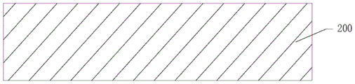
in step S1, a first conductive type substrate 200 (e.g., an N-type substrate) is provided, and the first conductive type substrate 200 has a front surface and a back surface opposite to the front surface, as shown in fig. 3.
In a preferred embodiment of the present invention, the thickness of the first conductive type substrate 200 is 350-600 μm (e.g., 350 μm, 400 μm, 500 μm, 600 μm, etc.).
Step S2, etching the first conductive type substrate 200 from the front surface of the first conductive type substrate 200 to form a plurality of first deep trenches 201, such as the structure shown in fig. 4; and the first deep trenches 201 are filled with a second conductive type silicon layer 202 (e.g., P-type silicon layer), as shown in fig. 5.
In a preferred embodiment of the present invention, the height of the first deep trench 201 is 50-60 μm (e.g., 50 μm, 52 μm, 55 μm, or 60 μm).
In step S3, a second conductive type epitaxial layer 203 (e.g., P-type epitaxial layer) is formed to cover the upper surfaces of the first conductive type substrate 200 and the second conductive type silicon layer 202, as shown in fig. 6.
In a preferred embodiment of the present invention, the thickness of the second conductive type epitaxial layer 203 is 10-50 μm (e.g., 10 μm, 20 μm, 25 μm, or 50 μm, etc.).
In step S4, an ion implantation process is performed on the second conductive type epitaxial layer 203 to form a first conductive type emitter region 204 (e.g., an N + emitter region) on the second conductive type epitaxial layer 203, as shown in fig. 7.
In a preferred embodiment of the present invention, the step S4 specifically includes: after the photolithography process, an ion implantation process is performed on the second conductive type epitaxial layer 203, and after thermal diffusion, a first conductive type emitter region 204 is formed on the upper portion of the second conductive type epitaxial layer 203.
Step S5, the second conductive type epitaxial layer 203 is partially etched and stopped in the first conductive type substrate 200 to form a second deep trench 205, and a conductive layer 207 is formed in the second deep trench 205, as shown in fig. 8-10.
In a preferred embodiment of the present invention, the step S5 specifically includes:
in step S51, the second conductive type epitaxial layer 203 is partially etched and stopped in the first conductive type substrate 200 to form a second deep trench 205, as shown in fig. 8.
In step S52, an isolation layer (thermal oxide isolation layer) 206 is prepared to cover the bottom and the sidewall of the second deep trench 205, and preferably, the isolation layer 206 is an oxide layer, as shown in fig. 9.
In step S53, the conductive layer 207 is formed in the second deep trench 205, preferably, the conductive layer 207 is polysilicon, as shown in fig. 10.
In step S6, a passivation layer 208 is prepared to cover the upper surfaces of second conductivity type epitaxial layer 203 and conductive layer 207, as in the structure shown in fig. 11.
Step S7, after etching (etching by photolithography process) the passivation layer 208 to form a first contact hole 209 exposing a portion of the upper surface of the second conductive type epitaxial layer 203 and a second contact hole 210 exposing the upper surface of the first conductive type emitter region 204, the structure shown in fig. 12 is obtained; the first contact 209 and the second contact 210 are filled with metal to form a gate 211 and a cathode 212, as shown in fig. 13.
In a preferred embodiment of the present invention, the first conductive type is N-type, the second conductive type is P-type, or the first conductive type is P-type, and the second conductive type is N-type.
Step S8, after performing a thinning process on the first conductive type substrate 200 from the back side, the structure shown in fig. 14 is obtained; the ion implantation process is continued on the first conductive type substrate 200 from the back side to form a second conductive type doped region 213 (the second conductive type doped region 213 is a second conductive type anode layer, for example, the implanted ions are boron ions, and then are a P-type anode layer), and the second conductive type doped region 213 contacts with the lower surface of the second conductive type silicon layer 202, as shown in fig. 15.
In a preferred embodiment of the present invention, the step S8 is specifically: first, a thinning process is performed on the first conductive type substrate 200 from the back side of the first conductive type substrate 200 to thin the first conductive type substrate 200 to 60-250 μm (for example, 60 μm, 100 μm, 200 μm, or 250 μm, etc.), then, an ion implantation process is performed on the first conductive type substrate 200 from the back side, and then, the implanted ions are activated by low temperature annealing or laser activation to form the second conductive type doped region 213, and the second conductive type doped region 213 is in contact with the lower surface of the second conductive type silicon layer 202.
In step S9, the back electrode 214 is prepared to cover the bottom surface of the second-conductivity-type-doped region 213, as shown in fig. 16.
It should be understood that this embodiment is a method embodiment corresponding to the above-mentioned embodiment of the thyristor device, and this embodiment may be implemented in cooperation with the above-mentioned embodiment of the thyristor device. The related technical details mentioned in the above embodiments of the silicon controlled device are still valid in this embodiment, and are not described herein again in order to reduce repetition. Accordingly, the related art details mentioned in the present embodiment can also be applied to the above-described embodiments of the thyristor device.
In summary, the invention discloses a silicon controlled device and a preparation method thereof, and compared with the long-time aluminum diffusion, mesa corrosion, glass passivation and other technologies adopted by the traditional technology, the silicon controlled device can reduce the area of the device and improve the consistency and yield of the device by adopting the modern technology such as deep groove etching, epitaxy and the like. The novel method adopts the modern conventional process module technology, so that the silicon controlled device can realize the collinear production with the integrated circuit chip and other power devices (such as power MOSFET and IGBT), and the flexible manufacturing capability of the modern chip production line of 8 inches or more is improved.
Those skilled in the art will appreciate that variations may be implemented by those skilled in the art in combination with the prior art and the above-described embodiments, and will not be described herein in detail. Such variations do not affect the essence of the present invention and are not described herein.
The above description is of the preferred embodiment of the invention. It is to be understood that the invention is not limited to the particular embodiments described above, in that devices and structures not described in detail are understood to be implemented in a manner common in the art; those skilled in the art can make many possible variations and modifications to the disclosed embodiments, or modify equivalent embodiments to equivalent variations, without departing from the spirit of the invention, using the methods and techniques disclosed above. Therefore, any simple modification, equivalent change and modification made to the above embodiments according to the technical essence of the present invention are still within the scope of the protection of the technical solution of the present invention, unless the contents of the technical solution of the present invention are departed.