CN108133687B - Pixel and organic light emitting display device having the same - Google Patents
Pixel and organic light emitting display device having the same Download PDFInfo
- Publication number
- CN108133687B CN108133687B CN201711193768.5A CN201711193768A CN108133687B CN 108133687 B CN108133687 B CN 108133687B CN 201711193768 A CN201711193768 A CN 201711193768A CN 108133687 B CN108133687 B CN 108133687B
- Authority
- CN
- China
- Prior art keywords
- transistor
- pixel
- coupled
- voltage
- node
- Prior art date
- Legal status (The legal status is an assumption and is not a legal conclusion. Google has not performed a legal analysis and makes no representation as to the accuracy of the status listed.)
- Active
Links
- 230000006641 stabilisation Effects 0.000 claims abstract description 215
- 238000011105 stabilization Methods 0.000 claims abstract description 215
- 239000003990 capacitor Substances 0.000 claims abstract description 71
- 239000004065 semiconductor Substances 0.000 claims description 165
- 229910021420 polycrystalline silicon Inorganic materials 0.000 claims description 79
- 229920005591 polysilicon Polymers 0.000 claims description 39
- 230000000087 stabilizing effect Effects 0.000 claims description 34
- 238000000034 method Methods 0.000 description 42
- 229910013756 M(PN) Inorganic materials 0.000 description 16
- 229910013763 M(PP) Inorganic materials 0.000 description 16
- 230000008878 coupling Effects 0.000 description 4
- 238000010168 coupling process Methods 0.000 description 4
- 238000005859 coupling reaction Methods 0.000 description 4
- 230000006870 function Effects 0.000 description 2
- 230000007274 generation of a signal involved in cell-cell signaling Effects 0.000 description 2
- 238000005070 sampling Methods 0.000 description 2
- 239000000758 substrate Substances 0.000 description 2
- 230000002411 adverse Effects 0.000 description 1
- 238000003491 array Methods 0.000 description 1
- 239000004973 liquid crystal related substance Substances 0.000 description 1
- 230000003071 parasitic effect Effects 0.000 description 1
- 230000004044 response Effects 0.000 description 1
- 230000001360 synchronised effect Effects 0.000 description 1
Images


Classifications
-
- G—PHYSICS
- G09—EDUCATION; CRYPTOGRAPHY; DISPLAY; ADVERTISING; SEALS
- G09G—ARRANGEMENTS OR CIRCUITS FOR CONTROL OF INDICATING DEVICES USING STATIC MEANS TO PRESENT VARIABLE INFORMATION
- G09G3/00—Control arrangements or circuits, of interest only in connection with visual indicators other than cathode-ray tubes
- G09G3/20—Control arrangements or circuits, of interest only in connection with visual indicators other than cathode-ray tubes for presentation of an assembly of a number of characters, e.g. a page, by composing the assembly by combination of individual elements arranged in a matrix no fixed position being assigned to or needed to be assigned to the individual characters or partial characters
- G09G3/22—Control arrangements or circuits, of interest only in connection with visual indicators other than cathode-ray tubes for presentation of an assembly of a number of characters, e.g. a page, by composing the assembly by combination of individual elements arranged in a matrix no fixed position being assigned to or needed to be assigned to the individual characters or partial characters using controlled light sources
- G09G3/30—Control arrangements or circuits, of interest only in connection with visual indicators other than cathode-ray tubes for presentation of an assembly of a number of characters, e.g. a page, by composing the assembly by combination of individual elements arranged in a matrix no fixed position being assigned to or needed to be assigned to the individual characters or partial characters using controlled light sources using electroluminescent panels
- G09G3/32—Control arrangements or circuits, of interest only in connection with visual indicators other than cathode-ray tubes for presentation of an assembly of a number of characters, e.g. a page, by composing the assembly by combination of individual elements arranged in a matrix no fixed position being assigned to or needed to be assigned to the individual characters or partial characters using controlled light sources using electroluminescent panels semiconductive, e.g. using light-emitting diodes [LED]
- G09G3/3208—Control arrangements or circuits, of interest only in connection with visual indicators other than cathode-ray tubes for presentation of an assembly of a number of characters, e.g. a page, by composing the assembly by combination of individual elements arranged in a matrix no fixed position being assigned to or needed to be assigned to the individual characters or partial characters using controlled light sources using electroluminescent panels semiconductive, e.g. using light-emitting diodes [LED] organic, e.g. using organic light-emitting diodes [OLED]
- G09G3/3225—Control arrangements or circuits, of interest only in connection with visual indicators other than cathode-ray tubes for presentation of an assembly of a number of characters, e.g. a page, by composing the assembly by combination of individual elements arranged in a matrix no fixed position being assigned to or needed to be assigned to the individual characters or partial characters using controlled light sources using electroluminescent panels semiconductive, e.g. using light-emitting diodes [LED] organic, e.g. using organic light-emitting diodes [OLED] using an active matrix
- G09G3/3233—Control arrangements or circuits, of interest only in connection with visual indicators other than cathode-ray tubes for presentation of an assembly of a number of characters, e.g. a page, by composing the assembly by combination of individual elements arranged in a matrix no fixed position being assigned to or needed to be assigned to the individual characters or partial characters using controlled light sources using electroluminescent panels semiconductive, e.g. using light-emitting diodes [LED] organic, e.g. using organic light-emitting diodes [OLED] using an active matrix with pixel circuitry controlling the current through the light-emitting element
-
- G—PHYSICS
- G09—EDUCATION; CRYPTOGRAPHY; DISPLAY; ADVERTISING; SEALS
- G09G—ARRANGEMENTS OR CIRCUITS FOR CONTROL OF INDICATING DEVICES USING STATIC MEANS TO PRESENT VARIABLE INFORMATION
- G09G3/00—Control arrangements or circuits, of interest only in connection with visual indicators other than cathode-ray tubes
- G09G3/20—Control arrangements or circuits, of interest only in connection with visual indicators other than cathode-ray tubes for presentation of an assembly of a number of characters, e.g. a page, by composing the assembly by combination of individual elements arranged in a matrix no fixed position being assigned to or needed to be assigned to the individual characters or partial characters
- G09G3/22—Control arrangements or circuits, of interest only in connection with visual indicators other than cathode-ray tubes for presentation of an assembly of a number of characters, e.g. a page, by composing the assembly by combination of individual elements arranged in a matrix no fixed position being assigned to or needed to be assigned to the individual characters or partial characters using controlled light sources
- G09G3/30—Control arrangements or circuits, of interest only in connection with visual indicators other than cathode-ray tubes for presentation of an assembly of a number of characters, e.g. a page, by composing the assembly by combination of individual elements arranged in a matrix no fixed position being assigned to or needed to be assigned to the individual characters or partial characters using controlled light sources using electroluminescent panels
- G09G3/32—Control arrangements or circuits, of interest only in connection with visual indicators other than cathode-ray tubes for presentation of an assembly of a number of characters, e.g. a page, by composing the assembly by combination of individual elements arranged in a matrix no fixed position being assigned to or needed to be assigned to the individual characters or partial characters using controlled light sources using electroluminescent panels semiconductive, e.g. using light-emitting diodes [LED]
- G09G3/3208—Control arrangements or circuits, of interest only in connection with visual indicators other than cathode-ray tubes for presentation of an assembly of a number of characters, e.g. a page, by composing the assembly by combination of individual elements arranged in a matrix no fixed position being assigned to or needed to be assigned to the individual characters or partial characters using controlled light sources using electroluminescent panels semiconductive, e.g. using light-emitting diodes [LED] organic, e.g. using organic light-emitting diodes [OLED]
- G09G3/3225—Control arrangements or circuits, of interest only in connection with visual indicators other than cathode-ray tubes for presentation of an assembly of a number of characters, e.g. a page, by composing the assembly by combination of individual elements arranged in a matrix no fixed position being assigned to or needed to be assigned to the individual characters or partial characters using controlled light sources using electroluminescent panels semiconductive, e.g. using light-emitting diodes [LED] organic, e.g. using organic light-emitting diodes [OLED] using an active matrix
- G09G3/3258—Control arrangements or circuits, of interest only in connection with visual indicators other than cathode-ray tubes for presentation of an assembly of a number of characters, e.g. a page, by composing the assembly by combination of individual elements arranged in a matrix no fixed position being assigned to or needed to be assigned to the individual characters or partial characters using controlled light sources using electroluminescent panels semiconductive, e.g. using light-emitting diodes [LED] organic, e.g. using organic light-emitting diodes [OLED] using an active matrix with pixel circuitry controlling the voltage across the light-emitting element
-
- G—PHYSICS
- G09—EDUCATION; CRYPTOGRAPHY; DISPLAY; ADVERTISING; SEALS
- G09G—ARRANGEMENTS OR CIRCUITS FOR CONTROL OF INDICATING DEVICES USING STATIC MEANS TO PRESENT VARIABLE INFORMATION
- G09G2300/00—Aspects of the constitution of display devices
- G09G2300/04—Structural and physical details of display devices
- G09G2300/0421—Structural details of the set of electrodes
- G09G2300/0426—Layout of electrodes and connections
-
- G—PHYSICS
- G09—EDUCATION; CRYPTOGRAPHY; DISPLAY; ADVERTISING; SEALS
- G09G—ARRANGEMENTS OR CIRCUITS FOR CONTROL OF INDICATING DEVICES USING STATIC MEANS TO PRESENT VARIABLE INFORMATION
- G09G2300/00—Aspects of the constitution of display devices
- G09G2300/08—Active matrix structure, i.e. with use of active elements, inclusive of non-linear two terminal elements, in the pixels together with light emitting or modulating elements
- G09G2300/0809—Several active elements per pixel in active matrix panels
- G09G2300/0819—Several active elements per pixel in active matrix panels used for counteracting undesired variations, e.g. feedback or autozeroing
-
- G—PHYSICS
- G09—EDUCATION; CRYPTOGRAPHY; DISPLAY; ADVERTISING; SEALS
- G09G—ARRANGEMENTS OR CIRCUITS FOR CONTROL OF INDICATING DEVICES USING STATIC MEANS TO PRESENT VARIABLE INFORMATION
- G09G2300/00—Aspects of the constitution of display devices
- G09G2300/08—Active matrix structure, i.e. with use of active elements, inclusive of non-linear two terminal elements, in the pixels together with light emitting or modulating elements
- G09G2300/0809—Several active elements per pixel in active matrix panels
- G09G2300/0842—Several active elements per pixel in active matrix panels forming a memory circuit, e.g. a dynamic memory with one capacitor
- G09G2300/0852—Several active elements per pixel in active matrix panels forming a memory circuit, e.g. a dynamic memory with one capacitor being a dynamic memory with more than one capacitor
-
- G—PHYSICS
- G09—EDUCATION; CRYPTOGRAPHY; DISPLAY; ADVERTISING; SEALS
- G09G—ARRANGEMENTS OR CIRCUITS FOR CONTROL OF INDICATING DEVICES USING STATIC MEANS TO PRESENT VARIABLE INFORMATION
- G09G2310/00—Command of the display device
- G09G2310/02—Addressing, scanning or driving the display screen or processing steps related thereto
- G09G2310/0202—Addressing of scan or signal lines
- G09G2310/0216—Interleaved control phases for different scan lines in the same sub-field, e.g. initialization, addressing and sustaining in plasma displays that are not simultaneous for all scan lines
-
- G—PHYSICS
- G09—EDUCATION; CRYPTOGRAPHY; DISPLAY; ADVERTISING; SEALS
- G09G—ARRANGEMENTS OR CIRCUITS FOR CONTROL OF INDICATING DEVICES USING STATIC MEANS TO PRESENT VARIABLE INFORMATION
- G09G2310/00—Command of the display device
- G09G2310/08—Details of timing specific for flat panels, other than clock recovery
-
- G—PHYSICS
- G09—EDUCATION; CRYPTOGRAPHY; DISPLAY; ADVERTISING; SEALS
- G09G—ARRANGEMENTS OR CIRCUITS FOR CONTROL OF INDICATING DEVICES USING STATIC MEANS TO PRESENT VARIABLE INFORMATION
- G09G2320/00—Control of display operating conditions
- G09G2320/02—Improving the quality of display appearance
- G09G2320/0209—Crosstalk reduction, i.e. to reduce direct or indirect influences of signals directed to a certain pixel of the displayed image on other pixels of said image, inclusive of influences affecting pixels in different frames or fields or sub-images which constitute a same image, e.g. left and right images of a stereoscopic display
- G09G2320/0214—Crosstalk reduction, i.e. to reduce direct or indirect influences of signals directed to a certain pixel of the displayed image on other pixels of said image, inclusive of influences affecting pixels in different frames or fields or sub-images which constitute a same image, e.g. left and right images of a stereoscopic display with crosstalk due to leakage current of pixel switch in active matrix panels
-
- G—PHYSICS
- G09—EDUCATION; CRYPTOGRAPHY; DISPLAY; ADVERTISING; SEALS
- G09G—ARRANGEMENTS OR CIRCUITS FOR CONTROL OF INDICATING DEVICES USING STATIC MEANS TO PRESENT VARIABLE INFORMATION
- G09G2320/00—Control of display operating conditions
- G09G2320/04—Maintaining the quality of display appearance
- G09G2320/043—Preventing or counteracting the effects of ageing
- G09G2320/045—Compensation of drifts in the characteristics of light emitting or modulating elements
-
- G—PHYSICS
- G09—EDUCATION; CRYPTOGRAPHY; DISPLAY; ADVERTISING; SEALS
- G09G—ARRANGEMENTS OR CIRCUITS FOR CONTROL OF INDICATING DEVICES USING STATIC MEANS TO PRESENT VARIABLE INFORMATION
- G09G2320/00—Control of display operating conditions
- G09G2320/06—Adjustment of display parameters
- G09G2320/0626—Adjustment of display parameters for control of overall brightness
-
- G—PHYSICS
- G09—EDUCATION; CRYPTOGRAPHY; DISPLAY; ADVERTISING; SEALS
- G09G—ARRANGEMENTS OR CIRCUITS FOR CONTROL OF INDICATING DEVICES USING STATIC MEANS TO PRESENT VARIABLE INFORMATION
- G09G2330/00—Aspects of power supply; Aspects of display protection and defect management
- G09G2330/02—Details of power systems and of start or stop of display operation
- G09G2330/021—Power management, e.g. power saving
- G09G2330/023—Power management, e.g. power saving using energy recovery or conservation
-
- G—PHYSICS
- G09—EDUCATION; CRYPTOGRAPHY; DISPLAY; ADVERTISING; SEALS
- G09G—ARRANGEMENTS OR CIRCUITS FOR CONTROL OF INDICATING DEVICES USING STATIC MEANS TO PRESENT VARIABLE INFORMATION
- G09G3/00—Control arrangements or circuits, of interest only in connection with visual indicators other than cathode-ray tubes
- G09G3/20—Control arrangements or circuits, of interest only in connection with visual indicators other than cathode-ray tubes for presentation of an assembly of a number of characters, e.g. a page, by composing the assembly by combination of individual elements arranged in a matrix no fixed position being assigned to or needed to be assigned to the individual characters or partial characters
- G09G3/22—Control arrangements or circuits, of interest only in connection with visual indicators other than cathode-ray tubes for presentation of an assembly of a number of characters, e.g. a page, by composing the assembly by combination of individual elements arranged in a matrix no fixed position being assigned to or needed to be assigned to the individual characters or partial characters using controlled light sources
- G09G3/30—Control arrangements or circuits, of interest only in connection with visual indicators other than cathode-ray tubes for presentation of an assembly of a number of characters, e.g. a page, by composing the assembly by combination of individual elements arranged in a matrix no fixed position being assigned to or needed to be assigned to the individual characters or partial characters using controlled light sources using electroluminescent panels
- G09G3/32—Control arrangements or circuits, of interest only in connection with visual indicators other than cathode-ray tubes for presentation of an assembly of a number of characters, e.g. a page, by composing the assembly by combination of individual elements arranged in a matrix no fixed position being assigned to or needed to be assigned to the individual characters or partial characters using controlled light sources using electroluminescent panels semiconductive, e.g. using light-emitting diodes [LED]
- G09G3/3208—Control arrangements or circuits, of interest only in connection with visual indicators other than cathode-ray tubes for presentation of an assembly of a number of characters, e.g. a page, by composing the assembly by combination of individual elements arranged in a matrix no fixed position being assigned to or needed to be assigned to the individual characters or partial characters using controlled light sources using electroluminescent panels semiconductive, e.g. using light-emitting diodes [LED] organic, e.g. using organic light-emitting diodes [OLED]
- G09G3/3266—Details of drivers for scan electrodes
-
- G—PHYSICS
- G09—EDUCATION; CRYPTOGRAPHY; DISPLAY; ADVERTISING; SEALS
- G09G—ARRANGEMENTS OR CIRCUITS FOR CONTROL OF INDICATING DEVICES USING STATIC MEANS TO PRESENT VARIABLE INFORMATION
- G09G3/00—Control arrangements or circuits, of interest only in connection with visual indicators other than cathode-ray tubes
- G09G3/20—Control arrangements or circuits, of interest only in connection with visual indicators other than cathode-ray tubes for presentation of an assembly of a number of characters, e.g. a page, by composing the assembly by combination of individual elements arranged in a matrix no fixed position being assigned to or needed to be assigned to the individual characters or partial characters
- G09G3/22—Control arrangements or circuits, of interest only in connection with visual indicators other than cathode-ray tubes for presentation of an assembly of a number of characters, e.g. a page, by composing the assembly by combination of individual elements arranged in a matrix no fixed position being assigned to or needed to be assigned to the individual characters or partial characters using controlled light sources
- G09G3/30—Control arrangements or circuits, of interest only in connection with visual indicators other than cathode-ray tubes for presentation of an assembly of a number of characters, e.g. a page, by composing the assembly by combination of individual elements arranged in a matrix no fixed position being assigned to or needed to be assigned to the individual characters or partial characters using controlled light sources using electroluminescent panels
- G09G3/32—Control arrangements or circuits, of interest only in connection with visual indicators other than cathode-ray tubes for presentation of an assembly of a number of characters, e.g. a page, by composing the assembly by combination of individual elements arranged in a matrix no fixed position being assigned to or needed to be assigned to the individual characters or partial characters using controlled light sources using electroluminescent panels semiconductive, e.g. using light-emitting diodes [LED]
- G09G3/3208—Control arrangements or circuits, of interest only in connection with visual indicators other than cathode-ray tubes for presentation of an assembly of a number of characters, e.g. a page, by composing the assembly by combination of individual elements arranged in a matrix no fixed position being assigned to or needed to be assigned to the individual characters or partial characters using controlled light sources using electroluminescent panels semiconductive, e.g. using light-emitting diodes [LED] organic, e.g. using organic light-emitting diodes [OLED]
- G09G3/3275—Details of drivers for data electrodes
-
- G—PHYSICS
- G09—EDUCATION; CRYPTOGRAPHY; DISPLAY; ADVERTISING; SEALS
- G09G—ARRANGEMENTS OR CIRCUITS FOR CONTROL OF INDICATING DEVICES USING STATIC MEANS TO PRESENT VARIABLE INFORMATION
- G09G3/00—Control arrangements or circuits, of interest only in connection with visual indicators other than cathode-ray tubes
- G09G3/20—Control arrangements or circuits, of interest only in connection with visual indicators other than cathode-ray tubes for presentation of an assembly of a number of characters, e.g. a page, by composing the assembly by combination of individual elements arranged in a matrix no fixed position being assigned to or needed to be assigned to the individual characters or partial characters
- G09G3/34—Control arrangements or circuits, of interest only in connection with visual indicators other than cathode-ray tubes for presentation of an assembly of a number of characters, e.g. a page, by composing the assembly by combination of individual elements arranged in a matrix no fixed position being assigned to or needed to be assigned to the individual characters or partial characters by control of light from an independent source
- G09G3/36—Control arrangements or circuits, of interest only in connection with visual indicators other than cathode-ray tubes for presentation of an assembly of a number of characters, e.g. a page, by composing the assembly by combination of individual elements arranged in a matrix no fixed position being assigned to or needed to be assigned to the individual characters or partial characters by control of light from an independent source using liquid crystals
- G09G3/3611—Control of matrices with row and column drivers
- G09G3/3648—Control of matrices with row and column drivers using an active matrix
-
- H—ELECTRICITY
- H10—SEMICONDUCTOR DEVICES; ELECTRIC SOLID-STATE DEVICES NOT OTHERWISE PROVIDED FOR
- H10D—INORGANIC ELECTRIC SEMICONDUCTOR DEVICES
- H10D30/00—Field-effect transistors [FET]
- H10D30/60—Insulated-gate field-effect transistors [IGFET]
- H10D30/67—Thin-film transistors [TFT]
- H10D30/674—Thin-film transistors [TFT] characterised by the active materials
- H10D30/6741—Group IV materials, e.g. germanium or silicon carbide
- H10D30/6743—Silicon
- H10D30/6745—Polycrystalline or microcrystalline silicon
-
- H—ELECTRICITY
- H10—SEMICONDUCTOR DEVICES; ELECTRIC SOLID-STATE DEVICES NOT OTHERWISE PROVIDED FOR
- H10D—INORGANIC ELECTRIC SEMICONDUCTOR DEVICES
- H10D30/00—Field-effect transistors [FET]
- H10D30/60—Insulated-gate field-effect transistors [IGFET]
- H10D30/67—Thin-film transistors [TFT]
- H10D30/674—Thin-film transistors [TFT] characterised by the active materials
- H10D30/6755—Oxide semiconductors, e.g. zinc oxide, copper aluminium oxide or cadmium stannate
-
- H—ELECTRICITY
- H10—SEMICONDUCTOR DEVICES; ELECTRIC SOLID-STATE DEVICES NOT OTHERWISE PROVIDED FOR
- H10D—INORGANIC ELECTRIC SEMICONDUCTOR DEVICES
- H10D86/00—Integrated devices formed in or on insulating or conducting substrates, e.g. formed in silicon-on-insulator [SOI] substrates or on stainless steel or glass substrates
- H10D86/40—Integrated devices formed in or on insulating or conducting substrates, e.g. formed in silicon-on-insulator [SOI] substrates or on stainless steel or glass substrates characterised by multiple TFTs
- H10D86/421—Integrated devices formed in or on insulating or conducting substrates, e.g. formed in silicon-on-insulator [SOI] substrates or on stainless steel or glass substrates characterised by multiple TFTs having a particular composition, shape or crystalline structure of the active layer
- H10D86/423—Integrated devices formed in or on insulating or conducting substrates, e.g. formed in silicon-on-insulator [SOI] substrates or on stainless steel or glass substrates characterised by multiple TFTs having a particular composition, shape or crystalline structure of the active layer comprising semiconductor materials not belonging to the Group IV, e.g. InGaZnO
-
- H—ELECTRICITY
- H10—SEMICONDUCTOR DEVICES; ELECTRIC SOLID-STATE DEVICES NOT OTHERWISE PROVIDED FOR
- H10D—INORGANIC ELECTRIC SEMICONDUCTOR DEVICES
- H10D86/00—Integrated devices formed in or on insulating or conducting substrates, e.g. formed in silicon-on-insulator [SOI] substrates or on stainless steel or glass substrates
- H10D86/40—Integrated devices formed in or on insulating or conducting substrates, e.g. formed in silicon-on-insulator [SOI] substrates or on stainless steel or glass substrates characterised by multiple TFTs
- H10D86/60—Integrated devices formed in or on insulating or conducting substrates, e.g. formed in silicon-on-insulator [SOI] substrates or on stainless steel or glass substrates characterised by multiple TFTs wherein the TFTs are in active matrices
Landscapes
- Engineering & Computer Science (AREA)
- Physics & Mathematics (AREA)
- Computer Hardware Design (AREA)
- General Physics & Mathematics (AREA)
- Theoretical Computer Science (AREA)
- Electroluminescent Light Sources (AREA)
- Control Of Indicators Other Than Cathode Ray Tubes (AREA)
- Control Of El Displays (AREA)
Abstract
Description
于2016年12月1日提交的第10-2016-0162995号、名称为“像素和具有该像素的有机发光显示装置(Pixel and Organic Light Emitting Display Device Having thePixel)”的韩国专利申请通过引用全部包含于此。Korean Patent Application No. 10-2016-0162995, filed on December 1, 2016, entitled "Pixel and Organic Light Emitting Display Device Having the Pixel", is incorporated by reference in its entirety here.
技术领域technical field
在此描述的一个或更多个实施例涉及有机发光显示装置和在这样的装置中的像素。One or more embodiments described herein relate to organic light emitting display devices and pixels in such devices.
背景技术Background technique
已经开发了各种显示器。示例包括液晶显示器和有机发光显示器。有机发光显示器基于从包括有机发光二极管的像素发射的光产生图像。有机发光显示器具有高响应速度和低功耗。Various displays have been developed. Examples include liquid crystal displays and organic light emitting displays. Organic light emitting displays generate images based on light emitted from pixels including organic light emitting diodes. Organic light-emitting displays have high response speed and low power consumption.
在有机发光显示器中,数据线和扫描线运载用于驱动像素的信号。像素具有控制流经相应的有机发光二极管的电流的量的驱动晶体管。具体地,每个驱动晶体管基于数据信号控制从第一驱动电源经由有机发光二极管流动到第二驱动电源的电流的量。发射与来自驱动晶体管的电流的量对应的具有预定的亮度的光。In an organic light emitting display, data lines and scan lines carry signals for driving pixels. The pixels have drive transistors that control the amount of current flowing through the corresponding organic light emitting diodes. Specifically, each driving transistor controls the amount of current flowing from the first driving power source to the second driving power source via the organic light emitting diode based on the data signal. Light having a predetermined brightness corresponding to the amount of current from the driving transistor is emitted.
已经提出在有机发光显示器中控制亮度的各种方法。一种方法涉及将第二驱动电源设定为低电压。另一方法涉及通过以低频率驱动显示器来减少功耗。然而,这些方法具有缺点,例如,会从像素驱动晶体管的栅电极产生预定的漏电流。因此,在一个帧时间段期间不保持数据信号的电压,反过来,这不利地影响亮度。Various methods of controlling brightness in organic light emitting displays have been proposed. One method involves setting the second drive power source to a low voltage. Another approach involves reducing power consumption by driving the display at low frequencies. However, these methods have disadvantages, for example, a predetermined leakage current is generated from the gate electrode of the pixel driving transistor. Therefore, the voltage of the data signal is not maintained during a frame period, which in turn adversely affects the brightness.
发明内容SUMMARY OF THE INVENTION
根据一个或更多个实施例,一种像素包括:有机发光二极管;第一晶体管,结合在结合到第一节点的第一驱动电源与有机发光二极管的阳极电极之间,第一晶体管基于第二节点的电压控制从第一驱动电源到有机发光二极管的电流的量;第二晶体管,结合在数据线与第一节点之间,当第一扫描信号供应到第i(i是自然数)第一扫描线时,第二晶体管导通;第三晶体管,结合在第一晶体管的第二电极与第二节点之间,当供应第一扫描信号时,第三晶体管导通;存储电容器,结合在第一驱动电源与第二节点之间;以及第一稳定化晶体管,结合在第三晶体管与第二节点之间或者第一晶体管的第二电极与第三晶体管之间,在第三晶体管截止的时间段的一部分期间,第一稳定化晶体管被设定为截止状态。第一晶体管、第二晶体管和第三晶体管可以是P型多晶硅半导体晶体管。第一稳定化晶体管可以是N型氧化物半导体晶体管。According to one or more embodiments, a pixel includes: an organic light emitting diode; a first transistor coupled between a first driving power source coupled to a first node and an anode electrode of the organic light emitting diode, the first transistor based on a second The voltage of the node controls the amount of current from the first driving power supply to the organic light emitting diode; the second transistor, coupled between the data line and the first node, when the first scan signal is supplied to the i-th (i is a natural number) first scan line, the second transistor is turned on; the third transistor is connected between the second electrode of the first transistor and the second node, when the first scan signal is supplied, the third transistor is turned on; the storage capacitor is connected to the first between the driving power supply and the second node; and a first stabilization transistor coupled between the third transistor and the second node or between the second electrode of the first transistor and the third transistor, during a period when the third transistor is off During a part of the period, the first stabilization transistor is set to the OFF state. The first transistor, the second transistor and the third transistor may be P-type polysilicon semiconductor transistors. The first stabilization transistor may be an N-type oxide semiconductor transistor.
第一稳定化晶体管的栅电极可结合到控制电源,在以第一驱动频率驱动像素的时间段期间,控制电源可被设定为栅极导通电压,在以比第一驱动频率低的第二驱动频率驱动像素的时间段的一部分期间,控制电源可被设定为栅极截止电压。当以第二驱动频率驱动像素时,在数据信号的电压存储在存储电容器中之后,控制电源可被设定为栅极截止电压。The gate electrode of the first stabilizing transistor may be coupled to a control power supply, which may be set to a gate-on voltage during a period of time when the pixel is driven at the first driving frequency, at a second driving frequency lower than the first driving frequency. During a portion of the time period in which the pixel is driven at two drive frequencies, the control power supply may be set to the gate-off voltage. When the pixel is driven at the second driving frequency, after the voltage of the data signal is stored in the storage capacitor, the control power supply may be set to the gate-off voltage.
像素可包括:第六晶体管,结合在第一节点与第一驱动电源之间,当发光控制信号供应到第i发光控制线时,第六晶体管截止,当发光控制信号不供应到第i发光控制线时,第六晶体管导通;以及第七晶体管,结合在第一晶体管的第二电极与有机发光二极管的阳极电极之间,第七晶体管与第六晶体管同时地导通或截止,其中,供应到第i发光控制线的发光控制信号被设定为比第一扫描信号更宽的宽度,并被供应为与第一扫描信号重叠。第一稳定化晶体管的栅电极可结合到第i发光控制线。The pixel may include: a sixth transistor coupled between the first node and the first driving power supply, the sixth transistor is turned off when the light-emitting control signal is supplied to the i-th light-emitting control line, and is turned off when the light-emitting control signal is not supplied to the i-th light-emitting control line line, the sixth transistor is turned on; and the seventh transistor is coupled between the second electrode of the first transistor and the anode electrode of the organic light emitting diode, the seventh transistor and the sixth transistor are turned on or off simultaneously, wherein the supply The light emission control signal to the i-th light emission control line is set to have a wider width than the first scan signal, and is supplied to overlap the first scan signal. The gate electrode of the first stabilization transistor may be coupled to the i-th light emission control line.
像素可包括:第四晶体管,结合在第二节点与第一电源之间,当第二扫描信号供应到第i第二扫描线时,第四晶体管导通;以及第二稳定化晶体管,结合在第二节点与第四晶体管之间或者第四晶体管与第一电源之间,在第四晶体管截止的时间段的一部分期间,第二稳定化晶体管被设定为截止状态。第一电源可被设定为比供应到数据线的数据信号低的电压。第二稳定化晶体管可以是N型氧化物半导体晶体管。The pixel may include: a fourth transistor coupled between the second node and the first power source, the fourth transistor is turned on when the second scan signal is supplied to the i-th second scan line; and a second stabilization transistor coupled in Between the second node and the fourth transistor or between the fourth transistor and the first power supply, the second stabilizing transistor is set to an off state during a portion of the period in which the fourth transistor is off. The first power source may be set to a lower voltage than the data signal supplied to the data line. The second stabilization transistor may be an N-type oxide semiconductor transistor.
第二稳定化晶体管的栅电极可结合到控制电源,在以第一驱动频率驱动像素的时间段期间,控制电源可被设定为栅极导通电压,在以比第一驱动频率低的第二驱动频率驱动像素的时间段的一部分期间,控制电源被设定为栅极截止电压。当以第二驱动频率驱动像素时,在数据信号的电压存储在存储电容器中之后,控制电源可被设定为栅极截止电压。The gate electrode of the second stabilizing transistor may be coupled to a control power supply, which may be set to the gate-on voltage during the time period when the pixel is driven at the first driving frequency, at a second driving frequency lower than the first driving frequency. During a portion of the time period in which the pixel is driven at two drive frequencies, the control power supply is set to the gate-off voltage. When the pixel is driven at the second driving frequency, after the voltage of the data signal is stored in the storage capacitor, the control power supply may be set to the gate-off voltage.
像素可包括:第六晶体管,结合在第一节点与第一驱动电源之间,当发光控制信号供应到第i发光控制线时,第六晶体管截止,反之,第六晶体管则导通;以及第七晶体管,结合在第一晶体管的第二电极与有机发光二极管的阳极电极之间,第七晶体管与第六晶体管同时地导通或截止,其中,供应到第i发光控制线的发光控制信号被设定为比第一扫描信号更宽的宽度,并被供应为与第一扫描信号重叠。第二稳定化晶体管的栅电极可结合到第i发光控制线。第i第二扫描线可被设定为第i-1第一扫描线。The pixel may include: a sixth transistor coupled between the first node and the first driving power supply, when the light-emitting control signal is supplied to the i-th light-emitting control line, the sixth transistor is turned off, otherwise, the sixth transistor is turned on; and Seven transistors are combined between the second electrode of the first transistor and the anode electrode of the organic light emitting diode, the seventh transistor is turned on or off simultaneously with the sixth transistor, wherein the light emitting control signal supplied to the i-th light emitting control line is It is set to a wider width than the first scan signal, and is supplied to overlap with the first scan signal. The gate electrode of the second stabilization transistor may be coupled to the i-th light emission control line. The i-th second scan line may be set as the i-1-th first scan line.
像素可包括:第五晶体管,结合在有机发光二极管的阳极电极与第一电源之间,当第三扫描信号供应到第i第三扫描线时,第五晶体管导通;以及第三稳定化晶体管,结合在有机发光二极管的阳极电极与第五晶体管之间或者第五晶体管与第一电源之间,在第五晶体管截止的时间段的一部分期间,第三稳定化晶体管被设定为截止状态。第三稳定化晶体管可以是N型氧化物半导体晶体管。The pixel may include: a fifth transistor coupled between the anode electrode of the organic light emitting diode and the first power source, the fifth transistor is turned on when the third scan signal is supplied to the i-th third scan line; and a third stabilization transistor , coupled between the anode electrode of the organic light emitting diode and the fifth transistor or between the fifth transistor and the first power source, the third stabilizing transistor is set to an off state during a portion of the period in which the fifth transistor is off. The third stabilization transistor may be an N-type oxide semiconductor transistor.
第三稳定化晶体管的栅电极可结合到控制电源,在以第一驱动频率驱动像素的时间段期间,控制电源可被设定为栅极导通电压,在以比第一驱动频率低的第二驱动频率驱动像素的时间段的一部分期间,控制电源可被设定为栅极截止电压。当以第二驱动频率驱动像素时,在数据信号的电压存储在存储电容器中之后,控制电源可被设定为栅极截止电压。The gate electrode of the third stabilizing transistor may be coupled to a control power supply, which may be set to the gate-on voltage during the period in which the pixel is driven at the first driving frequency, at a second driving frequency lower than the first driving frequency. During a portion of the time period in which the pixel is driven at two drive frequencies, the control power supply may be set to the gate-off voltage. When the pixel is driven at the second driving frequency, after the voltage of the data signal is stored in the storage capacitor, the control power supply may be set to the gate-off voltage.
像素可包括:第六晶体管,结合在第一节点与第一驱动电源之间,当发光控制信号供应到第i发光控制线时,第六晶体管截止,反之,第六晶体管则导通;以及第七晶体管,结合在第一晶体管的第二电极与有机发光二极管的阳极电极之间,第七晶体管与第六晶体管同时地导通或截止,其中,供应到第i发光控制线的发光控制信号被设定为比第一扫描信号更宽的宽度,并被供应为与第一扫描信号重叠。第三稳定化晶体管的栅电极可结合到第i发光控制线。第i第三扫描线可被设定为第i第一扫描线。The pixel may include: a sixth transistor coupled between the first node and the first driving power supply, when the light-emitting control signal is supplied to the i-th light-emitting control line, the sixth transistor is turned off, otherwise, the sixth transistor is turned on; and Seven transistors are combined between the second electrode of the first transistor and the anode electrode of the organic light emitting diode, the seventh transistor is turned on or off simultaneously with the sixth transistor, wherein the light emitting control signal supplied to the i-th light emitting control line is It is set to a wider width than the first scan signal, and is supplied to overlap with the first scan signal. The gate electrode of the third stabilization transistor may be coupled to the i-th light emission control line. The i-th third scan line may be set as the i-th first scan line.
根据一个或更多个其它实施例,一种像素包括:有机发光二极管;第一晶体管,基于第一节点的电压,控制从第一驱动电源经由有机发光二极管流动到第二驱动电源的电流的量;第二晶体管,结合在数据线与第一节点之间,当扫描信号供应到扫描线时,第二晶体管导通;存储电容器,结合在第一节点与第一晶体管的第二电极之间;以及稳定化晶体管,结合在数据线与第二晶体管之间或者第二晶体管与第一节点之间,其中,第一晶体管和第二晶体管是N型多晶硅半导体晶体管,稳定化晶体管是N型氧化物半导体晶体管。According to one or more other embodiments, a pixel includes: an organic light emitting diode; and a first transistor that controls an amount of current flowing from a first driving power source via the organic light emitting diode to a second driving power source based on a voltage of a first node The second transistor is combined between the data line and the first node, and when the scan signal is supplied to the scan line, the second transistor is turned on; the storage capacitor is combined between the first node and the second electrode of the first transistor; and a stabilization transistor, coupled between the data line and the second transistor or between the second transistor and the first node, wherein the first transistor and the second transistor are N-type polysilicon semiconductor transistors, and the stabilization transistor is an N-type oxide semiconductor transistors.
稳定化晶体管的栅电极可结合到控制电源,在以第一驱动频率驱动像素的时间段期间,控制电源可被设定为栅极导通电压,在以比第一驱动频率低的第二驱动频率驱动像素的时间段的一部分期间,控制电源可被设定为栅极截止电压。The gate electrode of the stabilizing transistor may be coupled to a control power supply that may be set to a gate-on voltage during periods of time driving the pixel at a first drive frequency, and may be set to a gate-on voltage during a period of time driving the pixel at a second drive frequency that is lower than the first drive frequency. The control power supply may be set to the gate-off voltage during a portion of the time period in which the pixel is driven at the frequency.
当以第二驱动频率驱动像素时,在数据信号的电压存储在存储电容器中之后,控制电源可被设定为栅极截止电压。稳定化晶体管的栅电极可结合到扫描线。像素可包括:第三晶体管,结合在第一驱动电源与第一晶体管的第一电极之间,第三晶体管具有不与第二晶体管重叠的导通时间段。When the pixel is driven at the second driving frequency, after the voltage of the data signal is stored in the storage capacitor, the control power supply may be set to the gate-off voltage. The gate electrodes of the stabilized transistors may be coupled to the scan lines. The pixel may include a third transistor coupled between the first driving power source and the first electrode of the first transistor, the third transistor having an on-time period that does not overlap with the second transistor.
根据一个或更多个其它实施例,一种像素包括:有机发光二极管;第一晶体管,基于第一节点的电压,控制从第一驱动电源经由有机发光二极管流动到第二驱动电源的电流的量;第二晶体管,结合在数据线与第二节点之间,当扫描信号供应到扫描线时,第二晶体管导通;第三晶体管,结合在第二节点与第一晶体管的第二电极之间,当发光控制信号供应到第i-1发光控制线时,第三晶体管截止;第四晶体管,结合在第一节点与第一晶体管的第一电极之间,当供应扫描信号时,第四晶体管导通;存储电容器,结合在第一节点与第二节点之间;以及第一稳定化晶体管,结合在第一节点与第四晶体管之间或者第四晶体管与第一晶体管的第一电极之间,其中,第一晶体管至第四晶体管是N型多晶硅半导体晶体管,第一稳定化晶体管是N型氧化物半导体晶体管。According to one or more other embodiments, a pixel includes: an organic light emitting diode; and a first transistor that controls an amount of current flowing from a first driving power source via the organic light emitting diode to a second driving power source based on a voltage of a first node The second transistor is combined between the data line and the second node, and when the scan signal is supplied to the scan line, the second transistor is turned on; the third transistor is combined between the second node and the second electrode of the first transistor , when the light-emitting control signal is supplied to the i-1th light-emitting control line, the third transistor is turned off; the fourth transistor is combined between the first node and the first electrode of the first transistor, and when the scan signal is supplied, the fourth transistor is turned off on; a storage capacitor coupled between the first node and the second node; and a first stabilization transistor coupled between the first node and the fourth transistor or between the fourth transistor and the first electrode of the first transistor , wherein the first to fourth transistors are N-type polysilicon semiconductor transistors, and the first stabilization transistor is an N-type oxide semiconductor transistor.
第一稳定化晶体管的栅电极可结合到控制电源,在以第一驱动频率驱动像素的时间段期间,控制电源可被设定为栅极导通电压,在以比第一驱动频率低的第二驱动频率驱动像素的时间段的一部分期间,控制电源可被设定为栅极截止电压。The gate electrode of the first stabilizing transistor may be coupled to a control power supply, which may be set to a gate-on voltage during a period of time when the pixel is driven at the first driving frequency, at a second driving frequency lower than the first driving frequency. During a portion of the time period in which the pixel is driven at two drive frequencies, the control power supply may be set to the gate-off voltage.
当以第二驱动频率驱动像素时,在数据信号的电压存储在存储电容器中之后,控制电源可被设定为栅极截止电压。第一稳定化晶体管的栅电极可结合到扫描线。像素可包括:第二稳定化晶体管,结合在数据线与第二晶体管之间或者第二晶体管与第二节点之间。第二稳定化晶体管可以是N型氧化物半导体晶体管。When the pixel is driven at the second driving frequency, after the voltage of the data signal is stored in the storage capacitor, the control power supply may be set to the gate-off voltage. The gate electrode of the first stabilization transistor may be coupled to the scan line. The pixel may include a second stabilization transistor coupled between the data line and the second transistor or between the second transistor and the second node. The second stabilization transistor may be an N-type oxide semiconductor transistor.
第二稳定化晶体管的栅电极结合到控制电源,在以第一驱动频率驱动像素的时间段期间,控制电源被设定为栅极导通电压,在以比第一驱动频率低的第二驱动频率驱动像素的时间段的一部分期间,控制电源被设定为栅极截止电压。当以第二驱动频率驱动像素时,在数据信号的电压存储在存储电容器中之后,控制电源可被设定为栅极截止电压。第二稳定化晶体管的栅电极可结合到扫描线。The gate electrode of the second stabilizing transistor is coupled to a control power supply, which is set to the gate-on voltage during the period in which the pixel is driven at the first drive frequency, at a second drive frequency that is lower than the first drive frequency. The control power supply is set to the gate-off voltage during a portion of the time period in which the pixel is driven at the frequency. When the pixel is driven at the second driving frequency, after the voltage of the data signal is stored in the storage capacitor, the control power supply may be set to the gate-off voltage. The gate electrode of the second stabilization transistor may be coupled to the scan line.
像素可包括:第五晶体管,结合在第一电源与有机发光二极管的阳极电极之间,第五晶体管具有结合到扫描线的栅电极;以及第六晶体管,结合在第一驱动电源与第一晶体管的第一电极之间,第六晶体管具有结合到第i发光控制线的栅电极。The pixel may include: a fifth transistor coupled between the first power source and the anode electrode of the organic light emitting diode, the fifth transistor having a gate electrode coupled to the scan line; and a sixth transistor coupled between the first driving power source and the first transistor Between the first electrodes of the sixth transistor, the sixth transistor has a gate electrode coupled to the i-th light-emitting control line.
根据一个或更多个其它实施例,一种像素包括:有机发光二极管;第一晶体管,基于第一节点的电压,控制从第一驱动电源经由有机发光二极管流动到第二驱动电源的电流的量;第二晶体管,结合在第一电源与有机发光二极管的阳极电极之间,当第二扫描信号供应到第二扫描线时,第二晶体管导通;第三晶体管,结合在第一节点与第一晶体管的第二电极之间,当第一扫描信号供应到第一扫描线时,第三晶体管导通;存储电容器,结合在第一电源与第一节点之间;以及第一稳定化晶体管,结合在第一节点与第三晶体管之间或者第三晶体管与第一晶体管的第二电极之间,其中,第一晶体管至第三晶体管是N型多晶硅半导体晶体管,第一稳定化晶体管是N型氧化物半导体晶体管。According to one or more other embodiments, a pixel includes: an organic light emitting diode; and a first transistor that controls an amount of current flowing from a first driving power source via the organic light emitting diode to a second driving power source based on a voltage of a first node The second transistor is connected between the first power supply and the anode electrode of the organic light emitting diode, when the second scan signal is supplied to the second scan line, the second transistor is turned on; the third transistor is connected between the first node and the first node Between the second electrodes of a transistor, when the first scan signal is supplied to the first scan line, the third transistor is turned on; the storage capacitor is coupled between the first power supply and the first node; and the first stabilization transistor, Combined between the first node and the third transistor or between the third transistor and the second electrode of the first transistor, wherein the first to third transistors are N-type polysilicon semiconductor transistors, and the first stabilization transistor is N-type oxide semiconductor transistors.
第一稳定化晶体管的栅电极结合到控制电源,在以第一驱动频率驱动像素的时间段期间,控制电源可被设定为栅极导通电压,在以比第一驱动频率低的第二驱动频率驱动像素的时间段的一部分期间,控制电源可被设定为栅极截止电压。The gate electrode of the first stabilizing transistor is coupled to a control power supply that can be set to a gate-on voltage during a period of time when the pixel is driven at a first drive frequency, at a second drive frequency lower than the first drive frequency The control power supply may be set to the gate-off voltage during a portion of the time period during which the driving frequency drives the pixel.
当以第二驱动频率驱动像素时,在数据信号的电压存储在存储电容器中之后,控制电源可被设定为栅极截止电压。第一稳定化晶体管的栅电极可结合到第一扫描线。像素可包括:第二稳定化晶体管,结合在第二晶体管与有机发光二极管的阳极电极之间或者第一电源与第二晶体管之间。第二稳定化晶体管可以是N型氧化物半导体晶体管。When the pixel is driven at the second driving frequency, after the voltage of the data signal is stored in the storage capacitor, the control power supply may be set to the gate-off voltage. The gate electrode of the first stabilization transistor may be coupled to the first scan line. The pixel may include a second stabilization transistor coupled between the second transistor and the anode electrode of the organic light emitting diode or between the first power source and the second transistor. The second stabilization transistor may be an N-type oxide semiconductor transistor.
第二稳定化晶体管的栅电极可结合到控制电源,在以第一驱动频率驱动像素的时间段期间,控制电源可被设定为栅极导通电压,在以比第一驱动频率低的第二驱动频率驱动像素的时间段的一部分期间,控制电源可被设定为栅极截止电压。The gate electrode of the second stabilizing transistor may be coupled to a control power supply, which may be set to the gate-on voltage during the time period when the pixel is driven at the first driving frequency, at a second driving frequency lower than the first driving frequency. During a portion of the time period in which the pixel is driven at two drive frequencies, the control power supply may be set to the gate-off voltage.
当以第二驱动频率驱动像素时,在数据信号的电压存储在存储电容器中之后,控制电源可被设定为栅极截止电压。第二稳定化晶体管的栅电极可结合到第二扫描线。像素可包括结合在数据线与第一晶体管的第二电极之间的第一电容器。When the pixel is driven at the second driving frequency, after the voltage of the data signal is stored in the storage capacitor, the control power supply may be set to the gate-off voltage. The gate electrode of the second stabilization transistor may be coupled to the second scan line. The pixel may include a first capacitor coupled between the data line and the second electrode of the first transistor.
根据一个或更多个其它实施例,一种像素包括:至少一个第一晶体管,位于电流路径上,电流沿电流路径从第一驱动电源经由有机发光二极管流动到第二驱动电源;以及两个或更多个第二晶体管,位于除了电流路径之外的电流泄漏路径上,其中,所述两个或更多个第二晶体管中的每个包括多晶硅半导体晶体管和氧化物半导体晶体管,多晶硅半导体晶体管结合到预定的信号线,多晶硅半导体晶体管基于信号线的信号导通或截止,氧化物半导体晶体管结合到多晶硅半导体晶体管。在多晶硅半导体晶体管导通的时间段期间,氧化物半导体晶体管可被设定为导通状态。在多晶硅半导体晶体管截止时的时间段的一部分期间,氧化物半导体晶体管可被设定为截止状态。多晶硅半导体晶体管可以是P型晶体管或N型晶体管,氧化物半导体晶体管可以是N型晶体管。According to one or more other embodiments, a pixel includes: at least one first transistor on a current path along which current flows from a first drive power source via an organic light emitting diode to a second drive power source; and two or a plurality of second transistors on a current leakage path other than the current path, wherein each of the two or more second transistors includes a polysilicon semiconductor transistor and an oxide semiconductor transistor, the polysilicon semiconductor transistors being combined To a predetermined signal line, the polysilicon semiconductor transistor is turned on or off based on the signal of the signal line, and the oxide semiconductor transistor is coupled to the polysilicon semiconductor transistor. During a period in which the polycrystalline silicon semiconductor transistor is turned on, the oxide semiconductor transistor may be set to an on state. During a part of the time period when the polycrystalline silicon semiconductor transistor is turned off, the oxide semiconductor transistor may be set to an off state. The polysilicon semiconductor transistor may be a P-type transistor or an N-type transistor, and the oxide semiconductor transistor may be an N-type transistor.
根据一个或更多个其它实施例,一种有机发光显示装置包括结合到扫描线和数据线的多个像素,其中,多个像素中的每个包括:至少一个第一晶体管,位于电流路径上,电流沿电流路径从第一驱动电源经由有机发光二极管流动到第二驱动电源;以及两个或更多个第二晶体管,位于除了电流路径之外的电流泄漏路径上,其中,所述两个或更多个第二晶体管中的每个包括多晶硅半导体晶体管和氧化物半导体晶体管,多晶硅半导体晶体管结合到预定的信号线,多晶硅半导体晶体管根据信号线的信号导通或截止,氧化物半导体晶体管结合到多晶硅半导体晶体管。在多晶硅半导体晶体管导通的时间段期间,氧化物半导体晶体管可被设定为导通状态。According to one or more other embodiments, an organic light emitting display device includes a plurality of pixels coupled to scan lines and data lines, wherein each of the plurality of pixels includes: at least one first transistor on a current path , the current flows from the first driving power supply to the second driving power supply via the organic light emitting diode along the current path; and two or more second transistors are located on the current leakage path other than the current path, wherein the two Each of the or more second transistors includes a polysilicon semiconductor transistor coupled to a predetermined signal line, and an oxide semiconductor transistor coupled to a predetermined signal line, the polysilicon semiconductor transistor being turned on or off according to the signal of the signal line, and an oxide semiconductor transistor coupled to Polycrystalline silicon semiconductor transistors. During a period in which the polycrystalline silicon semiconductor transistor is turned on, the oxide semiconductor transistor may be set to an on state.
在多晶硅半导体晶体管截止的时间段的一部分期间,氧化物半导体晶体管可被设定为截止状态。多晶硅半导体晶体管可以是P型晶体管型或N型晶体管。氧化物半导体晶体管可以是N型晶体管。During a part of the period in which the polycrystalline silicon semiconductor transistor is off, the oxide semiconductor transistor may be set to an off state. The polycrystalline silicon semiconductor transistor may be a P-type transistor type or an N-type transistor. The oxide semiconductor transistor may be an N-type transistor.
附图说明Description of drawings
通过参照附图详细描述示例性实施例,特征对于本领域技术人员而言将变得明显,在附图中:Features will become apparent to those skilled in the art by describing in detail exemplary embodiments with reference to the accompanying drawings, in which:
图1示出有机发光显示装置的实施例;FIG. 1 shows an embodiment of an organic light-emitting display device;
图2A和图2B示出晶体管之间的结合的示例;FIGS. 2A and 2B illustrate examples of bonding between transistors;
图3A和图3B示出像素的实施例;3A and 3B illustrate embodiments of pixels;
图4示出用于驱动像素的方法的实施例;4 illustrates an embodiment of a method for driving a pixel;
图5示出像素以第二驱动频率被驱动的实施例;FIG. 5 shows an embodiment in which the pixel is driven at a second drive frequency;
图6A和图6B示出像素的额外的实施例;6A and 6B illustrate additional embodiments of pixels;
图7A和图7B示出像素的额外的实施例;7A and 7B illustrate additional embodiments of pixels;
图8A和图8B示出像素的额外的实施例;8A and 8B illustrate additional embodiments of pixels;
图9A和图9B示出像素的额外的实施例;9A and 9B illustrate additional embodiments of pixels;
图10A和图10B示出像素的额外的实施例;10A and 10B illustrate additional embodiments of pixels;
图11A至图11D示出像素的额外的实施例;11A-11D illustrate additional embodiments of pixels;
图12A和图12B示出像素的额外的实施例;12A and 12B illustrate additional embodiments of pixels;
图13示出用于驱动像素的方法的另一实施例;Figure 13 illustrates another embodiment of a method for driving a pixel;
图14A和图14B示出像素的额外的实施例;14A and 14B illustrate additional embodiments of pixels;
图15A和图15B示出像素的额外的实施例;15A and 15B illustrate additional embodiments of pixels;
图16示出用于驱动像素的方法的另一实施例;Figure 16 illustrates another embodiment of a method for driving a pixel;
图17A和图17B示出像素的额外的实施例;17A and 17B illustrate additional embodiments of pixels;
图18A和图18B示出像素的额外的实施例;18A and 18B illustrate additional embodiments of pixels;
图19A和图19B示出像素的额外的实施例;19A and 19B illustrate additional embodiments of pixels;
图20A至图20D示出像素的额外的实施例;20A-20D illustrate additional embodiments of pixels;
图21A和图21B示出像素的额外的实施例;21A and 21B illustrate additional embodiments of pixels;
图22示出用于驱动像素的方法的另一实施例;Figure 22 illustrates another embodiment of a method for driving a pixel;
图23A和图23B示出像素的额外的实施例;23A and 23B illustrate additional embodiments of pixels;
图24A和图24B示出像素的额外的实施例;24A and 24B illustrate additional embodiments of pixels;
图25A和图25B示出像素的额外的实施例;以及Figures 25A and 25B illustrate additional embodiments of pixels; and
图26A至图26D示出像素的额外的实施例。26A-26D illustrate additional embodiments of pixels.
具体实施方式Detailed ways
参照附图描述示例实施例;然而,示例实施例可以以不同的形式来体现,并且不应理解为局限于在此所阐述的实施例。相反,提供这些实施例使得本公开将是彻底的和完整的,并且这些实施例将向本领域技术人员传达示例性实施方式。可结合实施例(或其部分)以形成额外的实施例。Example embodiments are described with reference to the accompanying drawings; however, example embodiments may be embodied in different forms and should not be construed as limited to the embodiments set forth herein. Rather, these embodiments are provided so that this disclosure will be thorough and complete, and will convey exemplary embodiments to those skilled in the art. Embodiments (or portions thereof) may be combined to form additional embodiments.
在附图中,为了图示的清楚,可夸大层和区域的尺寸。还将理解的是,当层或元件被称为“在”另一层或基底“上”时,所述层或元件可直接在另一层或基底上,或者还可存在中间层。此外,将理解的是,当层被称为“在”另一层“下”时,所述层可直接在另一层下,或者还可存在一个或更多个中间层。此外,还将理解的是,当层被称为“在”两个层“之间”时,所述层可以是在此两个层之间的唯一层,或者还可存在一个或更多个中间层。同样的附图标记始终指的是同样的元件。In the drawings, the dimensions of layers and regions may be exaggerated for clarity of illustration. It will also be understood that when a layer or element is referred to as being "on" another layer or substrate, it can be directly on the other layer or substrate, or intervening layers may also be present. In addition, it will be understood that when a layer is referred to as being "under" another layer, it can be directly under another layer, or one or more intervening layers may also be present. In addition, it will also be understood that when a layer is referred to as being "between" two layers, it can be the only layer between the two layers, or one or more may also be present middle layer. The same reference numbers refer to the same elements throughout.
当元件被称为“连接”或“结合”到另一元件时,所述元件可直接连接或直接结合到另一元件,或者以一个或更多个中间元件置于它们之间的方式间接连接或间接结合到另一元件。另外,当元件被称为“包括(包含)”组件时,除非有不同的公开,否则这表示所述元件还可包括另一组件,而不是不包括另一组件。When an element is referred to as being "connected" or "coupled" to another element, it can be directly connected or coupled to the other element or be indirectly connected with one or more intervening elements interposed therebetween or indirectly to another element. Additionally, when an element is referred to as "comprising" a component, unless otherwise disclosed, this means that the element may also include the other component, rather than exclude the other component.
图1示出有机发光显示装置的实施例,所述有机发光显示装置包括像素单元100、扫描驱动器110、数据驱动器120、发光驱动器130、时序控制器140和主系统150。主系统150通过预定的接口将图像数据RGB供应到时序控制器140,并可将时序信号Vsync、Hsync、DE和CLK供应到时序控制器140。FIG. 1 shows an embodiment of an organic light emitting display device including a
时序控制器140基于从主系统150供应的图像数据RGB和诸如垂直同步信号Vsync、水平同步信号Hsync、数据使能信号DE和时钟信号CLK的时序信号产生扫描驱动控制信号SCS、数据驱动控制信号DCS和发光驱动控制信号ECS。由时序控制器140产生的扫描驱动控制信号SCS被供应到扫描驱动器110,由时序控制器140产生的数据驱动控制信号DCS被供应到数据驱动器120,由时序控制器140产生的发光驱动控制信号ECS被供应到发光驱动器130。另外,时序控制器140重新排列从外部源供应的图像数据RGB,并将重新排列的图像数据RGB供应到数据驱动器120。The
扫描驱动控制信号SCS包括扫描起始脉冲和时钟信号。扫描起始脉冲控制扫描信号的第一时序。时钟信号用于移位扫描起始脉冲。The scan driving control signal SCS includes a scan start pulse and a clock signal. The scan start pulse controls the first timing of the scan signal. The clock signal is used to shift the scan start pulse.
数据驱动控制信号DCS包括源起始脉冲和时钟信号。源起始脉冲控制数据的取样起始时间。时钟信号用于控制取样操作。The data driving control signal DCS includes a source start pulse and a clock signal. The source start pulse controls the sampling start time of the data. The clock signal is used to control the sampling operation.
发光驱动控制信号ECS包括发光起始脉冲和时钟信号。发光起始脉冲控制发光控制信号的第一时序。时钟信号用于移位发光起始脉冲。The light emission driving control signal ECS includes a light emission start pulse and a clock signal. The light-emitting start pulse controls the first timing of the light-emitting control signal. The clock signal is used to shift the light emission start pulse.
扫描驱动器110基于扫描驱动控制信号SCS将扫描信号供应到扫描线S。例如,扫描驱动器110可将扫描信号顺序地供应到扫描线S。如果扫描信号被顺序地供应到扫描线S,那么以水平行为单元选择像素PXL。扫描信号被设定为栅极导通电压,使得像素PXL中的晶体管可导通。The
数据驱动器120基于数据驱动控制信号DCS将数据信号供应到数据线D。供应到数据线D的数据信号被供应到通过扫描线选择的像素PXL。数据驱动器120可将数据信号供应到数据线D,以与扫描信号同步。The
发光驱动器130基于发光驱动控制信号ECS将发光控制信号供应到发光控制线E。例如,发光驱动器130可将发光控制信号顺序地供应到发光控制线E。如果发光控制信号被顺序地供应到发光控制线E,那么像素PXL不以水平行为单元发光。发光控制信号被设定为栅极截止电压,使得像素PXL中的晶体管可截止。The
此外,供应到第i(i是自然数)发光控制线Ei的发光控制信号可与供应到第i扫描线Si的扫描信号重叠。然后,第i水平行上的像素PXL在数据信号被供应到第i水平行上的像素PXL的时间段期间被设定为非发光状态。因此,可防止不期望的光从像素PXL发射。Also, the light emission control signal supplied to the i-th (i is a natural number) light-emission control line Ei may overlap with the scan signal supplied to the i-th scan line Si. Then, the pixel PXL on the ith horizontal line is set to a non-light-emitting state during a period in which the data signal is supplied to the pixel PXL on the ith horizontal line. Therefore, undesired light can be prevented from being emitted from the pixel PXL.
在图1中,扫描驱动器110和发光驱动器130被示出为单独的驱动器。在一个实施例中,扫描驱动器110和发光驱动器130可位于一个驱动器中。另外,扫描驱动器110和/或发光驱动器130可位于不同侧处,并且像素单元100位于它们之间。In FIG. 1, the
像素单元100包括结合到数据线D、扫描线S和发光控制线E的像素PXL。像素PXL供应有来自外部的第一驱动电源ELVDD和第二驱动电源ELVSS。The
当扫描信号被供应到结合到像素PXL的扫描线S时,各个像素PXL被选择,从而从数据线D接收数据信号。供应有数据信号的像素PXL基于数据信号控制从第一驱动电源ELVDD经由有机发光二极管流动到第二驱动电源ELVSS的电流的量。在此时,有机发光二极管产生与电流的量对应的具有预定的亮度的光。When scan signals are supplied to the scan lines S coupled to the pixels PXL, the respective pixels PXL are selected so as to receive data signals from the data lines D. The pixel PXL supplied with the data signal controls the amount of current flowing from the first driving power source ELVDD to the second driving power source ELVSS via the organic light emitting diode based on the data signal. At this time, the organic light emitting diode generates light with a predetermined brightness corresponding to the amount of current.
在图1中,每个像素PXL结合到一条扫描线S、一条数据线D和一条发光控制线E。在一个实施例中,结合到像素PXL的信号线S、D和E可对应于像素PXL的像素结构不同地设定。In FIG. 1, each pixel PXL is coupled to one scan line S, one data line D, and one light emission control line E. In one embodiment, the signal lines S, D, and E coupled to the pixel PXL may be set differently corresponding to the pixel structure of the pixel PXL.
图2A和图2B示出用于减小漏电流或者使漏电流最小化的晶体管之间的结合关系的实施例。图2A和图2B中的晶体管位于像素PXL中,并表示位于泄漏路径上的晶体管。2A and 2B illustrate an embodiment of a bonding relationship between transistors for reducing or minimizing leakage current. The transistors in FIGS. 2A and 2B are located in the pixel PXL and represent transistors located on the leakage path.
参照图2A,根据实施例,氧化物半导体晶体管M(O)和多晶硅半导体晶体管M(PP)形成在像素PXL的电流泄漏路径上。氧化物半导体晶体管M(O)包括栅电极、源电极和漏电极,并具有由氧化物半导体形成的有源层。氧化物半导体可被设定为非晶半导体或晶体半导体。氧化物半导体晶体管M(O)可形成为N型晶体管。氧化物半导体晶体管M(O)可通过低温工艺来形成,并具有比多晶硅半导体晶体管M(PP)的电荷迁移率低的电荷迁移率。氧化物半导体晶体管M(O)具有优异的截止电流特性。2A , according to an embodiment, an oxide semiconductor transistor M(O) and a polysilicon semiconductor transistor M(PP) are formed on a current leakage path of a pixel PXL. The oxide semiconductor transistor M(O) includes a gate electrode, a source electrode, and a drain electrode, and has an active layer formed of an oxide semiconductor. The oxide semiconductor can be set as an amorphous semiconductor or a crystalline semiconductor. The oxide semiconductor transistor M(O) may be formed as an N-type transistor. The oxide semiconductor transistor M(O) can be formed by a low temperature process, and has lower charge mobility than that of the polycrystalline silicon semiconductor transistor M(PP). The oxide semiconductor transistor M(O) has excellent off-current characteristics.
多晶硅半导体晶体管M(PP)包括栅电极、源电极和漏电极,并具有由多晶硅形成的有源层。例如,多晶硅半导体晶体管M(PP)可被设定为低温多晶硅(LTPS)晶体管。多晶硅半导体晶体管M(PP)可以是P型晶体管。多晶硅半导体晶体管M(PP)具有高电子迁移率,因此具有快的驱动特性。The polysilicon semiconductor transistor M(PP) includes a gate electrode, a source electrode, and a drain electrode, and has an active layer formed of polysilicon. For example, the polycrystalline silicon semiconductor transistor M(PP) may be set as a low temperature polycrystalline silicon (LTPS) transistor. The polycrystalline silicon semiconductor transistor M(PP) may be a P-type transistor. The polycrystalline silicon semiconductor transistor M(PP) has high electron mobility and thus has fast driving characteristics.
多晶硅半导体晶体管M(PP)是像素PXL的泄漏路径中的一条泄漏路径。另外,多晶硅半导体晶体管M(PP)的栅电极可连接到供应到像素PXL的信号线中的任意一条信号线,例如,扫描线S。当扫描信号供应到扫描线S时,多晶硅半导体晶体管M(PP)导通并执行与其结合位置对应的预定的功能。The polycrystalline silicon semiconductor transistor M(PP) is one of the leakage paths of the pixel PXL. In addition, the gate electrode of the polycrystalline silicon semiconductor transistor M(PP) may be connected to any one of the signal lines supplied to the pixel PXL, for example, the scan line S. When a scan signal is supplied to the scan line S, the polycrystalline silicon semiconductor transistor M(PP) is turned on and performs a predetermined function corresponding to its bonding position.
氧化物半导体晶体管M(O)结合到多晶硅半导体晶体管M(PP)。另外,氧化物半导体晶体管M(O)的栅电极结合到控制电源VC。氧化物半导体晶体管M(O)在多晶硅半导体晶体管M(PP)被驱动的时间段(即,导通时间段)期间保持导通状态。如果氧化物半导体晶体管M(O)在多晶硅半导体晶体管M(PP)被驱动的时间段期间保持导通状态,那么能够确保多晶硅半导体晶体管M(PP)的快的驱动特性。The oxide semiconductor transistor M(O) is bonded to the polysilicon semiconductor transistor M(PP). In addition, the gate electrode of the oxide semiconductor transistor M(O) is coupled to the control power supply VC. The oxide semiconductor transistor M(O) maintains an on state during a period during which the polycrystalline silicon semiconductor transistor M(PP) is driven (ie, an on period). If the oxide semiconductor transistor M(O) is kept on during the period in which the polycrystalline silicon semiconductor transistor M(PP) is driven, fast driving characteristics of the polycrystalline silicon semiconductor transistor M(PP) can be ensured.
此外,氧化物半导体晶体管M(O)可在多晶硅半导体晶体管M(PP)截止的时间段的至少一部分期间被设定为截止状态。如果氧化物半导体晶体管M(O)截止,那么能够减小在泄漏路径中流动的漏电流或者使漏电流最小化。In addition, the oxide semiconductor transistor M(O) may be set to an off state during at least a part of the time period in which the polycrystalline silicon semiconductor transistor M(PP) is off. If the oxide semiconductor transistor M(O) is turned off, the leakage current flowing in the leakage path can be reduced or minimized.
在一个实施例中,氧化物半导体晶体管M(O)和多晶硅半导体晶体管M(PP)可位于像素PXL的泄漏路径上,通过氧化物半导体晶体管M(O),减小了泄漏路径上流动的漏电流或使之最小化。当减小了泄漏路径上流动的漏电流或使之最小化时,可在像素PXL中显示具有期望的亮度的图像。在图2A中示出的氧化物半导体晶体管M(O)和多晶硅半导体晶体管M(PP)可应用到包括P型晶体管的各种像素PXL。In one embodiment, the oxide semiconductor transistor M(O) and the polysilicon semiconductor transistor M(PP) may be located on the leakage path of the pixel PXL, and the leakage flow on the leakage path is reduced by the oxide semiconductor transistor M(O) current or minimize it. When the leakage current flowing on the leakage path is reduced or minimized, an image with desired luminance can be displayed in the pixel PXL. The oxide semiconductor transistor M(O) and the polysilicon semiconductor transistor M(PP) shown in FIG. 2A can be applied to various pixels PXL including P-type transistors.
参照图2B,根据实施例,氧化物半导体晶体管M(O)和多晶硅半导体晶体管M(PN)位于像素PXL的电流泄漏路径上。氧化物半导体晶体管M(O)包括栅电极、源电极和漏电极,并具有氧化物半导体的有源层。氧化物半导体可被设定为非晶半导体或晶体半导体。氧化物半导体晶体管M(O)可以是N型晶体管。2B , according to an embodiment, an oxide semiconductor transistor M(O) and a polysilicon semiconductor transistor M(PN) are located on the current leakage path of the pixel PXL. The oxide semiconductor transistor M(O) includes a gate electrode, a source electrode, and a drain electrode, and has an active layer of an oxide semiconductor. The oxide semiconductor can be set as an amorphous semiconductor or a crystalline semiconductor. The oxide semiconductor transistor M(O) may be an N-type transistor.
氧化物半导体晶体管M(O)可通过低温工艺来形成,并具有比多晶硅半导体晶体管M(PN)的电荷迁移率低的电荷迁移率。氧化物半导体晶体管M(O)具有优异的截止电流特性。The oxide semiconductor transistor M(O) can be formed by a low temperature process, and has lower charge mobility than that of the polycrystalline silicon semiconductor transistor M(PN). The oxide semiconductor transistor M(O) has excellent off-current characteristics.
多晶硅半导体晶体管M(PN)包括栅电极、源电极和漏电极,并具有由多晶硅形成的有源层。例如,多晶硅半导体晶体管M(PN)可被设定为LTPS晶体管。多晶硅半导体晶体管M(PN)可形成为N型晶体管。多晶硅半导体晶体管M(PN)具有高的电子迁移率,因此具有快的驱动特性。The polysilicon semiconductor transistor M(PN) includes a gate electrode, a source electrode, and a drain electrode, and has an active layer formed of polysilicon. For example, the polycrystalline silicon semiconductor transistor M(PN) may be set as an LTPS transistor. The polycrystalline silicon semiconductor transistor M(PN) may be formed as an N-type transistor. The polycrystalline silicon semiconductor transistor M(PN) has high electron mobility and thus has fast driving characteristics.
多晶硅半导体晶体管M(PN)位于像素PXL的泄漏路径中的任意一条泄漏路径上。另外,多晶硅半导体晶体管M(PN)的栅电极可连接到供应到像素PXL的信号线中的任意一条信号线,例如,扫描线S。当扫描信号供应到扫描线S时,多晶硅半导体晶体管M(PN)导通,并执行与其结合位置对应的预定的功能。The polycrystalline silicon semiconductor transistor M(PN) is located on any one of the leakage paths of the pixel PXL. In addition, the gate electrode of the polycrystalline silicon semiconductor transistor M(PN) may be connected to any one of the signal lines supplied to the pixel PXL, for example, the scan line S. When a scan signal is supplied to the scan line S, the polycrystalline silicon semiconductor transistor M(PN) is turned on, and performs a predetermined function corresponding to its bonding position.
氧化物半导体晶体管M(O)结合到多晶硅半导体晶体管M(PN)。另外,氧化物半导体晶体管M(O)的栅电极结合到控制电源VC。氧化物半导体晶体管M(O)在多晶硅半导体晶体管M(PN)被驱动的时间段(即,导通时间段)期间保持导通状态。如果氧化物半导体晶体管M(O)在多晶硅半导体晶体管M(PN)被驱动的时间段期间保持导通状态,那么能够确保多晶硅半导体晶体管M(PN)的快的驱动特性。The oxide semiconductor transistor M(O) is coupled to the polycrystalline silicon semiconductor transistor M(PN). In addition, the gate electrode of the oxide semiconductor transistor M(O) is coupled to the control power supply VC. The oxide semiconductor transistor M(O) maintains an on state during a period during which the polycrystalline silicon semiconductor transistor M(PN) is driven (ie, an on period). If the oxide semiconductor transistor M(O) is kept on during the period in which the polycrystalline silicon semiconductor transistor M(PN) is driven, fast driving characteristics of the polycrystalline silicon semiconductor transistor M(PN) can be ensured.
氧化物半导体晶体管M(O)可在多晶硅半导体晶体管M(PN)截止的时间段的至少一部分期间被设定为截止状态。如果氧化物半导体晶体管M(O)截止,那么能够减小泄漏路径中流动的漏电流或者使漏电流最小化。The oxide semiconductor transistor M(O) may be set to an off state during at least a part of the period in which the polycrystalline silicon semiconductor transistor M(PN) is off. If the oxide semiconductor transistor M(O) is turned off, the leakage current flowing in the leakage path can be reduced or minimized.
在一个实施例中,氧化物半导体晶体管M(O)和多晶硅半导体晶体管M(PN)可位于像素PXL的泄漏路径上,利用氧化物半导体晶体管M(O),减小了泄漏路径上流动的漏电流或使之最小化。当减小了泄漏路径上流动的漏电流或使之最小化时,可在像素PXL中显示具有期望的亮度的图像。在图2B中示出的氧化物半导体晶体管M(O)和多晶硅半导体晶体管M(PN)可应用到包括N型晶体管的各种像素PXL。In one embodiment, the oxide semiconductor transistor M(O) and the polysilicon semiconductor transistor M(PN) may be located on the leakage path of the pixel PXL, and the use of the oxide semiconductor transistor M(O) reduces the leakage flow on the leakage path current or minimize it. When the leakage current flowing on the leakage path is reduced or minimized, an image with desired luminance can be displayed in the pixel PXL. The oxide semiconductor transistor M(O) and the polysilicon semiconductor transistor M(PN) shown in FIG. 2B can be applied to various pixels PXL including N-type transistors.
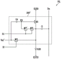
图3A和图3B示出位于第i水平行上并结合到第m数据线Dm的像素PXL的实施例。参照图3A,像素PXL包括有机发光二极管OLED以及用于控制供应到有机发光二极管OLED的电流的量的像素电路2001。有机发光二极管OLED的阳极电极结合到像素电路2001,有机发光二极管OLED的阴极电极结合到第二驱动电源ELVSS。有机发光二极管OLED产生与从像素电路2001供应的电流的量对应的具有预定的亮度的光。3A and 3B illustrate an embodiment of the pixel PXL located on the i-th horizontal row and coupled to the m-th data line Dm. 3A, the pixel PXL includes an organic light emitting diode OLED and a
像素电路2001控制从第一驱动电源ELVDD经由有机发光二极管OLED流动到第二驱动电源ELVSS的电流的量。为此,像素电路2001包括第一晶体管M1至第七晶体管M7、第一稳定化晶体管MS1和存储电容器Cst。The
第一晶体管(或驱动晶体管)M1的第一电极结合到第一节点N1,第一晶体管M1的第二电极经由第七晶体管M7结合到有机发光二极管OLED的阳极电极。另外,第一晶体管M1的栅电极结合到第二节点N2。第一晶体管M1与第二节点N2的电压对应地来控制从第一驱动电源ELVDD经由有机发光二极管OLED流动到第二驱动电源ELVSS的电流的量。为此,第一驱动电源ELVDD被设定为比第二驱动电源ELVSS的电压高的电压。The first electrode of the first transistor (or driving transistor) M1 is coupled to the first node N1, and the second electrode of the first transistor M1 is coupled to the anode electrode of the organic light emitting diode OLED via the seventh transistor M7. In addition, the gate electrode of the first transistor M1 is coupled to the second node N2. The first transistor M1 controls the amount of current flowing from the first driving power source ELVDD to the second driving power source ELVSS via the organic light emitting diode OLED corresponding to the voltage of the second node N2. For this reason, the first driving power supply ELVDD is set to a voltage higher than that of the second driving power supply ELVSS.
第二晶体管M2结合在数据线Dm与第一节点N1之间。此外,第二晶体管M2的栅电极结合到第i第一扫描线S1i。当第一扫描信号供应到第i第一扫描线S1i时,第二晶体管M2导通,以允许数据线Dm和第一节点N1彼此电结合。The second transistor M2 is coupled between the data line Dm and the first node N1. Also, the gate electrode of the second transistor M2 is coupled to the i-th first scan line S1i. When the first scan signal is supplied to the i-th first scan line S1i, the second transistor M2 is turned on to allow the data line Dm and the first node N1 to be electrically coupled to each other.
第三晶体管M3结合在第一晶体管M1的第二电极与第二节点N2之间。另外,第三晶体管M3的栅电极结合到第i第一扫描线S1i并在第一扫描信号供应到第i第一扫描线S1i时导通。The third transistor M3 is coupled between the second electrode of the first transistor M1 and the second node N2. In addition, the gate electrode of the third transistor M3 is coupled to the i-th first scan line S1i and turned on when the first scan signal is supplied to the i-th first scan line S1i.
第一稳定化晶体管MS1结合在第三晶体管M3与第二节点N2之间。另外,第一稳定化晶体管MS1的栅电极结合到控制电源VC。第一稳定化晶体管MS1与控制电源VC的电压对应地导通或截止。第一稳定化晶体管MS1是氧化物半导体晶体管。The first stabilization transistor MS1 is coupled between the third transistor M3 and the second node N2. In addition, the gate electrode of the first stabilization transistor MS1 is coupled to the control power supply VC. The first stabilization transistor MS1 is turned on or off according to the voltage of the control power source VC. The first stabilization transistor MS1 is an oxide semiconductor transistor.
控制电源VC被设定为栅极导通电压,使得当以第一驱动频率(例如,正常驱动频率)驱动像素PXL时第一稳定化晶体管MS1导通。当以第一驱动频率驱动像素PXL时,第一稳定化晶体管MS1保持导通状态。The control power supply VC is set to the gate-on voltage so that the first stabilization transistor MS1 is turned on when the pixel PXL is driven at the first driving frequency (eg, the normal driving frequency). When the pixel PXL is driven at the first driving frequency, the first stabilization transistor MS1 maintains an on state.
在以比第一驱动频率低的第二驱动频率驱动(即,低频率驱动)像素PXL的时间段期间,控制电源VC被设定为栅极截止电压。在以第二驱动频率驱动像素PXL的时间段期间,第一稳定化晶体管MS1保持截止状态。如果第一稳定化晶体管MS1截止,那么来自第二节点N2的漏电流最小化,因此,可在以第二驱动频率驱动像素PXL的时间段期间在像素PXL中实施具有期望的亮度的图像。During a period in which the pixel PXL is driven (ie, driven at a low frequency) at a second driving frequency lower than the first driving frequency, the control power supply VC is set to a gate-off voltage. During the period in which the pixel PXL is driven at the second driving frequency, the first stabilization transistor MS1 maintains an off state. If the first stabilizing transistor MS1 is turned off, the leakage current from the second node N2 is minimized, and thus, an image with desired brightness can be implemented in the pixel PXL during the period in which the pixel PXL is driven at the second driving frequency.
在图3A中,第一稳定化晶体管MS1结合在第三晶体管M3与第二节点N2之间。在一个实施例中,如图3B中所示,第一稳定化晶体管MS1可结合在第一晶体管M1的第二电极与第三晶体管M3之间。In FIG. 3A, the first stabilization transistor MS1 is coupled between the third transistor M3 and the second node N2. In one embodiment, as shown in FIG. 3B, the first stabilization transistor MS1 may be coupled between the second electrode of the first transistor M1 and the third transistor M3.
第四晶体管M4结合在第二节点N2与第一电源Vint之间。第四晶体管M4的栅电极结合到第i第二扫描线S2i。当第二扫描信号供应到第i第二扫描线S2i时,第四晶体管M4导通,以将第一电源Vint的电压供应到第二节点N2。第一电源Vint被设定为比供应到数据线Dm的数据信号低的电压。与供应到第i第一扫描线S1i的第一扫描信号相比,更早地供应供应到第i第二扫描线S2i的第二扫描信号。因此,第i第二扫描线S2i可被设定为第i-1第一扫描线S1i-1。The fourth transistor M4 is coupled between the second node N2 and the first power source Vint. The gate electrode of the fourth transistor M4 is coupled to the i-th second scan line S2i. When the second scan signal is supplied to the i-th second scan line S2i, the fourth transistor M4 is turned on to supply the voltage of the first power source Vint to the second node N2. The first power source Vint is set to a lower voltage than the data signal supplied to the data line Dm. The second scan signal supplied to the i-th second scan line S2i is supplied earlier than the first scan signal supplied to the i-th first scan line S1i. Therefore, the i-th second scan line S2i may be set as the i-1-th first scan line S1i-1.
第五晶体管M5结合在有机发光二极管OLED的阳极电极与第一电源Vint之间。第五晶体管M5的栅电极结合到第i第三扫描线S3i。当第三扫描信号供应到第i第三扫描线S3i时,第五晶体管M5导通,以将第一电源Vint的电压供应到有机发光二极管OLED的阳极电极。供应到第i第三扫描线S3i的第三扫描信号与供应到发光控制线Ei的发光控制信号重叠。因此,第i第三扫描线S3i可被设定为第i第一扫描线S1i或第i第二扫描线S2i。The fifth transistor M5 is coupled between the anode electrode of the organic light emitting diode OLED and the first power source Vint. The gate electrode of the fifth transistor M5 is coupled to the i-th third scan line S3i. When the third scan signal is supplied to the i-th third scan line S3i, the fifth transistor M5 is turned on to supply the voltage of the first power source Vint to the anode electrode of the organic light emitting diode OLED. The third scan signal supplied to the i-th third scan line S3i overlaps with the light emission control signal supplied to the light emission control line Ei. Therefore, the i-th third scan line S3i can be set as the i-th first scan line S1i or the i-th second scan line S2i.
如果第一电源Vint的电压供应到有机发光二极管OLED的阳极电极,那么有机发光二极管OLED的寄生电容器(有机电容器Coled)被放电。如果有机电容器Coled被放电,那么改善像素PXL的黑色表现能力(black expression ability)。If the voltage of the first power source Vint is supplied to the anode electrode of the organic light emitting diode OLED, the parasitic capacitor (organic capacitor Coled) of the organic light emitting diode OLED is discharged. If the organic capacitor Coled is discharged, the black expression ability of the pixel PXL is improved.
例如,在前一帧时间段期间,在有机电容器Coled中充入了与从像素电路2001供应的电流对应的预定的电压。如果有机电容器Coled被充电,那么即使在低电流下有机发光二极管OLED也会容易地发光。For example, during the previous frame period, a predetermined voltage corresponding to the current supplied from the
在当前帧时间段中,可将黑色数据信号(black data signal)供应到像素电路2001。当供应黑色数据信号时,像素电路2001将不向有机发光二极管OLED理想地供应电流。然而,即使供应黑色数据信号时,形成有晶体管的像素电路2001也向有机发光二极管OLED供应预定的漏电流。在此时,如果有机电容器Coled处于充电状态,那么有机发光二极管OLED会微弱地发光。因此,劣化了像素PXL的黑色表现能力。In the current frame period, a black data signal may be supplied to the
另一方面,如果通过第一电源Vint使有机电容器Coled放电,那么有机发光二极管OLED因漏电流被设定为非发光状态。即,在一个实施例中,使用第一电源Vint使有机电容器Coled放电。因此,可改善像素PXL的黑色表现能力。On the other hand, if the organic capacitor Coled is discharged by the first power source Vint, the organic light emitting diode OLED is set to a non-emitting state due to leakage current. That is, in one embodiment, the organic capacitor Coled is discharged using the first power source Vint. Therefore, the black representation capability of the pixel PXL can be improved.
第六晶体管M6结合在第一驱动电源ELVDD与第一节点N1之间。另外,第六晶体管M6的栅电极结合到第i发光控制线Ei。当发光控制信号供应到第i发光控制线Ei时,第六晶体管M6截止,当不供应发光控制信号时,第六晶体管M6导通。The sixth transistor M6 is coupled between the first driving power source ELVDD and the first node N1. In addition, the gate electrode of the sixth transistor M6 is coupled to the i-th light emission control line Ei. The sixth transistor M6 is turned off when the light emission control signal is supplied to the i-th light emission control line Ei, and is turned on when the light emission control signal is not supplied.
第七晶体管M7结合在第一晶体管M1与有机发光二极管OLED的阳极电极之间。另外,第七晶体管M7的栅电极结合到第i发光控制线Ei。当发光控制信号供应到第i发光控制线Ei时,第七晶体管M7截止,当不供应发光控制信号时,第七晶体管M7导通。The seventh transistor M7 is coupled between the first transistor M1 and the anode electrode of the organic light emitting diode OLED. In addition, the gate electrode of the seventh transistor M7 is coupled to the i-th light emission control line Ei. The seventh transistor M7 is turned off when the light emission control signal is supplied to the i-th light emission control line Ei, and is turned on when the light emission control signal is not supplied.
存储电容器Cst结合在第一驱动电源ELVDD与第二节点N2之间。存储电容器Cst充入与数据信号以及第一晶体管M1的阈值电压对应的电压。The storage capacitor Cst is coupled between the first driving power source ELVDD and the second node N2. The storage capacitor Cst is charged with a voltage corresponding to the data signal and the threshold voltage of the first transistor M1.
在本实施例的像素PXL中,第一晶体管M1至第七晶体管M7是P型多晶硅半导体晶体管。具体地,位于用于将电流供应到有机发光二极管OLED的电流供应路径上的晶体管M1、M6和M7是P型多晶硅半导体晶体管。如果晶体管M1至M7是多晶硅半导体晶体管,那么可确保快的驱动特性。In the pixel PXL of the present embodiment, the first to seventh transistors M1 to M7 are P-type polysilicon semiconductor transistors. Specifically, the transistors M1 , M6 and M7 on the current supply path for supplying current to the organic light emitting diode OLED are P-type polysilicon semiconductor transistors. If the transistors M1 to M7 are polycrystalline silicon semiconductor transistors, fast driving characteristics can be ensured.
另外,第一稳定化晶体管MS1是N型氧化物半导体晶体管。如果第一稳定化晶体管MS1是氧化物半导体晶体管,那么可减小来自第二节点N2的漏电流或者使之最小化。因此,可在像素单元100中显示具有期望的亮度的图像。In addition, the first stabilization transistor MS1 is an N-type oxide semiconductor transistor. If the first stabilization transistor MS1 is an oxide semiconductor transistor, the leakage current from the second node N2 can be reduced or minimized. Therefore, an image with desired brightness can be displayed in the
图4示出用于驱动图3A和图3B中的像素PXL的方法的实施例。在图4中,假定将第i第二扫描线S2i设定为第i-1第一扫描线S1i-1,将第i第三扫描线S3i设定为第i第一扫描线S1i。另外,图4的驱动方法对应于第一驱动频率,并假定将第一稳定化晶体管MS1设定为导通状态。Figure 4 illustrates an embodiment of a method for driving the pixel PXL in Figures 3A and 3B. In FIG. 4, it is assumed that the i-th second scan line S2i is set as the i-1th first scan line S1i-1, and the i-th third scan line S3i is set as the i-th first scan line S1i. In addition, the driving method of FIG. 4 corresponds to the first driving frequency, and assumes that the first stabilization transistor MS1 is set to the ON state.
参照图4,在第一时间段T1期间,将发光控制信号供应到第i发光控制线Ei,将第二扫描信号供应到第i第二扫描线S2i。如果将发光控制信号供应到第i发光控制线Ei,那么第六晶体管M6和第七晶体管M7截止。Referring to FIG. 4 , during the first period T1, the light emission control signal is supplied to the i-th light-emitting control line Ei, and the second scan signal is supplied to the i-th second scan line S2i. If the light emission control signal is supplied to the i-th light emission control line Ei, the sixth transistor M6 and the seventh transistor M7 are turned off.
如果第六晶体管M6截止,那么第一驱动电源ELVDD和第一节点N1电中断。如果第七晶体管M7截止,那么第一晶体管M1和有机发光二极管OLED电中断。因此,像素PXL在将发光控制信号供应到第i发光控制线Ei的时间段(即,第一时间段T1和第二时间段T2)期间被设定为非发光状态。If the sixth transistor M6 is turned off, the first driving power supply ELVDD and the first node N1 are electrically interrupted. If the seventh transistor M7 is turned off, the first transistor M1 and the organic light emitting diode OLED are electrically interrupted. Therefore, the pixel PXL is set to a non-emission state during the period (ie, the first period T1 and the second period T2 ) in which the light emission control signal is supplied to the i-th light emission control line Ei.
如果将第二扫描信号供应到第i第二扫描线S2i,那么第四晶体管M4导通。如果第四晶体管M4导通,那么第一电源Vint的电压供应到第二节点N2。If the second scan signal is supplied to the i-th second scan line S2i, the fourth transistor M4 is turned on. If the fourth transistor M4 is turned on, the voltage of the first power source Vint is supplied to the second node N2.
在第二时间段T2期间,将第一扫描信号供应到第i第一扫描线S1i。如果将第一扫描信号供应到第i第一扫描线S1i,那么第二晶体管M2、第三晶体管M3和第五晶体管M5导通。During the second period T2, the first scan signal is supplied to the i-th first scan line S1i. If the first scan signal is supplied to the i-th first scan line S1i, the second transistor M2, the third transistor M3 and the fifth transistor M5 are turned on.
如果第五晶体管M5导通,那么第一电源Vint的电压供应到有机发光二极管OLED的阳极电极。如果第一电源Vint的电压供应到有机发光二极管OLED的阳极电极,那么有机电容器Coled被放电。因此,改善了像素PXL的黑色表现能力。If the fifth transistor M5 is turned on, the voltage of the first power source Vint is supplied to the anode electrode of the organic light emitting diode OLED. If the voltage of the first power source Vint is supplied to the anode electrode of the organic light emitting diode OLED, the organic capacitor Coled is discharged. Therefore, the black performance capability of the pixel PXL is improved.
如果第三晶体管M3导通,那么第一晶体管M1的第二电极和第二节点N2彼此电结合。例如,第一晶体管M1二极管结合。这里,在第二时间段T2期间,将第一稳定化晶体管MS1设定为导通状态。因此,与第三晶体管M3的导通和截止对应地来控制第一晶体管M1的第二电极与第二节点N2之间的电结合。If the third transistor M3 is turned on, the second electrode of the first transistor M1 and the second node N2 are electrically coupled to each other. For example, the first transistor M1 is diode-bonded. Here, during the second period T2, the first stabilization transistor MS1 is set to an on state. Therefore, the electrical coupling between the second electrode of the first transistor M1 and the second node N2 is controlled corresponding to the turn-on and turn-off of the third transistor M3.
如果第二晶体管M2导通,那么来自数据线Dm的数据信号供应到第一节点N1。在此时,由于第二节点N2被初始化为比数据信号低的第一电源Vint的电压,因此第一晶体管M1导通。If the second transistor M2 is turned on, the data signal from the data line Dm is supplied to the first node N1. At this time, since the second node N2 is initialized to the voltage of the first power source Vint lower than the data signal, the first transistor M1 is turned on.
如果第一晶体管M1导通,那么供应到第一节点N1的数据信号经由二极管结合的第一晶体管M1被供应到第二节点N2。在此时,与数据信号和第一晶体管M1的阈值电压对应的电压被施加到第二节点N2。在第二时间段T2期间,存储电容器Cst存储第二节点N2的电压。If the first transistor M1 is turned on, the data signal supplied to the first node N1 is supplied to the second node N2 via the diode-coupled first transistor M1. At this time, a voltage corresponding to the data signal and the threshold voltage of the first transistor M1 is applied to the second node N2. During the second period T2, the storage capacitor Cst stores the voltage of the second node N2.
在第三时间段T3期间,停止向第i发光控制线Ei供应发光控制信号。如果停止向第i发光控制线Ei供应发光控制信号,那么第六晶体管M6和第七晶体管M7导通。During the third time period T3, the supply of the light emission control signal to the i-th light emission control line Ei is stopped. If the supply of the light emission control signal to the i-th light emission control line Ei is stopped, the sixth transistor M6 and the seventh transistor M7 are turned on.
如果第六晶体管M6导通,那么第一驱动电源ELVDD和第一节点N1彼此电结合。如果第七晶体管M7导通,那么第一晶体管M1的第二电极与有机发光二极管OLED的阳极电极彼此电结合。在此时,第一晶体管M1基于施加到第二节点N2的电压控制从第一驱动电源ELVDD经由有机发光二极管OLED流动到第二驱动电源ELVSS的电流的量。If the sixth transistor M6 is turned on, the first driving power source ELVDD and the first node N1 are electrically coupled to each other. If the seventh transistor M7 is turned on, the second electrode of the first transistor M1 and the anode electrode of the organic light emitting diode OLED are electrically coupled to each other. At this time, the first transistor M1 controls the amount of current flowing from the first driving power source ELVDD to the second driving power source ELVSS via the organic light emitting diode OLED based on the voltage applied to the second node N2.
如上所述,在以第一驱动频率驱动像素PXL的时间段期间,像素PXL在重复第一时间段T1至第三时间段T3的同时产生具有预定的亮度的光。另外,在以第一驱动频率驱动像素PXL的时间段期间,第一稳定化晶体管MS1保持导通状态。因此,可稳定地驱动像素PXL。As described above, during the period in which the pixel PXL is driven at the first driving frequency, the pixel PXL generates light having predetermined luminance while repeating the first period T1 to the third period T3. In addition, the first stabilization transistor MS1 maintains an on state during the period in which the pixel PXL is driven at the first driving frequency. Therefore, the pixel PXL can be driven stably.
图5示出在以第二驱动频率驱动图3A和图3B的像素PXL时的实施例。参照图5,低频率驱动意味着在将数据信号供应到像素PXL之后,在将数据信号的电压保持预定时间的同时保持像素PXL的发光的驱动方法。例如,当在像素单元100中显示静态图像时,有机发光显示装置的驱动频率可从第一驱动频率改变成第二驱动频率。如果以第二驱动频率来驱动有机发光显示装置,那么减少供应数据信号的次数。因此,功耗减小。FIG. 5 shows an embodiment when the pixel PXL of FIGS. 3A and 3B is driven at the second driving frequency. 5, the low frequency driving means a driving method of maintaining the light emission of the pixel PXL while maintaining the voltage of the data signal for a predetermined time after the data signal is supplied to the pixel PXL. For example, when a still image is displayed in the
将描述像素PXL的操作过程。在将数据信号供应到像素PXL的第一时间段T1和第二时间段T2期间,将控制电源VC的电压设定为使得第一稳定化晶体管MS1导通。然后,将数据信号的电压正常地供应到各个像素PXL。The operation procedure of the pixel PXL will be described. During the first period T1 and the second period T2 in which the data signal is supplied to the pixel PXL, the voltage of the control power source VC is set so that the first stabilization transistor MS1 is turned on. Then, the voltage of the data signal is normally supplied to each pixel PXL.
在将数据信号供应到各个像素PXL之后,将控制电源VC的电压设定为使得第一稳定化晶体管MS1截止。因此,第一稳定化晶体管MS1截止。After the data signals are supplied to the respective pixels PXL, the voltage of the control power source VC is set so that the first stabilization transistor MS1 is turned off. Therefore, the first stabilization transistor MS1 is turned off.
如果第一稳定化晶体管MS1截止,那么在像素PXL发光的时间段期间可减小来自第二节点N2的漏电流或使之最小化。因此,可从像素PXL产生具有期望的亮度的光。具体地,第一稳定化晶体管MS1形成为具有优异的截止电流特性的氧化物半导体晶体管。因此,可减小来自第二节点N2的漏电流或者使之最小化。If the first stabilizing transistor MS1 is turned off, the leakage current from the second node N2 may be reduced or minimized during the period in which the pixel PXL emits light. Therefore, light with desired luminance can be generated from the pixel PXL. Specifically, the first stabilization transistor MS1 is formed as an oxide semiconductor transistor having excellent off-current characteristics. Therefore, the leakage current from the second node N2 can be reduced or minimized.
图6A和图6B示出根据本公开的另一实施例的包括像素电路2001'和有机发光二极管OLED的像素PXL的额外的实施例。有机发光二极管OLED的阳极电极结合到像素电路2001',有机发光二极管OLED的阴极电极结合到第二驱动电源ELVSS。有机发光二极管OLED产生与从像素电路2001'供应的电流的量对应的具有预定的亮度的光。6A and 6B illustrate additional embodiments of a pixel PXL including a pixel circuit 2001' and an organic light emitting diode OLED according to another embodiment of the present disclosure. The anode electrode of the organic light emitting diode OLED is coupled to the pixel circuit 2001', and the cathode electrode of the organic light emitting diode OLED is coupled to the second driving power source ELVSS. The organic light emitting diode OLED generates light having a predetermined brightness corresponding to the amount of current supplied from the pixel circuit 2001'.
像素电路2001'基于数据信号控制从第一驱动电源ELVDD经由有机发光二极管OLED流动到第二驱动电源ELVSS的电流的量。像素电路2001'包括位于第二节点N2与第一晶体管M1之间的电流路径上的第一稳定化晶体管MS1'。第一稳定化晶体管MS1'可位于第三晶体管M3与第二节点N2之间或者第一晶体管M1的第二电极与第三晶体管M3之间。The pixel circuit 2001' controls the amount of current flowing from the first driving power source ELVDD to the second driving power source ELVSS via the organic light emitting diode OLED based on the data signal. The pixel circuit 2001' includes a first stabilization transistor MS1' on the current path between the second node N2 and the first transistor M1. The first stabilization transistor MS1' may be located between the third transistor M3 and the second node N2 or between the second electrode of the first transistor M1 and the third transistor M3.
第一稳定化晶体管MS1'的栅电极结合到第i发光控制线Ei。当发光控制信号供应到第i发光控制线Ei时,第一稳定化晶体管MS1'导通,当不供应发光控制信号时,第一稳定化晶体管MS1'截止。The gate electrode of the first stabilization transistor MS1' is coupled to the i-th light emission control line Ei. When the light emission control signal is supplied to the i-th light emission control line Ei, the first stabilization transistor MS1' is turned on, and when the light emission control signal is not supplied, the first stabilization transistor MS1' is turned off.
将参照图4、图6A和图6B描述像素PXL的操作过程。在第一时间段T1期间,将发光控制信号供应到第i发光控制线Ei,将第二扫描信号供应到第i第二扫描线S2i。The operation process of the pixel PXL will be described with reference to FIGS. 4 , 6A and 6B. During the first period T1, the light emission control signal is supplied to the i-th light-emitting control line Ei, and the second scan signal is supplied to the i-th second scan line S2i.
如果将发光控制信号供应到第i发光控制线Ei,那么第六晶体管M6和第七晶体管M7截止。因此,像素PXL被设定为非发光状态。如果将第二扫描信号供应到第i第二扫描线S2i,那么第四晶体管M4导通。因此,第二节点N2被初始化为第一电源Vint的电压。另外,如果将发光控制信号供应到第i发光控制线Ei,那么第一稳定化晶体管MS1'导通。If the light emission control signal is supplied to the i-th light emission control line Ei, the sixth transistor M6 and the seventh transistor M7 are turned off. Therefore, the pixel PXL is set to a non-light emitting state. If the second scan signal is supplied to the i-th second scan line S2i, the fourth transistor M4 is turned on. Therefore, the second node N2 is initialized to the voltage of the first power source Vint. In addition, if the light emission control signal is supplied to the i-th light emission control line Ei, the first stabilization transistor MS1' is turned on.
在第二时间段T2期间,将第一扫描信号供应到第i第一扫描线S1i。如果将第一扫描信号供应到第i第一扫描线S1i,那么第二晶体管M2、第三晶体管M3和第五晶体管M5导通。During the second period T2, the first scan signal is supplied to the i-th first scan line S1i. If the first scan signal is supplied to the i-th first scan line S1i, the second transistor M2, the third transistor M3 and the fifth transistor M5 are turned on.
如果第五晶体管M5导通,那么第一电源Vint的电压供应到有机发光二极管OLED的阳极电极。因此,有机电容器Coled被放电。If the fifth transistor M5 is turned on, the voltage of the first power source Vint is supplied to the anode electrode of the organic light emitting diode OLED. Therefore, the organic capacitor Coled is discharged.
如果第三晶体管M3导通,那么第一晶体管M1的第二电极和第二节点N2彼此电结合。即,第一晶体管M1二极管结合。第一稳定化晶体管MS1'在第二时间段T2期间被设定为导通状态。因此,与第三晶体管M3的导通和截止对应地来控制第一晶体管M1的第二电极与第二节点N2之间的电结合。If the third transistor M3 is turned on, the second electrode of the first transistor M1 and the second node N2 are electrically coupled to each other. That is, the first transistor M1 is diode-bonded. The first stabilization transistor MS1 ′ is set to a conducting state during the second period T2 . Therefore, the electrical coupling between the second electrode of the first transistor M1 and the second node N2 is controlled corresponding to the turn-on and turn-off of the third transistor M3.
如果第二晶体管M2导通,那么来自数据线Dm的数据信号被供应到第一节点N1。然后,供应到第一节点N1的数据信号经由二极管连接的第一晶体管M1供应到第二节点N2。在此时,与数据信号和第一晶体管M1的阈值电压对应的电压被施加到第二节点N2。在第二时间段T2期间,第二节点N2的电压存储在存储电容器Cst中。If the second transistor M2 is turned on, the data signal from the data line Dm is supplied to the first node N1. Then, the data signal supplied to the first node N1 is supplied to the second node N2 via the diode-connected first transistor M1. At this time, a voltage corresponding to the data signal and the threshold voltage of the first transistor M1 is applied to the second node N2. During the second period T2, the voltage of the second node N2 is stored in the storage capacitor Cst.
在第三时间段T3期间,停止向第i发光控制线Ei供应发光控制信号。如果停止向第i发光控制线Ei供应发光控制信号,那么第六晶体管M6和第七晶体管M7导通。如果停止向第i发光控制线Ei供应发光控制信号,那么第一稳定化晶体管MS1'截止。During the third time period T3, the supply of the light emission control signal to the i-th light emission control line Ei is stopped. If the supply of the light emission control signal to the i-th light emission control line Ei is stopped, the sixth transistor M6 and the seventh transistor M7 are turned on. If the supply of the light emission control signal to the i-th light emission control line Ei is stopped, the first stabilization transistor MS1 ′ is turned off.
如果第六晶体管M6和第七晶体管M7导通,那么形成电流从第一驱动电源ELVDD经由第六晶体管M6、第一晶体管M1、第七晶体管M7和有机发光二极管OLED流动到第二驱动电源ELVSS所沿的电流路径。在此时,第一晶体管M1与施加到第二节点N2的电压对应地来控制从第一驱动电源ELVDD经由有机发光二极管OLED流动到第二驱动电源ELVSS的电流的量。If the sixth transistor M6 and the seventh transistor M7 are turned on, a current is formed to flow from the first driving power source ELVDD to the second driving power source ELVSS via the sixth transistor M6, the first transistor M1, the seventh transistor M7 and the organic light emitting diode OLED. along the current path. At this time, the first transistor M1 controls the amount of current flowing from the first driving power source ELVDD to the second driving power source ELVSS via the organic light emitting diode OLED corresponding to the voltage applied to the second node N2.
同时,在像素PXL发光的第三时间段T3期间,第一稳定化晶体管MS1'保持截止状态。如果第一稳定化晶体管MS1'截止,那么在像素PXL发光的时间段期间可减小来自第二节点N2的漏电流或使之最小化,因此,可从像素PXL产生具有期望的亮度的光。Meanwhile, during the third period T3 in which the pixel PXL emits light, the first stabilization transistor MS1 ′ maintains an off state. If the first stabilizing transistor MS1 ′ is turned off, leakage current from the second node N2 may be reduced or minimized during a period in which the pixel PXL emits light, and thus, light with desired luminance may be generated from the pixel PXL.
图7A和图7B示出包括像素电路2002和有机发光二极管OLED的像素PXL的额外的实施例。有机发光二极管OLED的阳极电极结合到像素电路2002,有机发光二极管OLED的阴极电极结合到第二驱动电源ELVSS。有机发光二极管OLED产生与从像素电路2002供应的电流的量对应的具有预定的亮度的光。7A and 7B illustrate additional embodiments of a pixel PXL including a
像素电路2002与数据信号对应地来控制从第一驱动电源ELVDD经由有机发光二极管OLED流动到第二驱动电源ELVSS的电流的量。The
像素电路2002包括位于第二节点N2与第一电源Vint之间的电流路径上的第二稳定化晶体管MS2。例如,第二稳定化晶体管MS2可位于第二节点N2与第四晶体管M4之间或者第四晶体管M4与第一电源Vint之间。The
第二稳定化晶体管MS2的栅电极结合到控制电源VC。当以第一驱动频率驱动有机发光显示装置时,第二稳定化晶体管MS2保持导通状态。像素PXL的操作过程可与参照图3A至图4描述的操作过程相同。The gate electrode of the second stabilization transistor MS2 is coupled to the control power supply VC. When the organic light emitting display device is driven at the first driving frequency, the second stabilization transistor MS2 maintains an on state. The operation process of the pixel PXL may be the same as that described with reference to FIGS. 3A to 4 .
同时,在以第二驱动频率驱动有机发光显示装置的时间段(即,以低频率驱动有机发光显示装置的时间段)期间,第二稳定化晶体管MS2截止。在此时,在如图5中示出的将数据信号供应到像素PXL的第一时间段T1和第二时间段T2期间,将控制电源VC的电压设定为使得第二稳定化晶体管MS2导通。然后,将数据信号的电压正常地供应到各个像素PXL。Meanwhile, during a period in which the organic light emitting display device is driven at the second driving frequency (ie, a period in which the organic light emitting display device is driven at a low frequency), the second stabilization transistor MS2 is turned off. At this time, during the first period T1 and the second period T2 in which the data signal is supplied to the pixel PXL as shown in FIG. 5 , the voltage of the control power source VC is set such that the second stabilization transistor MS2 conducts Pass. Then, the voltage of the data signal is normally supplied to each pixel PXL.
在将数据信号供应到各个像素PXL之后,将控制电源VC的电压设定为使得第二稳定化晶体管MS2截止。因此,第二稳定化晶体管MS2截止。After the data signals are supplied to the respective pixels PXL, the voltage of the control power supply VC is set so that the second stabilization transistor MS2 is turned off. Therefore, the second stabilization transistor MS2 is turned off.
如果第二稳定化晶体管MS2截止,那么减小了第二节点N2与第一电源Vint之间的漏电流或使之最小化。因此,可显示具有期望的亮度的图像。在本公开的实施例中,第二稳定化晶体管MS2形成为氧化物半导体晶体管。因此,可减小漏电流或者使之最小化。If the second stabilization transistor MS2 is turned off, the leakage current between the second node N2 and the first power source Vint is reduced or minimized. Therefore, an image with desired brightness can be displayed. In an embodiment of the present disclosure, the second stabilization transistor MS2 is formed as an oxide semiconductor transistor. Therefore, leakage current can be reduced or minimized.
同时,在图7A和图7B中,与图3A、图3B、图6A和图6B相比,已经示出去除了第一稳定化晶体管MS1或MS1',但是本公开不限于此。例如,第一稳定化晶体管MS1或MS1'可被添加到图7A和图7B的像素PXL。Meanwhile, in FIGS. 7A and 7B , compared with FIGS. 3A , 3B, 6A and 6B, it has been shown that the first stabilization transistor MS1 or MS1 ′ is removed, but the present disclosure is not limited thereto. For example, a first stabilization transistor MS1 or MS1 ′ may be added to the pixel PXL of FIGS. 7A and 7B .
图8A和图8B示出包括像素电路2002'和有机发光二极管OLED的像素PXL的额外的实施例。有机发光二极管OLED的阳极电极结合到像素电路2002',有机发光二极管OLED的阴极电极结合到第二驱动电源ELVSS。有机发光二极管OLED产生与从像素电路2002'供应的电流的量对应的具有预定的亮度的光。8A and 8B illustrate additional embodiments of a pixel PXL including a pixel circuit 2002' and an organic light emitting diode OLED. The anode electrode of the organic light emitting diode OLED is coupled to the pixel circuit 2002', and the cathode electrode of the organic light emitting diode OLED is coupled to the second driving power source ELVSS. The organic light emitting diode OLED generates light having a predetermined brightness corresponding to the amount of current supplied from the pixel circuit 2002'.
像素电路2002'与数据信号对应地来控制从第一驱动电源ELVDD经由有机发光二极管OLED流动到第二驱动电源ELVSS的电流的量。The pixel circuit 2002' controls the amount of current flowing from the first driving power source ELVDD to the second driving power source ELVSS via the organic light emitting diode OLED, corresponding to the data signal.
像素电路2002'包括位于第二节点N2与第一电源Vint之间的电流路径上的第二稳定化晶体管MS2'。例如,第二稳定化晶体管MS2'可位于第二节点N2与第四晶体管M4之间或者第四晶体管M4与第一电源Vint之间。The pixel circuit 2002' includes a second stabilizing transistor MS2' on the current path between the second node N2 and the first power supply Vint. For example, the second stabilizing transistor MS2' may be located between the second node N2 and the fourth transistor M4 or between the fourth transistor M4 and the first power source Vint.
第二稳定化晶体管MS2'的栅电极结合到第i发光控制线Ei。当发光控制信号供应到第i发光控制线Ei时,第二稳定化晶体管MS2'导通,当不供应发光控制信号时,第二稳定化晶体管MS2'截止。像素PXL的操作过程可与参照图4、图6A和图6B描述的操作过程相同。The gate electrode of the second stabilization transistor MS2' is coupled to the i-th light emission control line Ei. When the light emission control signal is supplied to the i-th light emission control line Ei, the second stabilization transistor MS2' is turned on, and when the light emission control signal is not supplied, the second stabilization transistor MS2' is turned off. The operation process of the pixel PXL may be the same as that described with reference to FIGS. 4 , 6A, and 6B.
如果第二稳定化晶体管MS2'截止,那么减小了第二节点N2与第一电源Vint之间的漏电流或使之最小化。因此,可显示具有期望的亮度的图像。在本实施例中,第二稳定化晶体管MS2'是氧化物半导体晶体管,因此,可使漏电流最小化。If the second stabilization transistor MS2' is turned off, the leakage current between the second node N2 and the first power source Vint is reduced or minimized. Therefore, an image with desired brightness can be displayed. In this embodiment, the second stabilizing transistor MS2' is an oxide semiconductor transistor, and therefore, leakage current can be minimized.
同时,在图8A和图8B中,与图3A、图3B、图6A和图6B相比,已经示出去除了第一稳定化晶体管MS1或MS1',但是本公开不限于此。例如,第一稳定化晶体管MS1或MS1'可添加到图8A和图8B的像素PXL。Meanwhile, in FIGS. 8A and 8B , compared with FIGS. 3A , 3B, 6A and 6B, it has been shown that the first stabilization transistor MS1 or MS1 ′ is removed, but the present disclosure is not limited thereto. For example, a first stabilization transistor MS1 or MS1 ′ may be added to the pixel PXL of FIGS. 8A and 8B .
图9A和图9B示出包括像素电路2003和有机发光二极管OLED的像素PXL的额外的实施例。有机发光二极管OLED的阳极电极连接到像素电路2003,有机发光二极管OLED的阴极电极连接到第二驱动电源ELVSS。有机发光二极管OLED产生与从像素电路2003供应的电流的量对应的具有预定的亮度的光。9A and 9B illustrate additional embodiments of a pixel PXL including a
像素电路2003与数据信号对应地来控制从第一驱动电源ELVDD经由有机发光二极管OLED流动到第二驱动电源ELVSS的电流的量。The
像素电路2003包括位于有机发光二极管OLED的阳极电极与第一电源Vint之间的电流路径上的第三稳定化晶体管MS3。例如,第三稳定化晶体管MS3可位于有机发光二极管OLED的阳极电极与第五晶体管M5之间或者第五晶体管M5与第一电源Vint之间。The
第三稳定化晶体管MS3的栅电极结合到控制电源VC。当以第一驱动频率驱动有机发光显示装置时,第三稳定化晶体管MS3保持导通状态。像素PXL的操作过程可与参照图3A至图4描述的操作过程相同。The gate electrode of the third stabilization transistor MS3 is coupled to the control power supply VC. When the organic light emitting display device is driven at the first driving frequency, the third stabilization transistor MS3 maintains an on state. The operation process of the pixel PXL may be the same as that described with reference to FIGS. 3A to 4 .
同时,在以第二驱动频率驱动有机发光显示装置的时间段(即,以低频率驱动有机发光显示装置的时间段)期间,第三稳定化晶体管MS3截止。在此时,在将数据信号供应到像素PXL的第一时间段T1和第二时间段T2期间,将控制电源VC的电压设定为使得第三稳定化晶体管MS3导通。然后,将数据信号的电压正常地供应到各个像素PXL。Meanwhile, during a period in which the organic light emitting display device is driven at the second driving frequency (ie, a period in which the organic light emitting display device is driven at a low frequency), the third stabilization transistor MS3 is turned off. At this time, during the first period T1 and the second period T2 in which the data signal is supplied to the pixel PXL, the voltage of the control power source VC is set so that the third stabilization transistor MS3 is turned on. Then, the voltage of the data signal is normally supplied to each pixel PXL.
在将数据信号供应到各个像素PXL之后,将控制电源VC的电压设定为使得第三稳定化晶体管MS3截止。因此,第三稳定化晶体管MS3截止。After the data signals are supplied to the respective pixels PXL, the voltage of the control power supply VC is set so that the third stabilization transistor MS3 is turned off. Therefore, the third stabilization transistor MS3 is turned off.
如果第三稳定化晶体管MS3截止,那么减小了有机发光二极管OLED的阳极电极与第一电源Vint之间的漏电流或使之最小化。因此,可显示具有期望的亮度的图像。在本实施例中,第三稳定化晶体管MS3是氧化物半导体晶体管。因此,可减小漏电流或者使之最小化。If the third stabilization transistor MS3 is turned off, the leakage current between the anode electrode of the organic light emitting diode OLED and the first power source Vint is reduced or minimized. Therefore, an image with desired brightness can be displayed. In this embodiment, the third stabilization transistor MS3 is an oxide semiconductor transistor. Therefore, leakage current can be reduced or minimized.
在图9A和图9B中,与图3A、图3B、图6A和图6B相比,已经示出去除了第一稳定化晶体管MS1或MS1',但是本公开不限于此。例如,第一稳定化晶体管MS1或MS1'可被添加到图9A和图9B的像素PXL。In FIGS. 9A and 9B , compared with FIGS. 3A , 3B, 6A and 6B, it has been shown that the first stabilization transistor MS1 or MS1 ′ is removed, but the present disclosure is not limited thereto. For example, a first stabilization transistor MS1 or MS1 ′ may be added to the pixel PXL of FIGS. 9A and 9B .
图10A和图10B示出包括像素电路2003'和有机发光二极管OLED的像素PXL的额外的实施例。有机发光二极管OLED的阳极电极结合到像素电路2003',有机发光二极管OLED的阴极电极结合到第二驱动电源ELVSS。有机发光二极管OLED产生与从像素电路2003'供应的电流的量对应的具有预定的亮度的光。Figures 10A and 10B illustrate additional embodiments of a pixel PXL comprising a pixel circuit 2003' and an organic light emitting diode OLED. The anode electrode of the organic light emitting diode OLED is coupled to the pixel circuit 2003', and the cathode electrode of the organic light emitting diode OLED is coupled to the second driving power source ELVSS. The organic light emitting diode OLED generates light having a predetermined luminance corresponding to the amount of current supplied from the pixel circuit 2003'.
像素电路2003'包括位于有机发光二极管OLED的阳极电极与第一电源Vint之间的电流路径上的第三稳定化晶体管MS3'。例如,第三稳定化晶体管MS3'可位于有机发光二极管OLED的阳极电极与第五晶体管M5之间或者第五晶体管M5与第一电源Vint之间。The pixel circuit 2003' includes a third stabilizing transistor MS3' on the current path between the anode electrode of the organic light emitting diode OLED and the first power source Vint. For example, the third stabilization transistor MS3' may be located between the anode electrode of the organic light emitting diode OLED and the fifth transistor M5 or between the fifth transistor M5 and the first power source Vint.
第三稳定化晶体管MS3'的栅电极结合到第i发光控制线Ei。当发光控制信号供应到第i发光控制线Ei时,第三稳定化晶体管MS3'导通,当不供应发光控制信号时,第三稳定化晶体管MS3'截止。像素PXL的操作过程与参照图4、图6A和图6B描述的操作过程相同。The gate electrode of the third stabilization transistor MS3' is coupled to the i-th light emission control line Ei. When the light emission control signal is supplied to the i-th light emission control line Ei, the third stabilization transistor MS3' is turned on, and when the light emission control signal is not supplied, the third stabilization transistor MS3' is turned off. The operation process of the pixel PXL is the same as that described with reference to FIGS. 4 , 6A and 6B.
如果第三稳定化晶体管MS3'截止,那么减小了有机发光二极管OLED的阳极电极与第一电源Vint之间的漏电流或使之最小化。因此,可显示具有期望的亮度的图像。在本实施例中,第三稳定化晶体管MS3'是氧化物半导体晶体管。因此,可减小漏电流或者使之最小化。If the third stabilization transistor MS3' is turned off, the leakage current between the anode electrode of the organic light emitting diode OLED and the first power source Vint is reduced or minimized. Therefore, an image with desired brightness can be displayed. In this embodiment, the third stabilization transistor MS3' is an oxide semiconductor transistor. Therefore, leakage current can be reduced or minimized.
同时,在图10A和图10B中,与图3A、图3B、图6A和图6B相比,已经示出去除了第一稳定化晶体管MS1或MS1',但是本公开不限于此。例如,第一稳定化晶体管MS1或MS1'可被添加到图10A和图10B的像素PXL。Meanwhile, in FIGS. 10A and 10B , compared with FIGS. 3A , 3B, 6A and 6B, it has been shown that the first stabilization transistor MS1 or MS1 ′ is removed, but the present disclosure is not limited thereto. For example, a first stabilization transistor MS1 or MS1 ′ may be added to the pixel PXL of FIGS. 10A and 10B .
在本实施例中,第一稳定化晶体管MS1或MS1'、第二稳定化晶体管MS2或MS2'以及第三稳定化晶体管MS3或MS3'中的至少一个晶体管可形成在像素PXL中。例如,如图11A至图11D中示出的,第一稳定化晶体管MS1或MS1'、第二稳定化晶体管MS2或MS2'以及第三稳定化晶体管MS3或MS3'可形成在像素PXL中。In the present embodiment, at least one of the first stabilization transistor MS1 or MS1 ′, the second stabilization transistor MS2 or MS2 ′, and the third stabilization transistor MS3 or MS3 ′ may be formed in the pixel PXL. For example, as shown in FIGS. 11A to 11D , a first stabilization transistor MS1 or MS1 ′, a second stabilization transistor MS2 or MS2 ′, and a third stabilization transistor MS3 or MS3 ′ may be formed in the pixel PXL.
如果第一稳定化晶体管MS1或MS1'、第二稳定化晶体管MS2或MS2'以及第三稳定化晶体管MS3或MS3'形成在像素PXL中,那么在有机发光二极管OLED发光的第三时间段T3期间,减小了漏电流或使之最小化。因此,可显示具有期望的亮度的图像。具体地,第一稳定化晶体管MS1或MS1'、第二稳定化晶体管MS2或MS2'以及第三稳定化晶体管MS3或MS3'形成为氧化物半导体晶体管,即使当以低频率驱动像素PXL时,也可稳定地显示具有期望的亮度的图像。If the first stabilization transistor MS1 or MS1 ′, the second stabilization transistor MS2 or MS2 ′, and the third stabilization transistor MS3 or MS3 ′ are formed in the pixel PXL, during the third period T3 in which the organic light emitting diode OLED emits light , reducing or minimizing leakage current. Therefore, an image with desired brightness can be displayed. Specifically, the first stabilization transistor MS1 or MS1 ′, the second stabilization transistor MS2 or MS2 ′, and the third stabilization transistor MS3 or MS3 ′ are formed as oxide semiconductor transistors, even when the pixel PXL is driven at a low frequency Images with desired brightness can be displayed stably.
图12A和图12B示出包括有机发光二极管OLED以及用于控制供应到有机发光二极管OLED的电流的量的像素电路2004的像素PXL的额外的实施例。有机发光二极管OLED的阳极电极结合到像素电路2004,有机发光二极管OLED的阴极电极结合到第二驱动电源ELVSS。有机发光二极管OLED产生与从像素电路2004供应的电流的量对应的具有预定的亮度的光。12A and 12B illustrate additional embodiments of a pixel PXL including an organic light emitting diode OLED and a
像素电路2004与数据信号对应地来控制从第一驱动电源ELVDD经由有机发光二极管OLED流动到第二驱动电源ELVSS的电流的量。为此,像素电路2004包括第十一晶体管M11至第十三晶体管M13、第四稳定化晶体管MS4和存储电容器Cst。The
第十一晶体管(或驱动晶体管)M11的第一电极经由第十三晶体管M13结合到第一驱动电源ELVDD,第十一晶体管M11的第二电极结合到有机发光二极管OLED的阳极电极。另外,第十一晶体管M11的栅电极结合到第十一节点N11。第十一晶体管M11与第十一节点N11的电压对应地来控制从第一驱动电源ELVDD经由有机发光二极管OLED流动到第二驱动电源ELVSS的电流的量。The first electrode of the eleventh transistor (or driving transistor) M11 is coupled to the first driving power source ELVDD via the thirteenth transistor M13, and the second electrode of the eleventh transistor M11 is coupled to the anode electrode of the organic light emitting diode OLED. In addition, the gate electrode of the eleventh transistor M11 is coupled to the eleventh node N11. The eleventh transistor M11 controls the amount of current flowing from the first driving power source ELVDD to the second driving power source ELVSS via the organic light emitting diode OLED corresponding to the voltage of the eleventh node N11.
第十二晶体管M12结合在数据线D与第十一节点N11之间。另外,第十二晶体管M12的栅电极结合到扫描线S。当扫描信号供应到扫描线S时,第十二晶体管M12导通。The twelfth transistor M12 is coupled between the data line D and the eleventh node N11. In addition, the gate electrode of the twelfth transistor M12 is coupled to the scan line S. When the scan signal is supplied to the scan line S, the twelfth transistor M12 is turned on.
第十三晶体管M13结合在第一驱动电源ELVDD与第十一晶体管M11的第一电极之间。另外,第十三晶体管M13的栅电极结合到发光控制线E。当发光控制信号供应到发光控制线E时,第十三晶体管M13截止,当不供应发光控制信号时,第十三晶体管M13导通。The thirteenth transistor M13 is coupled between the first driving power source ELVDD and the first electrode of the eleventh transistor M11. In addition, the gate electrode of the thirteenth transistor M13 is coupled to the light emission control line E. When the light emission control signal is supplied to the light emission control line E, the thirteenth transistor M13 is turned off, and when the light emission control signal is not supplied, the thirteenth transistor M13 is turned on.
第四稳定化晶体管MS4位于数据线D与第十一节点N11之间的电流路径上。例如,第四稳定化晶体管MS4可位于第十二晶体管M12与第十一节点N11之间或者数据线D与第十二晶体管M12之间。The fourth stabilization transistor MS4 is located on the current path between the data line D and the eleventh node N11. For example, the fourth stabilization transistor MS4 may be located between the twelfth transistor M12 and the eleventh node N11 or between the data line D and the twelfth transistor M12.
第四稳定化晶体管MS4的栅电极结合到控制电源VC。当以第一驱动频率驱动有机发光显示装置时,第四稳定化晶体管MS4保持导通状态。另外,第四稳定化晶体管MS4在以第二驱动频率驱动有机发光显示装置之后截止,并且与数据信号对应的电压充入存储电容器Cst中。The gate electrode of the fourth stabilization transistor MS4 is coupled to the control power supply VC. When the organic light emitting display device is driven at the first driving frequency, the fourth stabilization transistor MS4 maintains an on state. In addition, the fourth stabilization transistor MS4 is turned off after driving the organic light emitting display device at the second driving frequency, and a voltage corresponding to the data signal is charged into the storage capacitor Cst.
同时,第四稳定化晶体管MS4是氧化物半导体晶体管。因此,如果第四稳定化晶体管MS4截止,那么减小了数据线D与第十一节点N11之间的漏电流或使之最小化。因此,可在像素PXL中实施具有期望的亮度的图像。Meanwhile, the fourth stabilization transistor MS4 is an oxide semiconductor transistor. Therefore, if the fourth stabilization transistor MS4 is turned off, the leakage current between the data line D and the eleventh node N11 is reduced or minimized. Therefore, an image with a desired brightness can be implemented in the pixel PXL.
存储电容器Cst结合在第十一节点N11与有机发光二极管OLED的阳极电极之间。存储电容器Cst存储与数据信号对应的电压。The storage capacitor Cst is coupled between the eleventh node N11 and the anode electrode of the organic light emitting diode OLED. The storage capacitor Cst stores a voltage corresponding to the data signal.
同时,在根据本实施例的上述像素PXL中,第十一晶体管M11至第十三晶体管M13是N型多晶硅半导体晶体管。如上所述,如果晶体管M11至M13形成为多晶硅半导体晶体管,那么可确保快的驱动特性。Meanwhile, in the above-described pixel PXL according to the present embodiment, the eleventh transistor M11 to the thirteenth transistor M13 are N-type polysilicon semiconductor transistors. As described above, if the transistors M11 to M13 are formed as polycrystalline silicon semiconductor transistors, fast driving characteristics can be ensured.
图13示出用于驱动像素(例如可以是图12A和图12B中示出的像素PXL)的方法的另一实施例。参照图13,首先,将发光控制信号供应到发光控制线E,使得第十三晶体管M13截止。如果第十三晶体管M13截止,那么第一驱动电源ELVDD和第十一晶体管M11电中断,因此,像素PXL被设定为非发光状态。Figure 13 illustrates another embodiment of a method for driving a pixel, which may be, for example, the pixel PXL shown in Figures 12A and 12B. Referring to FIG. 13 , first, a light emission control signal is supplied to the light emission control line E, so that the thirteenth transistor M13 is turned off. If the thirteenth transistor M13 is turned off, the first driving power source ELVDD and the eleventh transistor M11 are electrically interrupted, and thus, the pixel PXL is set to a non-light emitting state.
在那之后,将扫描信号供应到扫描线S,使得第十二晶体管M12导通。如果第十二晶体管M12导通,那么数据线D和第十一节点N11彼此电结合。然后,将来自数据线D的数据信号供应到第十一节点N11。因此,与数据信号对应的电压存储在存储电容器Cst中。After that, the scan signal is supplied to the scan line S, so that the twelfth transistor M12 is turned on. If the twelfth transistor M12 is turned on, the data line D and the eleventh node N11 are electrically coupled to each other. Then, the data signal from the data line D is supplied to the eleventh node N11. Therefore, the voltage corresponding to the data signal is stored in the storage capacitor Cst.
在与数据信号对应的电压存储在存储电容器Cst中之后,停止向发光控制线E供应发光控制信号。如果停止向发光控制线E供应发光控制信号,那么第十三晶体管M13导通。如果第十三晶体管M13导通,那么第一驱动电源ELVDD和第十一晶体管M11彼此电结合。After the voltage corresponding to the data signal is stored in the storage capacitor Cst, the supply of the light emission control signal to the light emission control line E is stopped. If the supply of the light emission control signal to the light emission control line E is stopped, the thirteenth transistor M13 is turned on. If the thirteenth transistor M13 is turned on, the first driving power source ELVDD and the eleventh transistor M11 are electrically coupled to each other.
在此时,第十一晶体管M11基于第十一节点N11的电压控制从第一驱动电源ELVDD经由有机发光二极管OLED流动到第二驱动电源ELVSS的电流的量。At this time, the eleventh transistor M11 controls the amount of current flowing from the first driving power source ELVDD to the second driving power source ELVSS via the organic light emitting diode OLED based on the voltage of the eleventh node N11.
如上所述,在以第一驱动频率驱动有机发光显示装置的时间段期间,本实施例的像素PXL在重复上述过程的同时产生具有预定的亮度的光。另外,在以第一驱动频率驱动有机发光显示装置的时间段期间,第四稳定化晶体管MS4保持导通状态。因此,可稳定地驱动像素PXL。As described above, during the period in which the organic light emitting display device is driven at the first driving frequency, the pixel PXL of the present embodiment generates light having a predetermined luminance while repeating the above-described process. In addition, the fourth stabilization transistor MS4 maintains an on state during the period in which the organic light emitting display device is driven at the first driving frequency. Therefore, the pixel PXL can be driven stably.
此外,在以第二驱动频率驱动有机发光显示装置的期间,与数据信号对应的电压充入各个像素PXL的存储电容器Cst中,将控制电源VC设定为栅极截止电压。然后,各个像素PXL中的第四稳定化晶体管MS4截止。因此,可减小数据线D与第十一节点N11之间的漏电流或使之最小化。因此,即使当以第二驱动频率驱动有机发光显示装置时,像素PXL也可稳定地产生具有期望的亮度的光。In addition, during the period in which the organic light emitting display device is driven at the second driving frequency, the voltage corresponding to the data signal is charged into the storage capacitor Cst of each pixel PXL, and the control power source VC is set to the gate-off voltage. Then, the fourth stabilization transistor MS4 in each pixel PXL is turned off. Therefore, the leakage current between the data line D and the eleventh node N11 can be reduced or minimized. Therefore, even when the organic light emitting display device is driven at the second driving frequency, the pixels PXL can stably generate light with desired luminance.
同时,在本实施例中,图12A和图12B的像素PXL的驱动方法不限于图13的驱动方法。例如,可使用当前已被本领域知晓的各种类型的驱动波形来驱动图12A和图12B的像素PXL。Meanwhile, in the present embodiment, the driving method of the pixel PXL of FIGS. 12A and 12B is not limited to the driving method of FIG. 13 . For example, the pixels PXL of FIGS. 12A and 12B may be driven using various types of drive waveforms currently known in the art.
图14A和图14B示出包括像素电路2004'和有机发光二极管OLED的像素PXL的额外的实施例。有机发光二极管OLED的阳极电极结合到像素电路2004',有机发光二极管OLED的阴极电极结合到第二驱动电源ELVSS。有机发光二极管OLED产生与从像素电路2004'供应的电流对应的具有预定的亮度的光。14A and 14B illustrate additional embodiments of a pixel PXL including a pixel circuit 2004' and an organic light emitting diode OLED. The anode electrode of the organic light emitting diode OLED is coupled to the pixel circuit 2004', and the cathode electrode of the organic light emitting diode OLED is coupled to the second driving power source ELVSS. The organic light emitting diode OLED generates light having a predetermined brightness corresponding to the current supplied from the pixel circuit 2004'.
像素电路2004'基于数据信号控制从第一驱动电源ELVDD经由有机发光二极管OLED流动到第二驱动电源ELVSS的电流的量。The pixel circuit 2004' controls the amount of current flowing from the first driving power source ELVDD to the second driving power source ELVSS via the organic light emitting diode OLED based on the data signal.
像素电路2004'包括位于数据线D与第十一节点N11之间的电流路径上的第四稳定化晶体管MS4'。例如,第四稳定化晶体管MS4'可位于第十二晶体管M12与第十一节点N11之间或者数据线D与第十二晶体管M12之间。The pixel circuit 2004' includes a fourth stabilizing transistor MS4' on the current path between the data line D and the eleventh node N11. For example, the fourth stabilization transistor MS4' may be located between the twelfth transistor M12 and the eleventh node N11 or between the data line D and the twelfth transistor M12.
第四稳定化晶体管MS4'的栅电极结合到扫描线S。当扫描信号供应到扫描线S时,第四稳定化晶体管MS4'导通,当不供应扫描信号时,第四稳定化晶体管MS4'截止。即,第四稳定化晶体管MS4'与第十二晶体管M12同时地导通或截止。The gate electrode of the fourth stabilization transistor MS4' is coupled to the scan line S. When the scan signal is supplied to the scan line S, the fourth stabilization transistor MS4' is turned on, and when the scan signal is not supplied, the fourth stabilization transistor MS4' is turned off. That is, the fourth stabilization transistor MS4' is turned on or off simultaneously with the twelfth transistor M12.
将参照图13、图14A和图14B描述像素PXL的操作过程。首先,将发光控制信号供应到发光控制线E,使得第十三晶体管M13截止。如果第十三晶体管M13截止,那么像素PXL被设定为非发光状态。The operation process of the pixel PXL will be described with reference to FIGS. 13 , 14A, and 14B. First, the light emission control signal is supplied to the light emission control line E, so that the thirteenth transistor M13 is turned off. If the thirteenth transistor M13 is turned off, the pixel PXL is set to a non-emission state.
在那之后,将扫描信号供应到扫描线S,使得第十二晶体管M12和第四稳定化晶体管MS4'导通。如果第十二晶体管M12和第四稳定化晶体管MS4'导通,那么数据线D和第十一节点N11彼此电结合。然后,将来自数据线D的数据信号供应到第十一节点N11。因此,与数据信号对应的电压存储在存储电容器Cst中。After that, the scan signal is supplied to the scan line S, so that the twelfth transistor M12 and the fourth stabilization transistor MS4' are turned on. If the twelfth transistor M12 and the fourth stabilization transistor MS4' are turned on, the data line D and the eleventh node N11 are electrically coupled to each other. Then, the data signal from the data line D is supplied to the eleventh node N11. Therefore, the voltage corresponding to the data signal is stored in the storage capacitor Cst.
在与数据信号对应的电压存储在存储电容器Cst中之后,停止向发光控制线E供应发光控制信号。如果停止向发光控制线E供应发光控制信号,那么第十三晶体管M13导通。如果第十三晶体管M13导通,那么第一驱动电源ELVDD和第十一晶体管M11彼此电结合。After the voltage corresponding to the data signal is stored in the storage capacitor Cst, the supply of the light emission control signal to the light emission control line E is stopped. If the supply of the light emission control signal to the light emission control line E is stopped, the thirteenth transistor M13 is turned on. If the thirteenth transistor M13 is turned on, the first driving power source ELVDD and the eleventh transistor M11 are electrically coupled to each other.
在此时,第十一晶体管M11与第十一节点N11的电压对应地来控制从第一驱动电源ELVDD经由有机发光二极管OLED流动到第二驱动电源ELVSS的电流的量。At this time, the eleventh transistor M11 controls the amount of current flowing from the first driving power source ELVDD to the second driving power source ELVSS via the organic light emitting diode OLED corresponding to the voltage of the eleventh node N11.
同时,第四稳定化晶体管MS4'在像素PXL发光的时间段期间保持截止状态。如果第四稳定化晶体管MS4'截止,那么在像素PXL发光的时间段期间,可减小数据线D与第十一节点N11之间的漏电流或使之最小化。因此,可从像素PXL产生具有期望的亮度的光。Meanwhile, the fourth stabilization transistor MS4' maintains an off state during the period in which the pixel PXL emits light. If the fourth stabilizing transistor MS4' is turned off, the leakage current between the data line D and the eleventh node N11 may be reduced or minimized during a period in which the pixel PXL emits light. Therefore, light with desired luminance can be generated from the pixel PXL.
图15A和图15B示出位于第i水平行上并结合到第m数据线Dm的像素PXL的额外的实施例。参照图15A和图15B,像素PXL包括有机发光二极管OLED以及用于控制供应到有机发光二极管OLED的电流的量的像素电路2005。有机发光二极管OLED的阳极电极结合到像素电路2005,有机发光二极管OLED的阴极电极结合到第二驱动电源ELVSS。有机发光二极管OLED产生与从像素电路2005供应的电流的量对应的具有预定的亮度的光。15A and 15B illustrate additional embodiments of the pixel PXL located on the i-th horizontal row and coupled to the m-th data line Dm. 15A and 15B, the pixel PXL includes an organic light emitting diode OLED and a
像素电路2005与数据信号对应地来控制从第一驱动电源ELVDD经由有机发光二极管OLED流动到第二驱动电源ELVSS的电流的量。为此,像素电路2005包括第二十一晶体管M21至第二十六晶体管M26、第五稳定化晶体管MS5和存储电容器Cst。The
第二十一晶体管(驱动晶体管)M21的第一电极经由第二十六晶体管M26结合到第一驱动电源ELVDD,第二十一晶体管M21的第二电极结合到有机发光二极管OLED的阳极电极。另外,第二十一晶体管M21的栅电极结合到第二十一节点N21。第二十一晶体管M21与第二十一节点N21的电压对应地来控制从第一驱动电源ELVDD经由有机发光二极管OLED流动到第二驱动电源ELVSS的电流的量。The first electrode of the twenty-first transistor (driving transistor) M21 is coupled to the first driving power source ELVDD via the twenty-sixth transistor M26, and the second electrode of the twenty-first transistor M21 is coupled to the anode electrode of the organic light emitting diode OLED. In addition, the gate electrode of the twenty-first transistor M21 is coupled to the twenty-first node N21. The twenty-first transistor M21 controls the amount of current flowing from the first driving power source ELVDD to the second driving power source ELVSS via the organic light emitting diode OLED corresponding to the voltage of the twenty-first node N21.
第二十二晶体管M22结合在数据线Dm与第二十二节点N22之间。另外,第二十二晶体管M22的栅电极结合到第i扫描线Si。当扫描信号供应到第i扫描线Si时,第二十二晶体管M22导通。The twenty-second transistor M22 is coupled between the data line Dm and the twenty-second node N22. In addition, the gate electrode of the twenty-second transistor M22 is coupled to the i-th scan line Si. When the scan signal is supplied to the i-th scan line Si, the twenty-second transistor M22 is turned on.
第二十三晶体管M23结合在第二十二节点N22与有机发光二极管OLED的阳极电极之间。另外,第二十三晶体管M23的栅电极结合到第i-1发光控制线Ei-1。当发光控制信号供应到第i-1发光控制线Ei-1时,第二十三晶体管M23截止,当不供应发光控制信号时,第二十三晶体管M23导通。The twenty-third transistor M23 is coupled between the twenty-second node N22 and the anode electrode of the organic light emitting diode OLED. In addition, the gate electrode of the twenty-third transistor M23 is coupled to the i-1th light emission control line Ei-1. The twenty-third transistor M23 is turned off when the light emission control signal is supplied to the i-1 th light emission control line Ei-1, and is turned on when the light emission control signal is not supplied.
第二十四晶体管M24结合在第二十一节点N21与第二十一晶体管M21的第一电极之间。另外,第二十四晶体管M24的栅电极结合到第i扫描线Si。当扫描信号供应到第i扫描线Si时,第二十四晶体管M24导通。The twenty-fourth transistor M24 is coupled between the twenty-first node N21 and the first electrode of the twenty-first transistor M21. In addition, the gate electrode of the twenty-fourth transistor M24 is coupled to the i-th scan line Si. When the scan signal is supplied to the i-th scan line Si, the twenty-fourth transistor M24 is turned on.
第五稳定化晶体管MS5位于第二十一节点N21与第二十一晶体管M21的第一电极之间的电流路径上。例如,第五稳定化晶体管MS5可位于第二十四晶体管M24与第二十一晶体管M21的第一电极之间或者第二十一节点N21与第二十四晶体管M24之间。The fifth stabilization transistor MS5 is located on the current path between the twenty-first node N21 and the first electrode of the twenty-first transistor M21. For example, the fifth stabilization transistor MS5 may be located between the twenty-fourth transistor M24 and the first electrode of the twenty-first transistor M21 or between the twenty-first node N21 and the twenty-fourth transistor M24.
第五稳定化晶体管MS5形成为氧化物半导体晶体管。因此,如果第五稳定化晶体管MS5截止,那么减小了第二十一节点N21与第二十一晶体管M21的第一电极之间的漏电流或使之最小化。因此,可在像素PXL中实施具有期望的亮度的图像。The fifth stabilization transistor MS5 is formed as an oxide semiconductor transistor. Therefore, if the fifth stabilization transistor MS5 is turned off, the leakage current between the twenty-first node N21 and the first electrode of the twenty-first transistor M21 is reduced or minimized. Therefore, an image with a desired brightness can be implemented in the pixel PXL.
第二十五晶体管M25结合在第一电源Vint'与有机发光二极管OLED的阳极电极之间。另外,当扫描信号供应到第i扫描线Si时,第二十五晶体管M25的栅电极导通。另外,第一电源Vint'的电压被设定为使得有机发光二极管OLED截止。The twenty-fifth transistor M25 is coupled between the first power source Vint' and the anode electrode of the organic light emitting diode OLED. In addition, when the scan signal is supplied to the i-th scan line Si, the gate electrode of the twenty-fifth transistor M25 is turned on. In addition, the voltage of the first power source Vint' is set so that the organic light emitting diode OLED is turned off.
第二十六晶体管M26结合在第一驱动电源ELVDD与第二十一晶体管M21的第一电极之间。另外,第二十六晶体管M26的栅电极结合到第i发光控制线Ei。当发光控制信号供应到第i发光控制线Ei时,第二十六晶体管M26截止,当不供应发光控制信号时,第二十六晶体管M26导通。The twenty-sixth transistor M26 is coupled between the first driving power source ELVDD and the first electrode of the twenty-first transistor M21. In addition, the gate electrode of the twenty-sixth transistor M26 is coupled to the i-th light emission control line Ei. The twenty-sixth transistor M26 is turned off when the light-emission control signal is supplied to the i-th light-emission control line Ei, and is turned on when the light-emission control signal is not supplied.
存储电容器Cst结合在第二十一节点N21与第二十二节点N22之间,第二十二节点N22为第二十二晶体管M22与第二十三晶体管M23之间的公共节点。存储电容器Cst存储与数据信号和第二十一晶体管M21的阈值电压对应的电压。The storage capacitor Cst is coupled between the twenty-first node N21 and the twenty-second node N22, which is a common node between the twenty-second transistor M22 and the twenty-third transistor M23. The storage capacitor Cst stores a voltage corresponding to the data signal and the threshold voltage of the twenty-first transistor M21.
同时,在本实施例的像素PXL中,第二十一晶体管M21至第二十六晶体管M26是N型多晶硅半导体晶体管。如上所述,如果第二十一晶体管M21至第二十六晶体管M26是N型多晶硅半导体晶体管,那么可确保快的驱动特性。Meanwhile, in the pixel PXL of the present embodiment, the twenty-first transistor M21 to the twenty-sixth transistor M26 are N-type polysilicon semiconductor transistors. As described above, if the twenty-first transistor M21 to the twenty-sixth transistor M26 are N-type polysilicon semiconductor transistors, fast driving characteristics can be ensured.
图16示出用于驱动像素PXL(例如,如图15A和图15B中示出的像素)的方法的另一实施例。参照图16,在第一时间段T1'期间,将发光控制信号供应到第i-1发光控制线Ei-1,将扫描信号供应到第i扫描线Si。FIG. 16 illustrates another embodiment of a method for driving a pixel PXL (eg, as shown in FIGS. 15A and 15B ). Referring to FIG. 16 , during the first time period T1 ′, the light emission control signal is supplied to the i-1 th light emission control line Ei- 1 , and the scan signal is supplied to the i th scan line Si.
如果将发光控制信号供应到第i-1发光控制线Ei-1,那么第二十三晶体管M23截止。如果第二十三晶体管M23截止,那么第二十二节点N22和有机发光二极管OLED的阳极电极电中断。If the light emission control signal is supplied to the i-1th light emission control line Ei-1, the twenty-third transistor M23 is turned off. If the twenty-third transistor M23 is turned off, the twenty-second node N22 and the anode electrode of the organic light emitting diode OLED are electrically interrupted.
如果将扫描信号供应到第i扫描线Si,那么第二十二晶体管M22、第二十四晶体管M24和第二十五晶体管M25导通。如果第二十二晶体管M22导通,那么数据线Dm和第二十二节点N22彼此电结合。然后,来自数据线Dm的数据信号供应到第二十二节点N22。If the scan signal is supplied to the i-th scan line Si, the twenty-second transistor M22, the twenty-fourth transistor M24, and the twenty-fifth transistor M25 are turned on. If the twenty-second transistor M22 is turned on, the data line Dm and the twenty-second node N22 are electrically coupled to each other. Then, the data signal from the data line Dm is supplied to the twenty-second node N22.
如果第二十四晶体管M24导通,那么第二十一节点N21和第二十一晶体管M21的第一电极彼此电结合。在此时,第二十一节点N21被初始化为第一驱动电源ELVDD的电压。另外,如果第二十四晶体管M24导通,那么第二十一晶体管M21二极管连接。If the twenty-fourth transistor M24 is turned on, the twenty-first node N21 and the first electrode of the twenty-first transistor M21 are electrically coupled to each other. At this time, the twenty-first node N21 is initialized to the voltage of the first driving power source ELVDD. In addition, if the twenty-fourth transistor M24 is turned on, the twenty-first transistor M21 is diode-connected.
如果第二十五晶体管M25导通,那么第一电源Vint'的电压供应到有机发光二极管OLED的阳极电极。因此,有机发光二极管OLED的阳极电极被初始化为第一电源Vint'的电压。在此时,有机发光二极管OLED被设定为非发光状态。If the twenty-fifth transistor M25 is turned on, the voltage of the first power source Vint' is supplied to the anode electrode of the organic light emitting diode OLED. Therefore, the anode electrode of the organic light emitting diode OLED is initialized to the voltage of the first power source Vint'. At this time, the organic light emitting diode OLED is set to a non-emitting state.
在第二时间段T2'期间,将发光控制信号供应到第i发光控制线Ei,因此,第二十六晶体管M26截止。如果第二十六晶体管M26截止,那么第一驱动电源ELVDD和第二十一晶体管M21的第一电极电中断。During the second period T2', the light emission control signal is supplied to the i-th light emission control line Ei, and thus, the twenty-sixth transistor M26 is turned off. If the twenty-sixth transistor M26 is turned off, the first driving power source ELVDD and the first electrode of the twenty-first transistor M21 are electrically interrupted.
在此时,由于第二十一晶体管M21的第二电极被设定为第一电源Vint'的电压,因此第二十一节点N21被设定为通过将第二十一晶体管M21的阈值电压加到第一电源Vint'的电压而获得的电压。另外,在第二时间段T2'期间,第二十二节点N22被设定为数据信号的电压。因此,在第二时间段T2'期间,存储电容器Cst存储与数据信号和第二十一晶体管M21的阈值电压对应的电压。At this time, since the second electrode of the twenty-first transistor M21 is set to the voltage of the first power source Vint', the twenty-first node N21 is set by adding the threshold voltage of the twenty-first transistor M21 to The voltage obtained from the voltage of the first power supply Vint'. In addition, during the second period T2', the twenty-second node N22 is set to the voltage of the data signal. Therefore, during the second period T2', the storage capacitor Cst stores a voltage corresponding to the data signal and the threshold voltage of the twenty-first transistor M21.
在第三时间段T3'期间,停止向第i-1发光控制线Ei-1和第i发光控制线Ei供应发光控制信号。如果停止向第i-1发光控制线Ei-1供应发光控制信号,那么第二十三晶体管M23导通。如果第二十三晶体管M23导通,那么第二十二节点N22和有机发光二极管OLED的阳极电极彼此电结合。During the third time period T3', the supply of the light emission control signal to the i-1 th light emission control line Ei-1 and the i th light emission control line Ei is stopped. If the supply of the light emission control signal to the i-1th light emission control line Ei-1 is stopped, the twenty-third transistor M23 is turned on. If the twenty-third transistor M23 is turned on, the twenty-second node N22 and the anode electrode of the organic light emitting diode OLED are electrically coupled to each other.
如果停止向第i发光控制线Ei供应发光控制信号,那么第二十六晶体管M26导通。如果第二十六晶体管M26导通,那么第一驱动电源ELVDD和第二十一晶体管M21的第一电极彼此电结合。If the supply of the light emission control signal to the i-th light emission control line Ei is stopped, the twenty-sixth transistor M26 is turned on. If the twenty-sixth transistor M26 is turned on, the first driving power source ELVDD and the first electrode of the twenty-first transistor M21 are electrically coupled to each other.
在此时,第二十一晶体管M21与第二十一节点N21的电压对应地来控制从第一驱动电源ELVDD经由有机发光二极管OLED流动到第二驱动电源ELVSS的电流的量。At this time, the twenty-first transistor M21 controls the amount of current flowing from the first driving power source ELVDD to the second driving power source ELVSS via the organic light emitting diode OLED corresponding to the voltage of the twenty-first node N21.
如上所述,在以第一驱动频率驱动有机发光显示装置的时间段期间,本实施例的像素PXL在重复上述过程的同时产生具有预定的亮度的光。另外,在以第一驱动频率驱动有机发光显示装置的时间段期间,第五稳定化晶体管MS5保持导通状态,因此,可稳定地驱动像素PXL。As described above, during the period in which the organic light emitting display device is driven at the first driving frequency, the pixel PXL of the present embodiment generates light having a predetermined luminance while repeating the above-described process. In addition, during the period in which the organic light emitting display device is driven at the first driving frequency, the fifth stabilizing transistor MS5 maintains an on state, and thus, the pixel PXL can be stably driven.
此外,在以第二驱动频率驱动有机发光显示装置的时间段期间,与数据信号对应的电压充入各个像素的存储电容器Cst中,然后将控制电源VC设定为栅极截止电压。然后,各个像素PXL中的第五稳定化晶体管MS5截止。因此,可减小第二十一节点N21与第二十一晶体管M21的第一电极之间的漏电流或使之最小化。即,即使当以第二驱动频率驱动有机发光显示装置时,本实施例的像素PXL也可稳定地产生具有期望的亮度的光。In addition, during the period in which the organic light emitting display device is driven at the second driving frequency, a voltage corresponding to the data signal is charged into the storage capacitor Cst of each pixel, and then the control power source VC is set to the gate-off voltage. Then, the fifth stabilization transistor MS5 in each pixel PXL is turned off. Therefore, the leakage current between the twenty-first node N21 and the first electrode of the twenty-first transistor M21 can be reduced or minimized. That is, even when the organic light emitting display device is driven at the second driving frequency, the pixel PXL of the present embodiment can stably generate light with desired luminance.
图17A和图17B示出包括像素电路2005'和有机发光二极管OLED的像素PXL的额外的实施例。有机发光二极管OLED的阳极电极结合到像素电路2005',有机发光二极管OLED的阴极电极结合到第二驱动电源ELVSS。有机发光二极管OLED产生与从像素电路2005'供应的电流的量对应的具有预定的亮度的光。17A and 17B illustrate additional embodiments of a pixel PXL including a pixel circuit 2005' and an organic light emitting diode OLED. The anode electrode of the organic light emitting diode OLED is coupled to the pixel circuit 2005', and the cathode electrode of the organic light emitting diode OLED is coupled to the second driving power source ELVSS. The organic light emitting diode OLED generates light having a predetermined luminance corresponding to the amount of current supplied from the pixel circuit 2005'.
像素电路2005'与数据信号对应地来控制从第一驱动电源ELVDD经由有机发光二极管OLED流动到第二驱动电源ELVSS的电流的量。The pixel circuit 2005' controls the amount of current flowing from the first driving power source ELVDD to the second driving power source ELVSS via the organic light emitting diode OLED, corresponding to the data signal.
像素电路2005'包括位于第二十一节点N21与第二十一晶体管M21的第一电极之间的电流路径上的第五稳定化晶体管MS5'。例如,第五稳定化晶体管MS5'可位于第二十四晶体管M24与第二十一晶体管M21的第一电极之间或者第二十一节点N21与第二十四晶体管M24之间。The pixel circuit 2005' includes a fifth stabilizing transistor MS5' on the current path between the twenty-first node N21 and the first electrode of the twenty-first transistor M21. For example, the fifth stabilization transistor MS5' may be located between the twenty-fourth transistor M24 and the first electrode of the twenty-first transistor M21 or between the twenty-first node N21 and the twenty-fourth transistor M24.
第五稳定化晶体管MS5'的栅电极结合到第i扫描线Si。当扫描信号供应到第i扫描线Si时,第五稳定化晶体管MS5'导通,当不供应扫描信号时,第五稳定化晶体管MS5'截止。即,第五稳定化晶体管MS5'与第二十四晶体管M24同时地导通或截止。The gate electrode of the fifth stabilization transistor MS5' is coupled to the i-th scan line Si. When the scan signal is supplied to the i-th scan line Si, the fifth stabilization transistor MS5' is turned on, and when the scan signal is not supplied, the fifth stabilization transistor MS5' is turned off. That is, the fifth stabilization transistor MS5 ′ is turned on or off simultaneously with the twenty-fourth transistor M24 .
将参照图16、图17A和图17B描述像素PXL的操作过程。在第一时间段T1'期间,将发光控制信号供应到第i-1发光控制线Ei-1,将扫描信号供应到第i扫描线Si。The operation process of the pixel PXL will be described with reference to FIGS. 16 , 17A, and 17B. During the first period T1', the light emission control signal is supplied to the i-1 th light emission control line Ei-1, and the scan signal is supplied to the i th scan line Si.
如果将发光控制信号供应到第i-1发光控制线Ei-1,那么第二十三晶体管M23截止,因此,第二十二节点N22和有机发光二极管OLED的阳极电极电中断。If the light emission control signal is supplied to the i-1 th light emission control line Ei-1, the twenty-third transistor M23 is turned off, and thus, the twenty-second node N22 and the anode electrode of the organic light emitting diode OLED are electrically interrupted.
如果将扫描信号供应到第i扫描线Si,那么第二十二晶体管M22、第二十四晶体管M24、第五稳定化晶体管MS5'和第二十五晶体管M25导通。If the scan signal is supplied to the i-th scan line Si, the twenty-second transistor M22, the twenty-fourth transistor M24, the fifth stabilization transistor MS5', and the twenty-fifth transistor M25 are turned on.
如果第二十二晶体管M22导通,那么数据线Dm和第二十二节点N22彼此电结合,因此,来自数据线Dm的数据信号供应到第二十二节点N22。If the twenty-second transistor M22 is turned on, the data line Dm and the twenty-second node N22 are electrically coupled to each other, and thus, the data signal from the data line Dm is supplied to the twenty-second node N22.
如果第二十五晶体管M25导通,那么第一电源Vint'的电压供应到有机发光二极管OLED的阳极电极,因此,有机发光二极管OLED的阳极电极被初始化为第一电源Vint'的电压。If the twenty-fifth transistor M25 is turned on, the voltage of the first power source Vint' is supplied to the anode electrode of the organic light emitting diode OLED, and thus, the anode electrode of the organic light emitting diode OLED is initialized to the voltage of the first power source Vint'.
如果第二十四晶体管M24和第五稳定化晶体管MS5'导通,那么第二十一节点N21和第二十一晶体管M21的第一电极彼此电结合。在此时,第二十一节点N21被初始化为第一驱动电源ELVDD的电压。If the twenty-fourth transistor M24 and the fifth stabilization transistor MS5' are turned on, the twenty-first node N21 and the first electrodes of the twenty-first transistor M21 are electrically coupled to each other. At this time, the twenty-first node N21 is initialized to the voltage of the first driving power supply ELVDD.
在第二时间段T2'期间,将发光控制信号供应到第i发光控制线Ei。因此,第二十六晶体管M26截止。如果第二十六晶体管M26截止,那么第一驱动电源ELVDD和第二十一晶体管M21的第一电极电中断。During the second period T2', the light emission control signal is supplied to the i-th light emission control line Ei. Therefore, the twenty-sixth transistor M26 is turned off. If the twenty-sixth transistor M26 is turned off, the first driving power source ELVDD and the first electrode of the twenty-first transistor M21 are electrically interrupted.
在此时,由于第二十一晶体管M21的第二电极被设定为第一电源Vint'的电压,因此第二十一节点N21被设定为通过将第二十一晶体管M21的阈值电压加到第一电源Vint'的电压而获得的电压。另外,在第二时间段T2'期间,第二十二节点N22被设定为数据信号的电压。因此,在第二时间段T2'期间,存储电容器Cst存储与数据信号和第二十一晶体管M21的阈值电压对应的电压。At this time, since the second electrode of the twenty-first transistor M21 is set to the voltage of the first power source Vint', the twenty-first node N21 is set by adding the threshold voltage of the twenty-first transistor M21 to The voltage obtained from the voltage of the first power supply Vint'. In addition, during the second period T2', the twenty-second node N22 is set to the voltage of the data signal. Therefore, during the second period T2', the storage capacitor Cst stores a voltage corresponding to the data signal and the threshold voltage of the twenty-first transistor M21.
在第三时间段T3'期间,停止向第i-1发光控制线Ei-1和第i发光控制线Ei供应发光控制信号。如果停止向第i-1发光控制线Ei-1供应发光控制信号,那么第二十三晶体管M23导通。如果第二十三晶体管M23导通,那么第二十二节点N22和有机发光二极管OLED的阳极电极彼此电结合。During the third time period T3', the supply of the light emission control signal to the i-1 th light emission control line Ei-1 and the i th light emission control line Ei is stopped. If the supply of the light emission control signal to the i-1th light emission control line Ei-1 is stopped, the twenty-third transistor M23 is turned on. If the twenty-third transistor M23 is turned on, the twenty-second node N22 and the anode electrode of the organic light emitting diode OLED are electrically coupled to each other.
如果停止向第i发光控制线Ei供应发光控制信号,那么第二十六晶体管M26导通。如果第二十六晶体管M26导通,那么第一驱动电源ELVDD和第二十一晶体管M21的第一电极彼此电结合。If the supply of the light emission control signal to the i-th light emission control line Ei is stopped, the twenty-sixth transistor M26 is turned on. If the twenty-sixth transistor M26 is turned on, the first driving power source ELVDD and the first electrode of the twenty-first transistor M21 are electrically coupled to each other.
在此时,第二十一晶体管M21与第二十一节点N21的电压对应地来控制从第一驱动电源ELVDD经由有机发光二极管OLED流动到第二驱动电源ELVSS的电流的量。At this time, the twenty-first transistor M21 controls the amount of current flowing from the first driving power source ELVDD to the second driving power source ELVSS via the organic light emitting diode OLED corresponding to the voltage of the twenty-first node N21.
同时,在像素PXL发光的时间段期间,第五稳定化晶体管MS5'保持截止状态。如果第五稳定化晶体管MS5'截止,那么在像素PXL发光的时间段期间,减小了第二十一节点N21与第二十一晶体管M21的第一电极之间的漏电流或使之最小化。因此,可从像素PXL产生具有期望的亮度的光。Meanwhile, during the period in which the pixel PXL emits light, the fifth stabilization transistor MS5 ′ maintains an off state. If the fifth stabilizing transistor MS5' is turned off, the leakage current between the twenty-first node N21 and the first electrode of the twenty-first transistor M21 is reduced or minimized during the period in which the pixel PXL emits light . Therefore, light with desired luminance can be generated from the pixel PXL.
图18A和图18B示出包括像素电路2006和有机发光二极管OLED的像素PXL的额外的实施例。有机发光二极管OLED的阳极电极结合到像素电路2006,有机发光二极管OLED的阴极电极结合到第二驱动电源ELVSS。有机发光二极管OLED产生与从像素电路2006供应的电流的量对应的具有预定的亮度的光。18A and 18B illustrate additional embodiments of a pixel PXL including a
像素电路2006包括位于数据线Dm与第二十二节点N22之间的电流路径上的第六稳定化晶体管MS6。例如,第六稳定化晶体管MS6可位于第二十二晶体管M22与第二十二节点N22之间或者数据线Dm与第二十二晶体管M22之间。The
第六稳定化晶体管MS6的栅电极结合到控制电源VC。当以第一驱动频率驱动有机发光显示装置时,第六稳定化晶体管MS6保持导通状态。在此时,像素PXL的操作过程与参照图15A至图16描述的操作过程相同。The gate electrode of the sixth stabilization transistor MS6 is coupled to the control power supply VC. When the organic light emitting display device is driven at the first driving frequency, the sixth stabilization transistor MS6 maintains an on state. At this time, the operation procedure of the pixel PXL is the same as that described with reference to FIGS. 15A to 16 .
同时,在以第二驱动频率驱动有机发光显示装置的时间段(即,以低频率驱动有机发光显示装置的时间段)期间,第六稳定化晶体管MS6截止。在当将数据信号供应到各个像素PXL时的时间段期间,将控制电源VC的电压设定为栅极导通电压。因此,数据信号的电压正常地供应到各个像素PXL。Meanwhile, during a period in which the organic light emitting display device is driven at the second driving frequency (ie, a period in which the organic light emitting display device is driven at a low frequency), the sixth stabilization transistor MS6 is turned off. During a period when a data signal is supplied to each pixel PXL, the voltage of the control power source VC is set to the gate-on voltage. Therefore, the voltage of the data signal is normally supplied to each pixel PXL.
在数据信号供应到各个像素PXL之后,将控制电源VC的电压设定为栅极截止电压。因此,第六稳定化晶体管MS6截止。After the data signal is supplied to each pixel PXL, the voltage of the control power source VC is set to the gate-off voltage. Therefore, the sixth stabilization transistor MS6 is turned off.
如果第六稳定化晶体管MS6截止,那么减小了数据线Dm与第二十二节点N22之间的漏电流或使之最小化。因此,可显示具有期望的亮度的图像。在本公开的实施例中,第六稳定化晶体管MS6形成为氧化物半导体晶体管,因此,可减小漏电流或者使之最小化。If the sixth stabilization transistor MS6 is turned off, the leakage current between the data line Dm and the twenty-second node N22 is reduced or minimized. Therefore, an image with desired brightness can be displayed. In the embodiment of the present disclosure, the sixth stabilization transistor MS6 is formed as an oxide semiconductor transistor, and thus, leakage current can be reduced or minimized.
同时,在图18A和图18B中,与图15A和图15B相比,已经示出去除了第五稳定化晶体管MS5,但是本公开不限于此。例如,如图20A和图20B中示出的,第五稳定化晶体管MS5和第六稳定化晶体管MS6可包括在像素PXL中。Meanwhile, in FIGS. 18A and 18B , compared with FIGS. 15A and 15B , it has been shown that the fifth stabilization transistor MS5 is removed, but the present disclosure is not limited thereto. For example, as shown in FIGS. 20A and 20B , the fifth stabilization transistor MS5 and the sixth stabilization transistor MS6 may be included in the pixel PXL.
图19A和图19B示出包括像素电路2006'和有机发光二极管OLED的像素PXL的额外的实施例。有机发光二极管OLED的阳极电极结合到像素电路2006',有机发光二极管OLED的阴极电极结合到第二驱动电源ELVSS。有机发光二极管OLED产生与从像素电路2006'供应的电流的量对应的具有预定的亮度的光。19A and 19B illustrate additional embodiments of a pixel PXL including a pixel circuit 2006' and an organic light emitting diode OLED. The anode electrode of the organic light emitting diode OLED is coupled to the pixel circuit 2006', and the cathode electrode of the organic light emitting diode OLED is coupled to the second driving power source ELVSS. The organic light emitting diode OLED generates light having a predetermined brightness corresponding to the amount of current supplied from the pixel circuit 2006'.
像素电路2006'与数据信号对应地来控制从第一驱动电源ELVDD经由有机发光二极管OLED流动到第二驱动电源ELVSS的电流的量。The pixel circuit 2006' controls the amount of current flowing from the first driving power source ELVDD to the second driving power source ELVSS via the organic light emitting diode OLED, corresponding to the data signal.
像素电路2006'包括位于数据线Dm与第二十二节点N22之间的电流路径上的第六稳定化晶体管MS6'。例如,第六稳定化晶体管MS6'可位于第二十二晶体管M22与第二十二节点N22之间或者数据线Dm与第二十二晶体管M22之间。The pixel circuit 2006' includes a sixth stabilization transistor MS6' on the current path between the data line Dm and the twenty-second node N22. For example, the sixth stabilization transistor MS6' may be located between the twenty-second transistor M22 and the twenty-second node N22 or between the data line Dm and the twenty-second transistor M22.
第六稳定化晶体管MS6'的栅电极结合到第i扫描线Si。当扫描信号供应到第i扫描线Si时,第六稳定化晶体管MS6'导通,当不供应扫描信号时,第六稳定化晶体管MS6'截止。像素PXL的操作过程与针对图16、图17A和图17B描述的操作过程相同。The gate electrode of the sixth stabilization transistor MS6' is coupled to the i-th scan line Si. When the scan signal is supplied to the i-th scan line Si, the sixth stabilization transistor MS6' is turned on, and when the scan signal is not supplied, the sixth stabilization transistor MS6' is turned off. The operation procedure of the pixel PXL is the same as that described with respect to FIGS. 16 , 17A and 17B .
如果第六稳定化晶体管MS6'截止,那么减小了数据线Dm与第二十二节点N22之间的漏电流或使之最小化。因此,可显示具有期望的亮度的图像。在本实施例中,第六稳定化晶体管MS6'形成为氧化物半导体晶体管,因此,可减小漏电流或者使之最小化。If the sixth stabilization transistor MS6' is turned off, the leakage current between the data line Dm and the twenty-second node N22 is reduced or minimized. Therefore, an image with desired brightness can be displayed. In the present embodiment, the sixth stabilization transistor MS6' is formed as an oxide semiconductor transistor, and therefore, leakage current can be reduced or minimized.
同时,在图19A和图19B中,与图17A和图17B相比,已经示出去除了第五稳定化晶体管MS5'。在一个实施例中,如图20C和图20D中示出的,第五稳定化晶体管MS5'和第六稳定化晶体管MS6'可位于像素PXL中。Meanwhile, in FIGS. 19A and 19B , compared with FIGS. 17A and 17B , it has been shown that the fifth stabilization transistor MS5 ′ has been removed. In one embodiment, as shown in FIGS. 20C and 20D , the fifth stabilization transistor MS5 ′ and the sixth stabilization transistor MS6 ′ may be located in the pixel PXL.
图21A和图21B示出位于第i水平行上并连接到第m数据线Dm的像素PXL的额外的实施例。参照图21A和图21B,像素PXL包括有机发光二极管OLED以及用于控制供应到有机发光二极管OLED的电流的量的像素电路2007。有机发光二极管OLED的阳极电极结合到像素电路2007,有机发光二极管OLED的阴极电极结合到第二驱动电源ELVSS。有机发光二极管OLED产生与从像素电路2007供应的电流的量对应的具有预定的亮度的光。21A and 21B illustrate additional embodiments of the pixel PXL located on the i-th horizontal row and connected to the m-th data line Dm. 21A and 21B, the pixel PXL includes an organic light emitting diode OLED and a
像素电路2007与数据信号对应地来控制从第一驱动电源ELVDD经由有机发光二极管OLED流动到第二驱动电源ELVSS的电流的量。为此,像素电路2007包括第三十一晶体管M31至第三十三晶体管M33、第七稳定化晶体管MS7、存储电容器Cst和第一电容器C1。The
第三十一晶体管(或驱动晶体管)M31的第一电极结合到第一驱动电源ELVDD,第三十一晶体管M31的第二电极结合到有机发光二极管OLED的阳极电极。另外,第三十一晶体管M31的栅电极结合到第三十一节点N31。第三十一晶体管M31与第三十一节点N31的电压对应地来控制从第一驱动电源ELVDD经由有机发光二极管OLED流动到第二驱动电源ELVSS的电流的量。The first electrode of the thirty-first transistor (or driving transistor) M31 is coupled to the first driving power source ELVDD, and the second electrode of the thirty-first transistor M31 is coupled to the anode electrode of the organic light emitting diode OLED. In addition, the gate electrode of the thirty-first transistor M31 is coupled to the thirty-first node N31. The thirty-first transistor M31 controls the amount of current flowing from the first driving power source ELVDD to the second driving power source ELVSS via the organic light emitting diode OLED corresponding to the voltage of the thirty-first node N31.
第三十二晶体管M32结合在第一电源Vint"与有机发光二极管OLED的阳极电极之间。另外,第三十二晶体管M32的栅电极结合到第二扫描线S2。当第二扫描信号供应到第二扫描线S2时,第三十二晶体管M32导通。The thirty-second transistor M32 is coupled between the first power source Vint″ and the anode electrode of the organic light emitting diode OLED. In addition, the gate electrode of the thirty-second transistor M32 is coupled to the second scan line S2. When the second scan signal is supplied to During the second scan line S2, the thirty-second transistor M32 is turned on.
这里,第一电源Vint"在一个帧时间段期间重复低电压和高电压。第一电源Vint"的低电压被设定为使得有机发光二极管OLED可截止的电压值。另外,第一电源Vint"的低电压被设定为比第一驱动电源ELVDD的低电压高的电压。另外,第二扫描线S2公共地结合到所有的像素PXL。即,在一个实施例中,可以以同时的发光方式来驱动像素PXL。Here, the first power source Vint" repeats a low voltage and a high voltage during one frame period. The low voltage of the first power source Vint" is set to a voltage value such that the organic light emitting diode OLED can be turned off. In addition, the low voltage of the first power supply Vint″ is set to a higher voltage than the low voltage of the first driving power supply ELVDD. In addition, the second scan line S2 is commonly coupled to all the pixels PXL. That is, in one embodiment , the pixels PXL can be driven in a simultaneous light-emitting manner.
第三十三晶体管M33结合在第三十一节点N31与第三十一晶体管M31的第二电极之间。第三十三晶体管M33的栅电极结合到第i第一扫描线S1i。当第一扫描信号供应到第i第一扫描线S1i时,第三十三晶体管M33导通。The thirty-third transistor M33 is coupled between the thirty-first node N31 and the second electrode of the thirty-first transistor M31. The gate electrode of the thirty-third transistor M33 is coupled to the i-th first scan line S1i. When the first scan signal is supplied to the i-th first scan line S1i, the thirty-third transistor M33 is turned on.
第七稳定化晶体管MS7位于第三十一节点N31与第三十一晶体管M31的第二电极之间的电流路径上。例如,第七稳定化晶体管MS7可位于第三十三晶体管M33与第三十一晶体管M31的第二电极之间或者第三十一节点N31与第三十三晶体管M33之间。The seventh stabilization transistor MS7 is located on the current path between the thirty-first node N31 and the second electrode of the thirty-first transistor M31. For example, the seventh stabilization transistor MS7 may be located between the thirty-third transistor M33 and the second electrode of the thirty-first transistor M31 or between the thirty-first node N31 and the thirty-third transistor M33.
第七稳定化晶体管MS7的栅电极结合到控制电源VC。第七稳定化晶体管MS7与控制电源VC的电压对应地导通或截止。The gate electrode of the seventh stabilization transistor MS7 is coupled to the control power supply VC. The seventh stabilization transistor MS7 is turned on or off according to the voltage of the control power source VC.
第七稳定化晶体管MS7形成为氧化物半导体晶体管。因此,如果第七稳定化晶体管MS7截止,那么减小了第三十一节点N31与第三十一晶体管M31的第二电极之间的漏电流或使之最小化。因此,可在像素PXL中实施具有期望的亮度的图像。The seventh stabilization transistor MS7 is formed as an oxide semiconductor transistor. Therefore, if the seventh stabilization transistor MS7 is turned off, the leakage current between the thirty-first node N31 and the second electrode of the thirty-first transistor M31 is reduced or minimized. Therefore, an image with a desired brightness can be implemented in the pixel PXL.
存储电容器Cst结合在第一电源Vint"与第三十一节点N31之间。存储电容器Cst存储与数据信号和第三十一晶体管M31的阈值电压对应的电压。The storage capacitor Cst is coupled between the first power source Vint″ and the thirty-first node N31. The storage capacitor Cst stores a voltage corresponding to the data signal and the threshold voltage of the thirty-first transistor M31.
第一电容器C1结合在数据线Dm与第三十一晶体管M31的第二电极之间。第一电容器C1基于数据线Dm的电压控制第三十一晶体管M31的第二电极的电压。The first capacitor C1 is coupled between the data line Dm and the second electrode of the thirty-first transistor M31. The first capacitor C1 controls the voltage of the second electrode of the thirty-first transistor M31 based on the voltage of the data line Dm.
同时,在本实施例的像素PXL中,第三十一晶体管M31至第三十三晶体管M33是N型多晶硅半导体晶体管。如上所述,如果第三十一晶体管M31至第三十三晶体管M33形成为多晶硅半导体晶体管,那么可确保快的驱动特性。Meanwhile, in the pixel PXL of the present embodiment, the thirty-first transistor M31 to the thirty-third transistor M33 are N-type polysilicon semiconductor transistors. As described above, if the thirty-first to thirty-third transistors M31 to M33 are formed as polycrystalline silicon semiconductor transistors, fast driving characteristics can be ensured.
图22示出用于驱动图21A和图21B中的像素的方法的另一实施例。参照图22,在第十一时间段T11期间,将第一扫描信号供应到第i第一扫描线S1i,将第二扫描信号供应到第二扫描线S2。如果将第二扫描信号供应到第二扫描线S2,那么第三十二晶体管M32导通。如果第三十二晶体管M32导通,那么第一电源Vint"的电压供应到有机发光二极管OLED的阳极电极。在此时,有机发光二极管OLED被设定为非发光状态。Figure 22 illustrates another embodiment of a method for driving the pixels in Figures 21A and 21B. 22, during the eleventh period T11, the first scan signal is supplied to the i-th first scan line S1i, and the second scan signal is supplied to the second scan line S2. If the second scan signal is supplied to the second scan line S2, the thirty-second transistor M32 is turned on. If the thirty-second transistor M32 is turned on, the voltage of the first power source Vint″ is supplied to the anode electrode of the organic light emitting diode OLED. At this time, the organic light emitting diode OLED is set to a non-emitting state.
如果将第一扫描信号供应到第i第一扫描线S1i,那么第三十三晶体管M33导通。如果第三十三晶体管M33导通,那么第三十一节点N31和第三十一晶体管M31的第二电极彼此电结合。在此时,第三十一节点N31被初始化为第一电源Vint"的电压。If the first scan signal is supplied to the i-th first scan line S1i, the thirty-third transistor M33 is turned on. If the thirty-third transistor M33 is turned on, the thirty-first node N31 and the second electrode of the thirty-first transistor M31 are electrically coupled to each other. At this time, the thirty-first node N31 is initialized to the voltage of the first power source Vint″.
在第十二时间段T12期间,第一驱动电源ELVDD下降为低电压,同时,停止向第二扫描线S2供应第二扫描信号。如果停止向第二扫描线S2供应第二扫描信号,那么第三十二晶体管M32截止。During the twelfth time period T12, the first driving power source ELVDD drops to a low voltage, and at the same time, the supply of the second scan signal to the second scan line S2 is stopped. If the supply of the second scan signal to the second scan line S2 is stopped, the thirty-second transistor M32 is turned off.
如果第一驱动电源ELVDD下降为低电压,那么电流从有机发光二极管OLED的阳极电极(即,第一电源Vint"的电压)通过二极管结合的第三十一晶体管M31供应到第一驱动电源ELVDD。因此,第三十一节点N31最终被设定为通过将第三十一晶体管M31的阈值电压加到第一驱动电源ELVDD的低电压而获得的电压。即,在第十二时间段T12期间,补偿第三十一晶体管M31的阈值电压。在第十二时间段T12期间,存储电容器Cst存储第三十一节点N31的电压。If the first driving power source ELVDD drops to a low voltage, current is supplied from the anode electrode of the organic light emitting diode OLED (ie, the voltage of the first power source Vint″) to the first driving power source ELVDD through the diode-coupled thirty-first transistor M31. Therefore, the thirty-first node N31 is finally set to a voltage obtained by adding the threshold voltage of the thirty-first transistor M31 to the low voltage of the first driving power supply ELVDD. That is, during the twelfth period T12, The threshold voltage of the thirty-first transistor M31 is compensated. During the twelfth time period T12, the storage capacitor Cst stores the voltage of the thirty-first node N31.
在第十三时间段T13期间,第一驱动电源ELVDD被设定为高电压。另外,在第十三时间段T13期间,将第一扫描信号顺序地供应到第i第一扫描线S1i。如果将第一扫描信号供应到第i第一扫描线S1i,那么第三十三晶体管M33导通。如果第三十三晶体管M33导通,那么第三十一节点N31的电压与供应到数据线Dm的数据信号的电压对应地改变。即,在第十三时间段T13期间,第三十一节点N31的电压与数据信号的电压对应地改变。在这种情况下,与第三十一晶体管M31的阈值电压和数据信号对应的电压存储在存储电容器Cst中。During the thirteenth time period T13, the first driving power supply ELVDD is set to a high voltage. In addition, during the thirteenth time period T13, the first scan signals are sequentially supplied to the i-th first scan line S1i. If the first scan signal is supplied to the i-th first scan line S1i, the thirty-third transistor M33 is turned on. If the thirty-third transistor M33 is turned on, the voltage of the thirty-first node N31 changes corresponding to the voltage of the data signal supplied to the data line Dm. That is, during the thirteenth time period T13, the voltage of the thirty-first node N31 changes corresponding to the voltage of the data signal. In this case, a voltage corresponding to the threshold voltage of the thirty-first transistor M31 and the data signal is stored in the storage capacitor Cst.
在第十四时间段T14期间,第一电源Vint"被设定为高电压。如果第一电源Vint"被设定为高电压,那么第三十一节点N31的电压通过存储电容器Cst的耦合而增大。第三十一晶体管M31与第三十一节点N31的电压对应地来控制从第一驱动电源ELVDD经由有机发光二极管OLED流动到第二驱动电源ELVSS的电流的量。During the fourteenth time period T14, the first power source Vint″ is set to a high voltage. If the first power source Vint″ is set to a high voltage, the voltage of the thirty-first node N31 is changed by the coupling of the storage capacitor Cst increase. The thirty-first transistor M31 controls the amount of current flowing from the first driving power source ELVDD to the second driving power source ELVSS via the organic light emitting diode OLED corresponding to the voltage of the thirty-first node N31.
如上所述,在以第一驱动频率驱动有机发光显示装置的时间段期间,本实施例的像素PXL在重复上述过程的同时产生具有预定的亮度的光。另外,在以第一驱动频率驱动有机发光显示装置的时间段期间,第七稳定化晶体管MS7保持导通状态。因此,可稳定地驱动像素PXL。As described above, during the period in which the organic light emitting display device is driven at the first driving frequency, the pixel PXL of the present embodiment generates light having a predetermined luminance while repeating the above-described process. In addition, during the period in which the organic light emitting display device is driven at the first driving frequency, the seventh stabilization transistor MS7 maintains an on state. Therefore, the pixel PXL can be driven stably.
此外,在以第二驱动频率驱动有机发光显示装置的时间段期间,与数据信号对应的电压充入各个像素PXL的存储电容器Cst中,然后将控制电源VC设定为栅极截止电压。然后,包括在各个像素PXL中的第七稳定化晶体管MS7截止。因此,可减小第三十一节点N31与第三十一晶体管M31的第二电极之间的漏电流或使之最小化。即,即使当以第二驱动频率驱动有机发光显示装置时,本实施例的像素PXL也可稳定地产生具有期望的亮度的光。In addition, during the period in which the organic light emitting display device is driven at the second driving frequency, a voltage corresponding to the data signal is charged into the storage capacitor Cst of each pixel PXL, and then the control power source VC is set to the gate-off voltage. Then, the seventh stabilization transistor MS7 included in each pixel PXL is turned off. Therefore, the leakage current between the thirty-first node N31 and the second electrode of the thirty-first transistor M31 can be reduced or minimized. That is, even when the organic light emitting display device is driven at the second driving frequency, the pixel PXL of the present embodiment can stably generate light with desired luminance.
图23A和图23B示出包括像素电路2007'和有机发光二极管OLED的像素PXL的额外的实施例。有机发光二极管OLED的阳极电极结合到像素电路2007',有机发光二极管OLED的阴极电极结合到第二驱动电源ELVSS。有机发光二极管OLED产生与从像素电路2007'供应的电流的量对应的具有预定的亮度的光。23A and 23B illustrate additional embodiments of a pixel PXL including a pixel circuit 2007' and an organic light emitting diode OLED. The anode electrode of the organic light emitting diode OLED is coupled to the pixel circuit 2007', and the cathode electrode of the organic light emitting diode OLED is coupled to the second driving power source ELVSS. The organic light emitting diode OLED generates light having a predetermined brightness corresponding to the amount of current supplied from the pixel circuit 2007'.
像素电路2007'与数据信号对应地来控制从第一驱动电源ELVDD经由有机发光二极管OLED流动到第二驱动电源ELVSS的电流的量。The pixel circuit 2007' controls the amount of current flowing from the first driving power source ELVDD to the second driving power source ELVSS via the organic light emitting diode OLED, corresponding to the data signal.
像素电路2007'包括位于第三十一节点N31与第三十一晶体管M31的第二电极之间的电流路径上的第七稳定化晶体管MS7'。例如,第七稳定化晶体管MS7'可位于第三十三晶体管M33与第三十一晶体管M31的第二电极之间或者第三十一节点N31与第三十三晶体管M33之间。The pixel circuit 2007' includes a seventh stabilization transistor MS7' on the current path between the thirty-first node N31 and the second electrode of the thirty-first transistor M31. For example, the seventh stabilization transistor MS7' may be located between the thirty-third transistor M33 and the second electrode of the thirty-first transistor M31 or between the thirty-first node N31 and the thirty-third transistor M33.
第七稳定化晶体管MS7'的栅电极结合到第i第一扫描线S1i。当第一扫描信号供应到第i第一扫描线S1i时,第七稳定化晶体管MS7'导通,当不供应第一扫描信号时,第七稳定化晶体管MS7'截止。即,第七稳定化晶体管MS7'与第三十三晶体管M33同时地导通或截止。The gate electrode of the seventh stabilization transistor MS7' is coupled to the i-th first scan line S1i. When the first scan signal is supplied to the i-th first scan line S1i, the seventh stabilization transistor MS7' is turned on, and when the first scan signal is not supplied, the seventh stabilization transistor MS7' is turned off. That is, the seventh stabilization transistor MS7 ′ is turned on or off simultaneously with the thirty-third transistor M33 .
参照图22、图23A和图23B描述像素PXL的操作过程。首先,在第十一时间段T11期间,将第一扫描信号供应到第i第一扫描线S1i,将第二扫描信号供应到第二扫描线S2。The operation process of the pixel PXL is described with reference to FIGS. 22 , 23A, and 23B. First, during the eleventh period T11, the first scan signal is supplied to the i-th first scan line S1i, and the second scan signal is supplied to the second scan line S2.
如果将第二扫描信号供应到第二扫描线S2,那么第三十二晶体管M32导通,因此,第一电源Vint"的电压供应到有机发光二极管OLED的阳极电极。If the second scan signal is supplied to the second scan line S2, the thirty-second transistor M32 is turned on, and thus, the voltage of the first power source Vint″ is supplied to the anode electrode of the organic light emitting diode OLED.
如果将第一扫描信号供应到第i第一扫描线S1i,那么第三十三晶体管M33和第七稳定化晶体管MS7'导通。如果第三十三晶体管M33和第七稳定化晶体管MS7'导通,那么第三十一节点N31和第三十一晶体管M31的第二电极彼此电结合。在此时,第三十一节点N31被初始化为第一电源Vint"的电压。If the first scan signal is supplied to the i-th first scan line S1i, the thirty-third transistor M33 and the seventh stabilization transistor MS7' are turned on. If the thirty-third transistor M33 and the seventh stabilization transistor MS7' are turned on, the thirty-first node N31 and the second electrode of the thirty-first transistor M31 are electrically coupled to each other. At this time, the thirty-first node N31 is initialized to the voltage of the first power source Vint″.
在第十二时间段T12期间,第一驱动电源ELVDD下降为低电压,同时,停止向第二扫描线S2供应第二扫描信号。如果停止向第二扫描线S2供应第二扫描信号,那么第三十二晶体管M32截止。During the twelfth time period T12, the first driving power source ELVDD drops to a low voltage, and at the same time, the supply of the second scan signal to the second scan line S2 is stopped. If the supply of the second scan signal to the second scan line S2 is stopped, the thirty-second transistor M32 is turned off.
如果第一驱动电源ELVDD下降为低电压,那么电流从有机发光二极管OLED的阳极电极(即,第一电源Vint"的电压)通过二极管结合的第三十一晶体管M31供应到第一驱动电源ELVDD。因此,第三十一节点N31最终被设定为通过将第三十一晶体管M31的阈值电压加到第一驱动电源ELVDD的低电压而获得的电压。在第十二时间段T12期间,存储电容器Cst存储第三十一节点N31的电压。If the first driving power source ELVDD drops to a low voltage, current is supplied from the anode electrode of the organic light emitting diode OLED (ie, the voltage of the first power source Vint″) to the first driving power source ELVDD through the diode-coupled thirty-first transistor M31. Therefore, the thirty-first node N31 is finally set to a voltage obtained by adding the threshold voltage of the thirty-first transistor M31 to the low voltage of the first driving power supply ELVDD. During the twelfth period T12, the storage capacitor Cst stores the voltage of the thirty-first node N31.
在第十三时间段T13期间,第一驱动电源ELVDD被设定为高电压。另外,在第十三时间段T13期间,将第一扫描信号顺序地供应到第i第一扫描线S1i。如果将第一扫描信号供应到第i第一扫描线S1i,那么第三十三晶体管M33和第七稳定化晶体管MS7'导通。During the thirteenth time period T13, the first driving power supply ELVDD is set to a high voltage. In addition, during the thirteenth time period T13, the first scan signals are sequentially supplied to the i-th first scan line S1i. If the first scan signal is supplied to the i-th first scan line S1i, the thirty-third transistor M33 and the seventh stabilization transistor MS7' are turned on.
如果第三十三晶体管M33和第七稳定化晶体管MS7'导通,那么第三十一节点N31的电压与供应到数据线Dm的数据信号的电压对应地改变。即,第三十一节点N31的电压在第十三时间段T13期间与数据信号的电压对应地改变。在这种情况下,与第三十一晶体管M31的阈值电压和数据信号对应的电压存储在存储电容器Cst中。If the thirty-third transistor M33 and the seventh stabilization transistor MS7' are turned on, the voltage of the thirty-first node N31 changes corresponding to the voltage of the data signal supplied to the data line Dm. That is, the voltage of the thirty-first node N31 changes corresponding to the voltage of the data signal during the thirteenth period T13. In this case, a voltage corresponding to the threshold voltage of the thirty-first transistor M31 and the data signal is stored in the storage capacitor Cst.
在第十四时间段T14期间,第一电源Vint"被设定为高电压。如果第一电源Vint"被设定为高电压,那么第三十一节点N31的电压通过存储电容器Cst的耦合而增大。在此时,第三十一晶体管M31基于第三十一节点N31的电压控制从第一驱动电源ELVDD经由有机发光二极管OLED流动到第二驱动电源ELVSS的电流的量。During the fourteenth time period T14, the first power source Vint″ is set to a high voltage. If the first power source Vint″ is set to a high voltage, the voltage of the thirty-first node N31 is changed by the coupling of the storage capacitor Cst increase. At this time, the thirty-first transistor M31 controls the amount of current flowing from the first driving power source ELVDD to the second driving power source ELVSS via the organic light emitting diode OLED based on the voltage of the thirty-first node N31.
同时,在像素PXL发光的时间段期间,第七稳定化晶体管MS7'保持截止状态。如果第七稳定化晶体管MS7'截止,那么在像素PXL发光的时间段期间,减小了第三十一节点N31与第三十一晶体管M31的第二电极之间的漏电流或使之最小化。因此,可从像素PXL产生具有期望的亮度的光。Meanwhile, during the period in which the pixel PXL emits light, the seventh stabilization transistor MS7 ′ maintains an off state. If the seventh stabilizing transistor MS7' is turned off, the leakage current between the thirty-first node N31 and the second electrode of the thirty-first transistor M31 is reduced or minimized during the period in which the pixel PXL emits light . Therefore, light with desired luminance can be generated from the pixel PXL.
图24A和图24B示出包括像素电路2008和有机发光二极管OLED的像素PXL的额外的实施例。有机发光二极管OLED的阳极电极结合到像素电路2008,有机发光二极管OLED的阴极电极结合到第二驱动电源ELVSS。有机发光二极管OLED产生与从像素电路2008供应的电流的量对应的具有预定的亮度的光。24A and 24B illustrate additional embodiments of a pixel PXL including a
像素电路2008基于数据信号控制从第一驱动电源ELVDD经由有机发光二极管OLED流动到第二驱动电源ELVSS的电流的量。The
像素电路2008包括位于第一电源Vint"与有机发光二极管OLED的阳极电极之间的电流路径上的第八稳定化晶体管MS8。例如,第八稳定化晶体管MS8可位于第一电源Vint"与第三十二晶体管M32之间或者第三十二晶体管M32与有机发光二极管OLED的阳极电极之间。The
第八稳定化晶体管MS8的栅电极结合到控制电源VC。当以第一驱动频率驱动有机发光显示装置时,第八稳定化晶体管MS8保持导通状态。在此时,像素PXL的操作过程与参照图21A至图22描述的操作过程相同。The gate electrode of the eighth stabilization transistor MS8 is coupled to the control power supply VC. When the organic light emitting display device is driven at the first driving frequency, the eighth stabilization transistor MS8 maintains an on state. At this time, the operation procedure of the pixel PXL is the same as that described with reference to FIGS. 21A to 22 .
同时,在以第二驱动频率驱动有机发光显示装置的时间段(即,以低频率驱动有机发光显示装置的时间段)期间,第八稳定化晶体管MS8截止。在此时,在将数据信号供应到各个像素PXL的时间段期间,将控制电源VC的电压设定为栅极导通电压。因此,数据信号的电压正常地供应到各个像素PXL。Meanwhile, during a period in which the organic light emitting display device is driven at the second driving frequency (ie, a period in which the organic light emitting display device is driven at a low frequency), the eighth stabilization transistor MS8 is turned off. At this time, the voltage of the control power source VC is set to the gate-on voltage during the period in which the data signal is supplied to each pixel PXL. Therefore, the voltage of the data signal is normally supplied to each pixel PXL.
在数据信号供应到各个像素PXL之后,将控制电源VC的电压设定为栅极截止电压。因此,第八稳定化晶体管MS8截止。如果第八稳定化晶体管MS8截止,那么减小了第一电源Vint"与有机发光二极管OLED的阳极电极之间的漏电流或使之最小化。因此,可显示具有期望的亮度的图像。在本实施例中,第八稳定化晶体管MS8为氧化物半导体晶体管。因此,可减小漏电流或者使之最小化。After the data signal is supplied to each pixel PXL, the voltage of the control power source VC is set to the gate-off voltage. Therefore, the eighth stabilization transistor MS8 is turned off. If the eighth stabilization transistor MS8 is turned off, the leakage current between the first power source Vint″ and the anode electrode of the organic light emitting diode OLED is reduced or minimized. Therefore, an image with desired brightness can be displayed. In the embodiment, the eighth stabilization transistor MS8 is an oxide semiconductor transistor. Therefore, leakage current can be reduced or minimized.
同时,在图24A和图24B中,与图21A和图21B相比,已经示出去除了第七稳定化晶体管MS7,但是本公开不限于此。例如,如图26A和图26B中示出的,第七稳定化晶体管MS7和第八稳定化晶体管MS8可包括在像素PXL中。Meanwhile, in FIGS. 24A and 24B , compared with FIGS. 21A and 21B , it has been shown that the seventh stabilization transistor MS7 is removed, but the present disclosure is not limited thereto. For example, as shown in FIGS. 26A and 26B , the seventh stabilization transistor MS7 and the eighth stabilization transistor MS8 may be included in the pixel PXL.
图25A和图25B示出包括像素电路2008'和有机发光二极管OLED的像素PXL的额外的实施例。有机发光二极管OLED的阳极电极结合到像素电路2008',有机发光二极管OLED的阴极电极结合到第二驱动电源ELVSS。有机发光二极管OLED产生与从像素电路2008'供应的电流的量对应的具有预定的亮度的光。25A and 25B illustrate additional embodiments of a pixel PXL including a pixel circuit 2008' and an organic light emitting diode OLED. The anode electrode of the organic light emitting diode OLED is coupled to the pixel circuit 2008', and the cathode electrode of the organic light emitting diode OLED is coupled to the second driving power source ELVSS. The organic light emitting diode OLED generates light having a predetermined brightness corresponding to the amount of current supplied from the pixel circuit 2008'.
像素电路2008'包括位于第一电源Vint"与有机发光二极管OLED的阳极电极之间的电流路径上的第八稳定化晶体管MS8'。例如,第八稳定化晶体管MS8'可位于第一电源Vint"与第三十二晶体管M32之间或者第三十二晶体管M32与有机发光二极管OLED的阳极电极之间。The pixel circuit 2008' includes an eighth stabilizing transistor MS8' on the current path between the first power supply Vint" and the anode electrode of the organic light emitting diode OLED. For example, the eighth stabilizing transistor MS8' may be located at the first power supply Vint" between the thirty-second transistor M32 or between the thirty-second transistor M32 and the anode electrode of the organic light emitting diode OLED.
第八稳定化晶体管MS8'的栅电极结合到第二扫描线S2。当第二扫描信号供应到第二扫描线S2时,第八稳定化晶体管MS8'导通,当不供应第二扫描信号时,第八稳定化晶体管MS8'截止。像素PXL的操作过程可与参照图22、图23A和图23B描述的操作过程相同。The gate electrode of the eighth stabilization transistor MS8' is coupled to the second scan line S2. When the second scan signal is supplied to the second scan line S2, the eighth stabilization transistor MS8' is turned on, and when the second scan signal is not supplied, the eighth stabilization transistor MS8' is turned off. The operation process of the pixel PXL may be the same as that described with reference to FIGS. 22 , 23A and 23B.
如果第八稳定化晶体管MS8'截止,那么减小了第一电源Vint"与有机发光二极管OLED的阳极电极之间的漏电流或使之最小化。因此,可显示具有期望的亮度的图像。在本实施例中,第八稳定化晶体管MS8'为氧化物半导体晶体管。因此,可减小漏电流或者使之最小化。If the eighth stabilization transistor MS8' is turned off, the leakage current between the first power source Vint″ and the anode electrode of the organic light emitting diode OLED is reduced or minimized. Therefore, an image with desired brightness can be displayed. In this embodiment, the eighth stabilization transistor MS8' is an oxide semiconductor transistor. Therefore, the leakage current can be reduced or minimized.
同时,在图25A和图25B中,与图23A和图23B相比,已经示出去除了第七稳定化晶体管MS7',但是本公开不限于此。例如,如图26C和图26D中示出的,第七稳定化晶体管MS7'和第八稳定化晶体管MS8'可包括在像素PXL中。Meanwhile, in FIGS. 25A and 25B , compared with FIGS. 23A and 23B , it has been shown that the seventh stabilization transistor MS7 ′ is removed, but the present disclosure is not limited thereto. For example, as shown in FIGS. 26C and 26D , the seventh stabilization transistor MS7 ′ and the eighth stabilization transistor MS8 ′ may be included in the pixel PXL.
在此描述的方法、过程和/或操作可通过将由计算机、处理器、控制器或其它信号处理装置执行的代码或指令来执行。计算机、处理器、控制器或其它信号处理装置可以是在此描述的或者是除了在此描述的元件之外的元件。因为详细地描述了形成此方法(或计算机、处理器、控制器或其它信号处理装置的操作)的基础的算法,所以用于执行方法实施例的操作的代码或指令可将计算机、处理器、控制器或其它信号处理装置改造为用于执行在此描述的方法的专用处理器。The methods, procedures and/or operations described herein may be performed by code or instructions to be executed by a computer, processor, controller or other signal processing device. The computer, processor, controller or other signal processing device may be elements described herein or in addition to the elements described herein. Since the algorithms that form the basis of this method (or the operation of a computer, processor, controller or other signal processing device) are described in detail, the code or instructions for performing the operations of the method embodiments may be a computer, processor, A controller or other signal processing device is adapted as a special purpose processor for performing the methods described herein.
公开的实施例的驱动器、控制器、处理器以及其它信号产生特征和信号处理特征可以以逻辑执行,逻辑例如可包括硬件、软件或它们两者。当至少部分地以硬件执行时,驱动器、控制器、处理器以及其它信号产生特征和信号处理特征可以是例如包括但不限于专用集成电路、现场可编程门阵列、逻辑门的组合、片上系统、微处理器或其它类型的处理或控制电路的各种集成电路中的任何一种。The drivers, controllers, processors, and other signal generation and signal processing features of the disclosed embodiments may be implemented in logic, which may include, for example, hardware, software, or both. When implemented at least partially in hardware, drivers, controllers, processors, and other signal generation and signal processing features may be, for example, including but not limited to application specific integrated circuits, field programmable gate arrays, combinations of logic gates, systems on a chip, Any of various integrated circuits of a microprocessor or other type of processing or control circuit.
当至少部分地以软件实施时,驱动器、控制器、处理器以及其它信号产生特征和信号处理特征可包括例如,存储器或者用于存储将被例如计算机、处理器、微处理器、控制器或其它信号处理装置执行的代码或指令的其它存储装置。所述计算机、处理器、微处理器、控制器或其它信号处理装置可以是在此描述的或者是除了在此描述的元件之外的元件。因为详细地描述了形成此方法(或计算机、处理器、微处理器、控制器或其它信号处理装置的操作)的基础的算法,所以用于执行方法实施例的操作的代码或指令可将计算机、处理器、控制器或其它信号处理装置改造为用于执行在此描述的方法的专用处理器。When implemented at least in part in software, drivers, controllers, processors, and other signal-generating and signal-processing features may include, for example, memory or for storage to be used by, for example, a computer, processor, microprocessor, controller, or other Other storage device for code or instructions executed by a signal processing device. The computer, processor, microprocessor, controller or other signal processing device may be elements described herein or in addition to the elements described herein. Since the algorithms that form the basis of this method (or the operation of a computer, processor, microprocessor, controller or other signal processing device) are described in detail, the code or instructions for performing the operations of the method embodiments may , processor, controller or other signal processing device is adapted as a special purpose processor for performing the methods described herein.
根据一个或更多个前述实施例,在漏电流路径上的至少一个晶体管是氧化物半导体晶体管的情况下提供像素和有机发光显示装置。因此,可通过减小漏电流或者使之最小化来显示具有期望的亮度的图像。According to one or more of the foregoing embodiments, the pixel and the organic light emitting display device are provided with at least one transistor on the leakage current path being an oxide semiconductor transistor. Therefore, an image with desired brightness can be displayed by reducing or minimizing the leakage current.
根据一个或更多个前述实施例,至少一个晶体管设置在漏电流路径上,其中,所述至少一个晶体管在以低频率驱动的至少部分时间段期间截止,并在其它情况下保持导通状态。因此,可在低频率驱动下减小漏电流或者使之最小化,并且可显示具有期望的亮度的图像。According to one or more of the foregoing embodiments, at least one transistor is provided on the leakage current path, wherein the at least one transistor is turned off during at least part of the period of time driven at a low frequency, and remains on otherwise. Therefore, leakage current can be reduced or minimized under low-frequency driving, and an image with desired brightness can be displayed.
已经在此公开了示例实施例,尽管采用了具体术语,但仅以一般的和描述性的含义而非限制性的目的来使用和解释这些术语。在一些情况下,如对于到提交本申请时为止的本领域普通技术人员而言将明显的是,结合具体实施例描述的特征、特性和/或元件可单独使用,或者可与结合其它实施例描述的特征、特性和/或元件组合使用,除非另有说明。因此,在不脱离权利要求书中阐述的实施例的精神和范围的情况下,可以进行形式和细节上的各种变化。Example embodiments have been disclosed herein, and although specific terms are employed, these terms are used and explained in a generic and descriptive sense only and not for purposes of limitation. In some cases, features, characteristics and/or elements described in connection with a particular embodiment may be used alone or in combination with other embodiments, as would be apparent to one of ordinary skill in the art at the time of filing this application The described features, characteristics and/or elements are used in combination unless stated otherwise. Accordingly, various changes in form and details may be made therein without departing from the spirit and scope of the embodiments as set forth in the claims.
Claims (44)
Applications Claiming Priority (2)
| Application Number | Priority Date | Filing Date | Title |
|---|---|---|---|
| KR10-2016-0162995 | 2016-12-01 | ||
| KR1020160162995A KR102547871B1 (en) | 2016-12-01 | 2016-12-01 | Pixel and organic light emitting display device having the pixel |
Publications (2)
| Publication Number | Publication Date |
|---|---|
| CN108133687A CN108133687A (en) | 2018-06-08 |
| CN108133687B true CN108133687B (en) | 2022-07-12 |
Family
ID=62243345
Family Applications (1)
| Application Number | Title | Priority Date | Filing Date |
|---|---|---|---|
| CN201711193768.5A Active CN108133687B (en) | 2016-12-01 | 2017-11-24 | Pixel and organic light emitting display device having the same |
Country Status (3)
| Country | Link |
|---|---|
| US (6) | US10529283B2 (en) |
| KR (1) | KR102547871B1 (en) |
| CN (1) | CN108133687B (en) |
Families Citing this family (30)
| Publication number | Priority date | Publication date | Assignee | Title |
|---|---|---|---|---|
| CN106710529B (en) * | 2016-12-19 | 2019-02-05 | 上海天马有机发光显示技术有限公司 | A pixel driving circuit, driving method and organic light emitting display panel |
| KR102555397B1 (en) * | 2018-06-15 | 2023-07-14 | 삼성디스플레이 주식회사 | Pixel and display device including the pixel |
| KR102527847B1 (en) * | 2018-06-18 | 2023-05-03 | 삼성디스플레이 주식회사 | Display apparatus |
| CN110619849B (en) * | 2018-06-19 | 2025-03-04 | 三星显示有限公司 | Display device |
| KR102544572B1 (en) * | 2018-07-18 | 2023-06-19 | 삼성디스플레이 주식회사 | Display apparatus |
| KR102593537B1 (en) * | 2018-12-27 | 2023-10-26 | 삼성디스플레이 주식회사 | Driving controller, display device having the same and driving method of display device |
| KR102646885B1 (en) * | 2019-04-15 | 2024-03-14 | 삼성디스플레이 주식회사 | Pixel and display device having the same |
| CN110277060B (en) * | 2019-05-21 | 2021-11-16 | 合肥维信诺科技有限公司 | Pixel circuit and display device |
| KR102656092B1 (en) | 2019-07-15 | 2024-04-11 | 삼성디스플레이 주식회사 | Display device and method of manufacturing the same |
| KR102731318B1 (en) | 2019-08-16 | 2024-11-19 | 삼성디스플레이 주식회사 | Pixel circuit |
| KR102599715B1 (en) * | 2019-08-21 | 2023-11-09 | 삼성디스플레이 주식회사 | Pixel circuit |
| KR102710739B1 (en) * | 2019-10-25 | 2024-09-30 | 삼성디스플레이 주식회사 | Pixel and display device having the same |
| CN112967653B (en) * | 2019-12-11 | 2024-05-31 | 厦门天马微电子有限公司 | Display panel and display device |
| CN111179841B (en) * | 2020-02-28 | 2021-05-11 | 京东方科技集团股份有限公司 | Pixel compensation circuit and driving method thereof, and display device |
| KR102756484B1 (en) * | 2020-05-29 | 2025-01-21 | 삼성디스플레이 주식회사 | Display device |
| CN117542318A (en) * | 2020-07-15 | 2024-02-09 | 武汉华星光电半导体显示技术有限公司 | Pixel circuit, driving method thereof and display device |
| CN112562586B (en) | 2020-08-28 | 2022-10-25 | 京东方科技集团股份有限公司 | Display panel and display device |
| CN112053661B (en) | 2020-09-28 | 2023-04-11 | 京东方科技集团股份有限公司 | Pixel circuit, pixel driving method, display panel and display device |
| KR102808219B1 (en) | 2020-11-20 | 2025-05-15 | 삼성디스플레이 주식회사 | Display device |
| CN112599097A (en) * | 2021-01-06 | 2021-04-02 | 武汉华星光电半导体显示技术有限公司 | Pixel driving circuit and display panel |
| US12014683B2 (en) * | 2021-04-26 | 2024-06-18 | Chengdu Boe Optoelectronics Technology Co., Ltd. | Pixel circuit, pixel driving method and display device |
| US12190820B2 (en) * | 2021-04-26 | 2025-01-07 | Chengdu Boe Optoelectronics Technology Co., Ltd. | Pixel circuit, pixel driving method and display device |
| TWI780844B (en) * | 2021-07-29 | 2022-10-11 | 友達光電股份有限公司 | Driving circuit |
| WO2023004817A1 (en) | 2021-07-30 | 2023-02-02 | 京东方科技集团股份有限公司 | Pixel driving circuit and driving method therefor, and display panel |
| US12236866B2 (en) | 2021-07-30 | 2025-02-25 | Boe Technology Group Co., Ltd. | Pixel circuit, driving method and display device |
| CN115035858B (en) * | 2022-06-29 | 2024-07-23 | 武汉天马微电子有限公司 | Pixel circuit, driving method thereof and display panel |
| CN115294938B (en) * | 2022-08-03 | 2024-06-25 | 武汉天马微电子有限公司 | Pixel scanning circuit, display panel and display device |
| KR20240048592A (en) | 2022-10-06 | 2024-04-16 | 삼성디스플레이 주식회사 | Display device |
| KR20250132680A (en) * | 2024-02-29 | 2025-09-05 | 엘지디스플레이 주식회사 | Display apparatus |
| US20260004739A1 (en) * | 2024-06-26 | 2026-01-01 | Samsung Display Co., Ltd. | Display device and electronic device using the same |
Citations (3)
| Publication number | Priority date | Publication date | Assignee | Title |
|---|---|---|---|---|
| CN102346999A (en) * | 2011-06-27 | 2012-02-08 | 昆山工研院新型平板显示技术中心有限公司 | AMOLED (Active Matrix/Organic Light-Emitting Diode) pixel circuit and driving method thereof |
| WO2016045590A1 (en) * | 2014-09-28 | 2016-03-31 | 昆山工研院新型平板显示技术中心有限公司 | Amoled pixel unit and driving method therefor, and amoled display apparatus |
| CN105679247A (en) * | 2010-10-28 | 2016-06-15 | 三星显示有限公司 | Organic light emitting display |
Family Cites Families (14)
| Publication number | Priority date | Publication date | Assignee | Title |
|---|---|---|---|---|
| CA2518276A1 (en) * | 2005-09-13 | 2007-03-13 | Ignis Innovation Inc. | Compensation technique for luminance degradation in electro-luminance devices |
| KR101048965B1 (en) | 2009-01-22 | 2011-07-12 | 삼성모바일디스플레이주식회사 | Organic electroluminescent display |
| KR20140028921A (en) * | 2012-08-31 | 2014-03-10 | 삼성디스플레이 주식회사 | Pixel and organic light emitting display device using the same |
| KR101985298B1 (en) * | 2012-10-26 | 2019-06-04 | 삼성디스플레이 주식회사 | Organic light emitting diode display and manufacturing method thereof |
| JP2014109707A (en) * | 2012-12-03 | 2014-06-12 | Samsung Display Co Ltd | Drive method of electro-optic device and electro-optic device |
| KR20140081262A (en) * | 2012-12-21 | 2014-07-01 | 삼성디스플레이 주식회사 | Pixel and Organic Light Emitting Display Device |
| KR20140096862A (en) * | 2013-01-29 | 2014-08-06 | 삼성디스플레이 주식회사 | Pixel, organic light emitting diplay including the same, and method for driving the same |
| US9490276B2 (en) * | 2014-02-25 | 2016-11-08 | Lg Display Co., Ltd. | Display backplane and method of fabricating the same |
| CN104167168B (en) * | 2014-06-23 | 2016-09-07 | 京东方科技集团股份有限公司 | Image element circuit and driving method thereof and display device |
| US10032413B2 (en) * | 2015-05-28 | 2018-07-24 | Lg Display Co., Ltd. | Organic light emitting display |
| EP3098805B1 (en) | 2015-05-28 | 2018-07-25 | LG Display Co., Ltd. | Organic light emitting display and circuit thereof |
| US10121430B2 (en) * | 2015-11-16 | 2018-11-06 | Apple Inc. | Displays with series-connected switching transistors |
| US9818344B2 (en) * | 2015-12-04 | 2017-11-14 | Apple Inc. | Display with light-emitting diodes |
| KR102730406B1 (en) * | 2016-12-12 | 2024-11-18 | 삼성디스플레이 주식회사 | Pixel and organic light emitting display device having the pixel |
-
2016
- 2016-12-01 KR KR1020160162995A patent/KR102547871B1/en active Active
-
2017
- 2017-11-14 US US15/811,922 patent/US10529283B2/en active Active
- 2017-11-24 CN CN201711193768.5A patent/CN108133687B/en active Active
-
2019
- 2019-12-10 US US16/709,309 patent/US11017720B2/en active Active
- 2019-12-10 US US16/709,256 patent/US10957253B2/en active Active
- 2019-12-10 US US16/709,234 patent/US11024227B2/en active Active
-
2021
- 2021-05-12 US US17/318,564 patent/US11769451B2/en active Active
-
2023
- 2023-09-25 US US18/473,549 patent/US12217686B2/en active Active
Patent Citations (3)
| Publication number | Priority date | Publication date | Assignee | Title |
|---|---|---|---|---|
| CN105679247A (en) * | 2010-10-28 | 2016-06-15 | 三星显示有限公司 | Organic light emitting display |
| CN102346999A (en) * | 2011-06-27 | 2012-02-08 | 昆山工研院新型平板显示技术中心有限公司 | AMOLED (Active Matrix/Organic Light-Emitting Diode) pixel circuit and driving method thereof |
| WO2016045590A1 (en) * | 2014-09-28 | 2016-03-31 | 昆山工研院新型平板显示技术中心有限公司 | Amoled pixel unit and driving method therefor, and amoled display apparatus |
Also Published As
| Publication number | Publication date |
|---|---|
| US20200118491A1 (en) | 2020-04-16 |
| US10529283B2 (en) | 2020-01-07 |
| US20210264856A1 (en) | 2021-08-26 |
| US20180158407A1 (en) | 2018-06-07 |
| US20240013722A1 (en) | 2024-01-11 |
| US20200111416A1 (en) | 2020-04-09 |
| US11769451B2 (en) | 2023-09-26 |
| US11024227B2 (en) | 2021-06-01 |
| US12217686B2 (en) | 2025-02-04 |
| CN108133687A (en) | 2018-06-08 |
| KR20180063425A (en) | 2018-06-12 |
| US10957253B2 (en) | 2021-03-23 |
| US11017720B2 (en) | 2021-05-25 |
| US20200111415A1 (en) | 2020-04-09 |
| KR102547871B1 (en) | 2023-06-28 |
Similar Documents
| Publication | Publication Date | Title |
|---|---|---|
| CN108133687B (en) | Pixel and organic light emitting display device having the same | |
| CN108231001B (en) | pixel | |
| CN108694909B (en) | Organic light emitting display device | |
| CN107564467B (en) | Pixel, stage circuit and organic light emitting display device | |
| CN108510944B (en) | Pixel and organic light emitting display device having the same | |
| JP7560362B2 (en) | Pixel circuit, driving method thereof, and display device | |
| CN107527591A (en) | Pixel, organic light-emitting display device and the method for driving organic light-emitting display device | |
| CN109545149A (en) | Organic Light Emitting Display Device | |
| CN107564468A (en) | Pixel, level circuit and the organic light-emitting display device with the pixel and level circuit | |
| CN108335669B (en) | Pixel and organic light emitting display device using the same | |
| KR20190143308A (en) | Pixel and organic light emitting display device comprising the same |
Legal Events
| Date | Code | Title | Description |
|---|---|---|---|
| PB01 | Publication | ||
| PB01 | Publication | ||
| SE01 | Entry into force of request for substantive examination | ||
| SE01 | Entry into force of request for substantive examination | ||
| GR01 | Patent grant | ||
| GR01 | Patent grant |