This application claims priority from U.S. provisional patent application serial No. 62/213,569, filed on 9/2/2015, the entire contents of which are incorporated herein by reference.
Detailed Description
Fig. 1 shows a first battery pack 10. The battery 10 includes battery cells having lithium cobalt (Li-Co), lithium manganese (Li-Mn), Li-Mn spinel, or other suitable lithium-based chemistry. Alternatively, the battery pack 10 has, for example, a chemistry based on nickel metal hydride (NiMH) or nickel cadmium (NiCd). The battery pack 10 has a nominal voltage rating of 4V, 8V, 12V, 16V, 18V, 20V, 24V, 36V, 48V or other voltage ratings therebetween or a voltage rating greater than 48V. Of course, the size and shape of the battery pack may vary depending on the characteristics of the battery pack and/or the battery cells within the battery pack. For example, fig. 4 shows a second battery pack 10 b. The size and shape of the battery pack 10 shown is exemplary and is shown as a removable battery pack.
The battery pack 10 includes a case 15. The latch 50 is extendable, movably mounted to the housing 15, and is configured to move from a first position (e.g., a latched position) to a second position (e.g., an unlatched position) by movement of the lever. When in the latched position, the latch 50 securely connects the battery pack 10 to the power tool. Movement of the latch 50 from the first position to the second position allows the battery pack 10 to be removed from the power tool.
The battery pack 10 further includes an electrical interface 55. Electrical communication and power to and from the battery pack 10 is made through an electrical interface 55. The electrical interface 55 includes an electrical connector 60. The electrical interface 55 may differ in the number of electrical connectors 60. Although three electrical connectors are shown in fig. 2, some other configurations in some other figures include a different number of electrical connectors. For example, fig. 4 shows four electrical connectors.
Fig. 2 and 3 show a suction cleaning system 100 powered by the battery pack 10. The cleaning system 100 is shown as an upright vacuum cleaner. However, in other configurations, the cleaning system 100 may be a stick vacuum, a handheld vacuum, a carpet cleaner, a backpack vacuum, or the like. Embodiments of the present invention may also be implemented in other power tools.
The illustrated cleaning system 100 includes a handle portion 115 and a body portion 120. Handle portion 115 includes one or more user-controlled switches 145 and a plurality of indicators 150. In one configuration, the user-controlled switch 145 is a three-position switch. In another configuration, there are a plurality of two position user controlled switches. The plurality of indicators 150 provide an indication to the user regarding the mode of operation of the cleaning system 100. In some configurations, the plurality of indicators 150 are Light Emitting Diodes (LEDs).
The body portion 120 includes a battery receptacle 155, a fuel gauge 160, a motor/fan assembly 165 and a waste chamber 170. The battery receptacle 155 receives the battery pack 10. The battery receptacle 155 includes a plurality of electrical connectors for electrically connecting the battery pack 10 to the cleaning system 100. The fuel gauge 160 is configured to provide an indication to a user of the voltage or charge level of the battery pack 10 inserted into the battery receptacle 155. A motor/fan assembly 165 is located below the battery receptacle 155. The motor/fan assembly 165 includes a first motor 166 (fig. 6) and a blower such as an air mover or fan. In some constructions, the first motor 166 is a brushless direct current (BLDC) motor. In other constructions, the first motor 166 may be a variety of other types of motors including, but not limited to, a brushed dc motor, a stepper motor, a synchronous motor, or other dc or ac motor.
The waste chamber 170 is located below the motor/fan assembly 165 and is removably coupled to the body portion 120. The waste chamber 170 also includes an inlet for receiving waste.
The base 125 includes a first wheel 250, a second wheel 255, a suction inlet 260, a stirrer such as a brush 265, and a second motor 266 (fig. 6). The suction inlet 260 allows debris to enter the cleaning system 100.
The second motor 266 rotates the brush 265. In some constructions, the second motor 266 is a brushless direct current (BLDC) motor. In other constructions, the motor may be various other types of motors, including but not limited to brush dc motors, stepper motors, synchronous motors, or other dc or ac motors.
Before proceeding, those skilled in the art will appreciate that the layout and arrangement of the mechanical configuration of the cleaning system 100 may differ from that shown and described so far. For example, if the cleaning system is in the form of a backpack vacuum cleaner, the configuration of the cleaning system 100 varies greatly. Figures 4 and 5 show a battery pack and backpack vacuum cleaner with similar components labeled "b". The configurations shown in fig. 1-5 are exemplary and are intended to provide context for some components discussed in further detail below.
The cleaning system 100 further includes a controller 300, as shown in FIG. 6. The controller 300 is electrically and/or communicatively connected to various modules or components of the cleaning system 100. For example, the controller 300 is connected to the user-controlled switch 145, the indicator 150, the fuel gauge 160, the suction motor 166, and the brush motor 266. The controller 300 receives power from the battery pack 10. The controller 300 includes a combination of hardware and software operable to control the operation of the cleaning system 100, among other things.
In some configurations, the controller 300 includes a plurality of electrical and electronic components that provide power, operational control, and protection to the controller 300 and components and modules within the cleaning system 100. For operational control, the controller 300 may include a processor 305 (e.g., a microprocessor, a microcontroller, or another suitable programmable device) and a memory 310, among other things.
Memory 310 includes, for example, program memory and data memory. The program memory and data memory may include a combination of different types of memory, such as Read Only Memory (ROM), Random Access Memory (RAM) (e.g., dynamic RAM [ DRAM ], synchronous DRAM [ SDRAM ], etc.), Electrically Erasable Programmable Read Only Memory (EEPROM), flash memory, a hard disk, an SD card, or other suitable magnetic, optical, physical, or electronic storage devices. Electrically Erasable Programmable Read Only Memory (EEPROM), flash memory, a hard disk, an SD card, or other suitable magnetic, optical, physical, or electronic storage device. The processor 305 is connected to the memory 310 and executes software instructions that can be stored in RAM of the memory 310 (e.g., during execution), ROM of the memory 310 (e.g., substantially permanently), or another non-transitory computer-readable medium, such as another memory or a disk. Software included in the implementation of the cleaning system 100 may be stored in the memory 310 of the controller 300. Software includes, for example, firmware, one or more applications, program data, filters, rules, one or more program modules, and other executable instructions. The controller 300 is configured to retrieve and execute, among other things, instructions from memory related to the control processes and methods described herein.
In other constructions, the controller 300 includes additional, fewer, or different components. In some configurations, as shown in FIG. 7, the functions of the controller 300 are performed by multiple controllers 300A and 300B having multiple processors 315A and 315B and memories 320A and 320B. The controller 300 may be distributed among different components, such as the cleaning system 100 and the battery pack 330. Also, the battery charger 350 may include a processor 315C and a memory 320C, as shown in fig. 7. The processor and memory may be constructed similarly to processor 315 and memory 320 discussed above.
The cleaning system 100, including the battery pack 330 and the battery charger 350, may use the processors 315A, 315B, and 315C and other circuitry to manage and control the battery pack 300, the cleaning system 100, and the battery charger 350. The battery pack 330 also includes a battery cell 335. The battery charger 350 includes at least one power supply 355 to charge at least one battery pack 330.
The cleaning system 100 shown in fig. 7 uses a user-controlled switch 345 to control the suction motor 166 and brush motor 266 via the processor 315B of the cleaning system controller 300B. As will be discussed further below, the user controlled switch 345 is a low current switch. The processor 300B uses power transistors 370 and 375 to operate the suction motor 166 and the brush motor 266.
The controllers 300A, B, and/or C (which may also be collectively referred to hereinafter as controllers 300) calculate or determine the voltage of the battery pack 330. The controller 300B then outputs a signal indicative of the voltage or charge level to the fuel gauge 360 for display to the user. The controller 300B also receives signals from the user controlled switch 345.
The controller 300B operates the suction motor 166 and the brush motor 266. In some examples, the controller 300B operates the suction motor 166 and the brush motor 266 by using Pulse Width Modulation (PWM) signals. The PWM signals may be provided by power transistors 370 and 375 for controlling the suction motor 166 and the brush motor 266.
Referring back to fig. 1, the electrical connection 60 of the electrical interface 55 of the battery pack 10 includes a positive voltage terminal (+ BAT or BAT +) and a negative high current power supply terminal (-BAT or BAT-). As discussed in connection with fig. 1, the number of electrical connections 60 may vary. Along with the positive voltage terminal (+ BAT) (1A and 1B on J5 in fig. 8A) and the negative high current power supply terminal (-BAT) (4A and 4B on J5 in fig. 8A), the electrical interface 55 may also include a low current power supply terminal (COMM-) (3A and 3B on J5 in fig. 8A). The low current power supply terminal (COMM-) provides a substantially continuous power connection from the battery pack 330 to the cleaning system 100. The electrical interface 55 may also include serial data communication line (SDL) terminals (2A and 2B on J5 in fig. 8A) for communicating between controllers such as between controller 300A (including processor 315A) for the battery pack 330 and controller 300B (including processor 315B) for the cleaning system 100, or controller 300C (including processor 315C) for the battery charger 350. A serial data communication line terminal (SDL) supports control and/or data signals used between processors 315A-C.
The cleaning system 100 includes an electrical connector corresponding to connection point J5 of fig. 8A. More specifically, fig. 9A includes a connection point J3 having terminals 1A, 1B, 2A, 2B, 3A, 3B, 4A, corresponding to 4B of connection point J5 of fig. 8A.
The peak current of the low current power supply terminal (COMM-) is less than 500 milliamperes (mA). In some examples, the low current power supply terminal (COMM-) has a peak current of less than 100 mA. In some examples, the low current power supply terminal (COMM-) has a peak current that is less than one-fortieth (1/40) of the peak current from the negative high current power supply terminal (BAT-). In other examples, the low current power supply terminal (COMM-) has a peak current that is less than one percent (1/100) of the peak current from the negative high current power supply terminal (BAT-). For example, if the battery pack 330 has a peak current rating of 20 amps, then the low current power supply terminal COMM-provides a peak current of less than 200 mA.
Also, under normal operating conditions, the low current power supply terminal (COMM-) makes the cleaning system 100 available a small amount of continuous power. The low current power supply terminal (COMM-) may power a controller (e.g., a microcontroller), a Light Emitting Diode (LED) indicator, or other low power circuit. The low current power supply terminal (COMM-) enables the cleaning system 100 to be powered without requiring a user to start or turn on the cleaning system 100.
Providing a low current power supply terminal (COMM-) may allow for a reduction in components and wiring associated with the cleaning system 100. For example, in a conventional cleaning system, a user-controlled switch (similar to switch 145) may open a load, such as a motor, having a high voltage (e.g., greater than 18 volts) and a high current (e.g., greater than 5 amps). In some examples, the peak voltage may be greater than 32 volts. In some examples, the peak current may be 20 amps. High voltage and/or high current wiring has relatively large diameter wires, such as 14, 12, or 10 wires, running from the battery pack 10 to the user control switch 145 back to the motor (e.g., the suction motor 166 or the brush motor 266) within the cleaning system 100. Switches and wiring to handle high voltages and high currents are relatively expensive (compared to low current switches and wiring) and may increase the cost of the cleaning system 100.
The switch 345 for turning on the motors 166 and 266 may provide a low current signal to the controller 300B (e.g., the processor 315B), and the controller 300B may control the motors 166 and 266 directly or indirectly. The wiring between the switch 325 and the controller 300B may be a relatively small diameter wire, such as a 16, 18, or 20 wire for low current applications. As a result, the low current user controlled switch 345 and associated wiring may be much less expensive than a high current user controlled switch that directly powers a load (e.g., a motor).
FIG. 9A shows a junction J3 having a positive voltage terminal (BAT +), a negative high current power supply terminal (BAT-), a low current power supply terminal (COMM-), and a serial data communication line (SDL) terminal. The terminals such as the positive voltage terminal (BAT +) and the low current power supply terminal (COMM-) are connected to the switch cable through a connection point J1. The switch cable is connected to connection point J1 of fig. 9B. The circuit shown in fig. 9B includes a microcontroller U1, microcontroller U1 generally corresponding to processor 315B and memory 320 of fig. 7. Switch S1 generally corresponds to low voltage switch 345 of fig. 7.
Switch S1 is a three-position switch having HI, LO, and OFF positions. The positive voltage line (BAT +) and the low current power line (COMM-) provide a supply voltage and provide a nominal or ground, respectively, to the voltage regulator 400. Voltage regulator 400 provides a substantially continuous low voltage VDD (e.g., +3.3V) and a low current power supply line (COMM-) provides VSS (0V nominal or ground [ GND ]) for microprocessor U1. Because the current consumption of the voltage regulator 400 is small, a smaller diameter wire may be used between the cable connection point J1 of fig. 9A and the connection point J1 of fig. 9B. Also, a low current user controlled switch 345 may be used.
When the cleaning system 100 is coupled to the battery pack 330 and the cleaning system 100 is not operating (i.e., the motors 166 and/or 266 are not running), the microprocessor U1 is in a low power mode or sleep mode. When switch S1 is manually opened by the user (i.e., in the HI or LO position), a signal is generated to wake up microprocessor U1 from the low power mode. In addition to generating a signal to wake up the microprocessor U1, the switch S1 generates a low current signal on the + BAT SWITCHED line to turn on one or more FETs Q1 and Q2 (as shown in fig. 9A), discussed further below.
When the microcontroller U1 is connected to the cleaning system 100, the low current power supply terminal (COMM-) creates a current path for powering the microcontroller U1. When powered, the microcontroller U1 may flash one or more LEDs, LEDs 1, LEDs 2, and/or LEDs 3. This informs the user that the connection has been completed. Other LEDs that function similarly to blinking may be included. It is also contemplated to make the low current power line (COMM-) available for other user interfaces, such as capacitive touch control user interfaces.
In the illustrated construction, the switch S1 is a three-position switch, such as a three-position rocker switch. Normally, switch S1 is in the OFF position. The user may switch S1 to a high mode or a low mode for operation. In either mode, a set of contacts labeled 2A or 2B are brought together. The result is that the positive voltage terminal + BAT from J1 (fig. 9B) is coupled to the + BAT SWITCHED terminal of J1 (fig. 9B). The + BAT SWITCH signal leads to the FET switch circuit of FIG. 9A. Referring to fig. 9A, the signal on the + BAT SWITCHED terminal turns on the FET network (Q1 and Q2), passing the signal to BLDC controller connection point J2.
Referring back to fig. 9B, when the user moves the switch S1, contact is also made with the contact 1A or 1B. The result is that the control signal from switch S1 is provided on the HI/LO operational terminal of J1. This signal also results in switch cable J1 of fig. 9A. Referring to fig. 9A, the HI/LO signal passes through the circuit of fig. 9A to BLDC controller connection point J2. With the voltage and signal at junction point J2, the BLDC controller (U1 of fig. 9C) may control power transistors 370 and 375 (Q3 and Q4 of fig. 9C) accordingly. For example, if the user moves the switch to HI, the BLDC controller may control the motors 166 and 266 with PWM control. If the user moves the switch to LO, the BLDC controller may only control the suction motor 166 in one operation while keeping the brush motor 244 off. Of course, other operations are possible based on the state of switch S1 or whether other user interfaces are used. Also, it is contemplated that the BLDC controller may use other information obtained directly or indirectly from the state of the battery pack 330 for PWM control of the motors 166 and/or 266. For example, the battery pack voltage may be used as PWM control. The PWM control may also be modified based on the load applied to the motors 166 and/or 266 as is known in the art.
Referring back to fig. 9B, while the signal is delivered to the BLDC controller, when the user moves the switch S1, the signal transmitted on + BAT SWITCHED is coupled through the transistor Q4. The circuit including transistor Q4 provides current limited current through resistors R8 and R9. The result is a wake-up signal for the microcontroller U1. That is, whenever the user moves the switch to a high or low level, the connection wakes up the microcontroller U1. If the input is valid for a period of time, the microcontroller U1 outputs a signal on the line labeled XMIT. Signal XMIT opens the collector of Q3 connected to the SDL line. Which provides a signal back to the battery pack 330. The signal on the SDL line wakes up the controller 300A. The microcontroller U1 of fig. 9B will keep the line active for a period of time. If the input on the SDL is valid for a period of time, the controller 300A determines that a power call is being requested from the battery pack 330. The controller 300A wakes up and confirms that the battery pack 330 can provide power. For example, the controller 300A may check the battery temperature, the battery voltage, and the battery pack voltage.
After the microcontroller U1 has activated the SDL line for a period of time, the microcontroller U1 turns off the transistor Q3 (see fig. 9D) and waits to receive data. When the controller 300A finishes checking the status of the battery pack 330, the controller 300A may provide a signal back to the microcontroller U1. The controller 300A and the microcontroller U1 perform handshake communication to confirm that they can communicate with each other. The microcontroller U1 acknowledges and sends a message back to the controller 300A to start supplying power. Based on this communication, the controller 300A may turn off the power switch in the BAT-line of the battery pack 330. The closing of the power switch in the battery pack 330 creates a high current supply from the battery pack 330 to the cleaning system 100, in particular the BLDC controller (fig. 9A). During operation of the motor 166 and/or the motor 266, the controller 300A and the microcontroller U1 may continue to communicate with each other. The cleaning system 100 continues to operate until the user moves the switch 345 to the closed position or the controller 300A identifies a problem with the battery pack 335 (e.g., high temperature, low battery voltage, low battery pack voltage). If the user moves the switch 345 to the OFF position, the microcontroller U1 sends a message to the controller 300 over the SDL line to stop providing power. The controller 300A acknowledges the signal and turns on the power switch in the BAT-line of the battery pack 330. The result of opening the power switch is to stop supplying high current power to the BLDC controller (fig. 9A) and the motors 166 and 266.
Referring to fig. 8A, microcontroller U1 provides cell and battery voltage monitoring functions. The + BAT JMP is coupled to one of the cells by JMP1 on the battery control board. The + BAT JMP provides a high voltage (or high bus) for the battery pack 330. BAT + is coupled to 1A and 1B on connector J5. The circuit 410 is used to monitor cell and battery pack voltages and cell balancing. R36 is used with circuit 420 to monitor battery pack current. Circuit 430 provides a power switch for discharging battery pack 330. The circuit 440 includes a power switch for charging the cells. Microcontroller U4 of fig. 8B communicates with microcontroller U1 of cleaning system 100, controlling the charging power switch with circuit 420 and controlling the discharging power switch with circuit 430.
In fig. 8A and 8B, one skilled in the art will see that the low current power line (COMM-) is separate from the high current power line (BAT-). More specifically, the circuit 450 completes a circuit for the low current power line (COMM-) to the positive voltage line (BAT +) through + BAT JMP and a jumper JMP1 (see fig. 8C). Thus, the low current power supply terminal (COMM-) and the positive terminal (BAT +) form a substantially continuous low current circuit without turning off the power switch in the high current power supply line (BAT-). That is, the current available through the low current power supply terminal (COMM-) is separate from the charging and discharging currents.
Circuit 450 includes a pinch-off circuit for the low current power supply terminal (COMM-). As shown in fig. 8C, the pinch-off circuit includes a fuse F1, a resistor R69, a diode D26, a transistor Q19, resistors R64 and R65, and a diode D22. When the monitored parameter (e.g., battery pack voltage level) reaches a defined set point or threshold (e.g., fault condition), transistor Q19 acts as a switch to open the circuit to the low current power supply terminal (COMM-). The opening of the circuit 450 prevents over-discharge of the battery pack 330. Diode D26 is a parasitic leakage path blocker that allows current to flow in one direction and prevents parasitic leakage in the other direction. As mentioned above, a low current supply terminal (COMM-) means low current consumption. If the current draw is excessive during the specified time period, the voltage may over-discharge the battery. A circuit with diode D22, resistors R64 and R65, and transistor Q19 turns off transistor Q19 when the battery pack 330 discharges to a defined voltage.
With this design, the user controlled switch 345 cannot turn on the cleaning system 100 when the low current circuit 450 is not providing current to the microcontroller U1 of fig. 9B. This maintains sufficient voltage in the battery pack 330 in the event that the battery pack 330 is not fully discharged. The manufacturer can service the battery pack 330 even if the battery pack 330 is not operational with the cleaning system 100 or the battery charger 350. Although some degree of maintenance is required for the illustrated configuration, the battery cells 335 are still usable because they have not yet been fully discharged.
The fuse F1 prevents a user from accidentally placing an improper load on the low current power supply terminal (COMM-) and the positive terminal (BAT +). In the event of a current surge, fuse F1 will open. It is contemplated that the current sensor and switch (e.g., FET Q19) may alternatively be controlled by the microcontroller U4 in response to the current sensor. Current sensors and controlled switches may be used instead of fuses. This alternative arrangement would allow the microcontroller U4 to disconnect the circuit with a switch and reconnect the circuit after a period of time using the switch. Similarly, the microcontroller U4 may monitor the pack voltage and open the switch before the battery cells are discharged too much.
The controller 300B includes the first communication circuit 500 in fig. 9B, and the controller 300A includes the second communication circuit 510 in fig. 8B. Circuitry not shown, similar to circuitry 500 and 510, would be part of the controller 300C of the battery charger 350. The charging and discharging of the battery pack 330 (e.g., between 8 amps and 20 amps) affects the communication level to some extent. The ground of controllers 300A, 300B, and 300C is relative to battery cell 335. Assuming that the circuit elements are not lossless and the voltage difference between VSS and VDD (or the operating voltage of the microcontroller) may be 3.3 volts or less, it may be difficult for processors 315A, 315B, and 315C to recognize logic 1(1) to logic 0 (0). The first and second communication circuits 500 and 510 also depict a logic 0(0) from a logic 1 (1). Also, the inclusion of the first and second communication circuits 500 and 510 also allows microcontrollers with different values of VDD to communicate with each other.
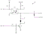
Referring to microcontroller U1 of fig. 9B, the microcontroller includes a transmit port XMIT and a receive port RCV. For transmission, the transmit XMIT line includes a circuit through resistor R13 and transistor Q3, and is connected to a port in connection point J1 labeled SDL (see fig. 9D). Referring to microcontroller U4 of fig. 8B, microcontroller U4 also includes transmit port XMIT and receive port RCV. For transmission, the transmit XMIT line includes a circuit through resistor R67 and transistor Q25, and is connected to a port in connection point J5 labeled SDL (see fig. 8D). It will be readily appreciated that additional circuit elements may be present in the transmission path, but the overall layout of the transmission path is similar.
Referring to the transmit path XMIT of fig. 9B and 9D, when the microcontroller U1 transmits logic 1(1), the transistor Q3 pulls current through the resistor R10, LED of the optocoupler U3 to ground. Similarly, transistor Q3 pulls current through resistor R52 and the LED of the optocoupler U10 of fig. 8D. The phototransistor of the optocoupler U10 turns on, pulling current through the resistor R68 and the optocoupler U10. The pulling of current through opto-coupler U10 causes a logic zero (0) to be registered on the receive port RCV of microcontroller U4. Thus, logic 1(1) at transmit port XMIT of microcontroller U1 of fig. 9B results in logic 0(0) at receive port RCV of microcontroller U4 of fig. 8B. The microcontrollers U1 and U4 are aware of this favorable transmission and one of the microcontrollers U1 or U4 can convert the result. Alternatively, an additional circuit may be added to the receive line to convert the result received from the optocoupler. The transmit port XMIT of microcontroller U4 and the receive port of microcontroller U1 may operate similarly.
Referring again to the transmission path XMIT of fig. 9B and 9D, when the microcontroller U1 transmits a logic zero (0), the transistor Q3 is non-conductive and no current is pulled through the LED of the optocoupler U3. Similarly, the transistor Q3 does not pull current through the resistor R52 and the LED of the optocoupler U10 of fig. 8B. The phototransistor of the optocoupler U10 is not conducting, so no current is pulled through the phototransistor of the optocoupler U10. The result is that logic 1(1) is registered on the receive port RCV of the microcontroller U4. Thus, logic 0(0) at transmit port XMIT of microcontroller U1 of fig. 9B results in logic 1(1) at receive port RCV of microcontroller U4 of fig. 8B. The microcontrollers U1 and U4 are aware of this supplemental transmission and one of the microcontrollers U1 or U4 may convert the result. The transmit port XMIT of microcontroller U4 and the receive port of microcontroller U1 may operate similarly.
Referring back to fig. 9D, as an example, resistors R10 and R12 limit the current through the LED of the photocoupler U3 to a safe level. Likewise, resistor R13 limits the current through the base connection of transistor Q3 to a safe level. When the transistor Q3 provides a not logic (1), the resistor R14 keeps the transistor Q3 off.
Including transistors Q3 and Q25 and opto couplers U3 and U10, coupled to the positive high voltage path (+ BAT) and the ground path (i.e., the low current path (COMM-) in fig. 8D and 9D), allow logic 0 (0)/logic 1(1) to be depicted for the respective controllers 300A and 300B. The relatively high current through the battery pack 330 and the cleaning system 100 does not affect the communication between the microcontroller U1 and the microcontroller U4.
A photocoupler, also called an opto-isolator or photocoupler, is a component that transmits an electrical signal between two isolated circuits by using light. The photocoupler prevents high voltage from affecting the system receiving the signal. Common types of opto-couplers (as shown in U3 and U10) include Light Emitting Diodes (LEDs) and phototransistors, which employ the same opaque encapsulation. Other types of light source sensor combinations include LED photodiodes, LED-LASCRs, and photoresistor pairs. Opto-couplers U3 and U10 transmit digital on/off (or logic 1/0) signals. The LEDs of the photocouplers U3 and U10 are two-lead semiconductor light sources. The phototransistor is a two-wire phototransistor that turns on in response to light from the LED. Although opto-couplers U3 and U10 are shown, alternative isolators, such as Radio Frequency (RF) couplers, may be used in place of opto-couplers U3 and U10.
Another detailed description of communication circuits 500 and 510 is provided below. The terminology used below with reference to fig. 8D and 9D is not meant to be limiting to fig. 8D and 9D. In contrast, fig. 8D and 9D disclose only one configuration described below.
Fig. 8D and 9D illustrate some embodiments of the battery pack 330 and power tool combination 100. Referring to fig. 8D, the battery pack 330 includes a first voltage source + BAT _ JMP, a second voltage source +3.3V, a first nominal voltage (ground), a first controller U4 having a first transmission terminal XMIT (see fig. 8B) and a first reception terminal RCV, and a first communication circuit 510. The first communication circuit 510 has a first data terminal SDL, a first isolation coupler U10 including a first input terminal 1, a second input terminal 2, a first output terminal 4, and a second output terminal 3. The first communication circuit also has a first transistor switch Q25 that includes a first terminal 3, a second terminal 2, and a first control terminal 1. The first voltage source + BAT JMP, the first input terminal 1 of the first isolation coupler U10, the second input terminal 2 of the first isolation coupler U10, the first terminal 3 of the first transistor switch Q25, the second terminal 2 of the first transistor switch Q25, and the first nominal voltage (ground) are electrically connected in a series configuration. The second voltage source 3.3V, the first output terminal 4 of the first isolating coupler U10, the second output terminal 3 of the first isolating coupler U10, and the first nominal voltage (ground) are electrically connected in a series configuration. A first transmission terminal XMIT of the first controller U4 is electrically connected to a first control terminal 1 of a first transistor switch Q25. A first receiving terminal RCV of the first controller U4 is electrically connected to the first input terminal 4 of the first isolating coupler U10. The first data terminal SDL is electrically connected between the second input terminal 2 of the first isolation coupler U10 and the first terminal 3 of the first transistor switch Q25.
As shown in fig. 9D, the electric power tool 100 has a third voltage source + BAT, a fourth voltage source +3.3V, a second nominal voltage (common), a second controller U1 (see fig. 9B) having a second transmission terminal 2 and a second reception terminal 3, and a second communication circuit 500. The second communication circuit 500 includes a second data terminal SDL and a second isolating coupler U3, the second isolating coupler U3 includes a third input terminal 1, a fourth input terminal 2, a third output terminal 4, and a fourth output terminal 3. The second communication circuit comprises a second transistor switch Q3 having a third terminal 3, a fourth terminal 2 and a second control terminal 1. The third voltage source + BAT, the third input terminal 1 of the second isolation coupler U3, the fourth input terminal 2 of the second isolation coupler U3, the third terminal 3 of the second transistor switch Q3, the fourth terminal 4 of the second transistor switch Q3, and the second nominal voltage (common) are electrically connected in a series configuration. The fourth voltage source 3.3V, the third output terminal 4 of the second isolating coupler U3, the fourth output terminal 3 of the second isolating coupler U4, and the second nominal voltage (common) are electrically connected in a series configuration. A second transmission terminal 3 of the second controller U1 is electrically connected to a second control terminal 1 of the second transistor switch Q3. The second receiving terminal 2 of the second controller U1 is electrically connected to the third input terminal 4 of the second isolating coupler U3. The second data terminal SDL is electrically connected between the fourth input terminal 2 of the second isolation coupler U3 and the third terminal 3 of the second transistor switch Q3. The first data terminal and the second data terminal are electrically connected.
Accordingly, the present invention provides a new and useful battery pack and cleaning system and method of operating the same. Various features and advantages of the invention are set forth in the following claims.