CN107919156B - Memory element and application thereof - Google Patents
Memory element and application thereof Download PDFInfo
- Publication number
- CN107919156B CN107919156B CN201610886837.XA CN201610886837A CN107919156B CN 107919156 B CN107919156 B CN 107919156B CN 201610886837 A CN201610886837 A CN 201610886837A CN 107919156 B CN107919156 B CN 107919156B
- Authority
- CN
- China
- Prior art keywords
- memory cells
- selecting
- write phase
- write
- level
- Prior art date
- Legal status (The legal status is an assumption and is not a legal conclusion. Google has not performed a legal analysis and makes no representation as to the accuracy of the status listed.)
- Active
Links
- 230000015654 memory Effects 0.000 title claims abstract description 289
- 238000000034 method Methods 0.000 claims description 21
- 238000009826 distribution Methods 0.000 description 58
- 238000003860 storage Methods 0.000 description 20
- 238000005516 engineering process Methods 0.000 description 15
- 238000010586 diagram Methods 0.000 description 12
- 239000010408 film Substances 0.000 description 10
- 239000004020 conductor Substances 0.000 description 7
- 239000000463 material Substances 0.000 description 7
- 239000004065 semiconductor Substances 0.000 description 7
- 239000002184 metal Substances 0.000 description 6
- 230000001965 increasing effect Effects 0.000 description 5
- 239000000758 substrate Substances 0.000 description 5
- 238000012795 verification Methods 0.000 description 5
- 238000003491 array Methods 0.000 description 3
- 229910021420 polycrystalline silicon Inorganic materials 0.000 description 3
- 229920005591 polysilicon Polymers 0.000 description 3
- 229910021332 silicide Inorganic materials 0.000 description 3
- FVBUAEGBCNSCDD-UHFFFAOYSA-N silicide(4-) Chemical compound [Si-4] FVBUAEGBCNSCDD-UHFFFAOYSA-N 0.000 description 3
- 230000000903 blocking effect Effects 0.000 description 2
- 230000008859 change Effects 0.000 description 2
- 239000003795 chemical substances by application Substances 0.000 description 2
- 238000013500 data storage Methods 0.000 description 2
- 239000006185 dispersion Substances 0.000 description 2
- 238000007667 floating Methods 0.000 description 2
- 238000004519 manufacturing process Methods 0.000 description 2
- 230000008569 process Effects 0.000 description 2
- 239000010409 thin film Substances 0.000 description 2
- 230000005641 tunneling Effects 0.000 description 2
- 108091093105 Nuclear DNA Proteins 0.000 description 1
- 238000004364 calculation method Methods 0.000 description 1
- 230000000052 comparative effect Effects 0.000 description 1
- 230000008878 coupling Effects 0.000 description 1
- 238000010168 coupling process Methods 0.000 description 1
- 238000005859 coupling reaction Methods 0.000 description 1
- 230000002542 deteriorative effect Effects 0.000 description 1
- 230000005684 electric field Effects 0.000 description 1
- 230000001939 inductive effect Effects 0.000 description 1
- 239000011810 insulating material Substances 0.000 description 1
- 238000012986 modification Methods 0.000 description 1
- 230000004048 modification Effects 0.000 description 1
- 229910021421 monocrystalline silicon Inorganic materials 0.000 description 1
- 230000004044 response Effects 0.000 description 1
- 229910052710 silicon Inorganic materials 0.000 description 1
- 239000010703 silicon Substances 0.000 description 1
- 239000007787 solid Substances 0.000 description 1
- 230000007480 spreading Effects 0.000 description 1
- 238000003892 spreading Methods 0.000 description 1
Images


Classifications
-
- G—PHYSICS
- G11—INFORMATION STORAGE
- G11C—STATIC STORES
- G11C16/00—Erasable programmable read-only memories
- G11C16/02—Erasable programmable read-only memories electrically programmable
- G11C16/06—Auxiliary circuits, e.g. for writing into memory
- G11C16/10—Programming or data input circuits
-
- H—ELECTRICITY
- H10—SEMICONDUCTOR DEVICES; ELECTRIC SOLID-STATE DEVICES NOT OTHERWISE PROVIDED FOR
- H10B—ELECTRONIC MEMORY DEVICES
- H10B41/00—Electrically erasable-and-programmable ROM [EEPROM] devices comprising floating gates
- H10B41/20—Electrically erasable-and-programmable ROM [EEPROM] devices comprising floating gates characterised by three-dimensional arrangements, e.g. with cells on different height levels
- H10B41/23—Electrically erasable-and-programmable ROM [EEPROM] devices comprising floating gates characterised by three-dimensional arrangements, e.g. with cells on different height levels with source and drain on different levels, e.g. with sloping channels
- H10B41/27—Electrically erasable-and-programmable ROM [EEPROM] devices comprising floating gates characterised by three-dimensional arrangements, e.g. with cells on different height levels with source and drain on different levels, e.g. with sloping channels the channels comprising vertical portions, e.g. U-shaped channels
-
- H—ELECTRICITY
- H10—SEMICONDUCTOR DEVICES; ELECTRIC SOLID-STATE DEVICES NOT OTHERWISE PROVIDED FOR
- H10B—ELECTRONIC MEMORY DEVICES
- H10B43/00—EEPROM devices comprising charge-trapping gate insulators
- H10B43/20—EEPROM devices comprising charge-trapping gate insulators characterised by three-dimensional arrangements, e.g. with cells on different height levels
- H10B43/23—EEPROM devices comprising charge-trapping gate insulators characterised by three-dimensional arrangements, e.g. with cells on different height levels with source and drain on different levels, e.g. with sloping channels
- H10B43/27—EEPROM devices comprising charge-trapping gate insulators characterised by three-dimensional arrangements, e.g. with cells on different height levels with source and drain on different levels, e.g. with sloping channels the channels comprising vertical portions, e.g. U-shaped channels
Landscapes
- Semiconductor Memories (AREA)
- Non-Volatile Memory (AREA)
Abstract
一种存储器元件的两侧步进写入操作,此存储器元件包括具有多个存储单元C1(i)的第一叠层结构和多个存储单元C2(i)存储器的第二叠层结构。i代表存储单元的阶层。步进写入操作包括对第一叠层结构和第二叠层结构的存储单元施加初步写入阶段S1、中间写入阶段S2以及最终写入阶段S3。根据写入顺序,使最终写入阶段S3可在第一叠层结构和第二叠层结构目标阶层(i)中的目标存储单元上实施;且使位于目标阶层(i)的邻接阶层(i+1和i‑1)上的邻接存储单元已经先实施过中间写入阶段S2。其中,中间写入阶段S2实施于该第一叠层结构和该第二叠层结构中目标阶层(i)的存储单元,且邻接阶层(i+1和i‑1)已经先实施过初步写入阶段S1于这些邻接存储单元上。
A two-sided step-write operation of a memory element, the memory element includes a first stacked structure having a plurality of memory cells C1(i) and a second stacked structure of a memory having a plurality of memory cells C2(i). i represents the level of the memory cell. The step-write operation includes applying a preliminary write stage S1, an intermediate write stage S2, and a final write stage S3 to the memory cells of the first stacked structure and the second stacked structure. According to the write sequence, the final write stage S3 can be implemented on the target memory cells in the target level (i) of the first stacked structure and the second stacked structure; and the adjacent memory cells located on the adjacent levels (i+1 and i-1) of the target level (i) have already been implemented with the intermediate write stage S2. The intermediate write stage S2 is implemented on the memory cells of the target level (i) in the first stacked structure and the second stacked structure, and the adjacent levels (i+1 and i-1) have already been implemented with the preliminary write stage S1 on these adjacent memory cells.
Description
技术领域technical field
本发明是有关于一种高密度存储器元件,特别是有关于一种具有多存储单元平面层(multiple planes of memory cells)且排列来提供立体阵列的存储器元件。The present invention relates to a high-density memory device, and more particularly, to a memory device having multiple planes of memory cells arranged to provide a three-dimensional array.
背景技术Background technique
随着集成电路的关键尺寸微缩至存储单元技术的一般极限,设计者开始寻求以叠层的多层存储单元平面层技术,来达到增进储存效能及降低位成本(costs per bit)的目的。例如,Lai et al.,“A Multi-Layer Stackable Thin-Film Transistor(TFT)NAND-Type Flash Memory,”IEEE Int′l Electron Devices Meeting,11-13Dec.2006以及Junget al.,“Three Dimensionally Stacked NAND Flash Memory Technology UsingStacking Single Crystal Si Layers on ILD and TANOS Structure for Beyond 30nmNode,”IEEE Int′l Electron Devices Meeting,11-13Dec.2006提出将薄膜晶体管技术应用于电荷捕捉存储技术中。As the critical dimensions of integrated circuits shrink to the general limits of memory cell technology, designers have begun to seek stacked multi-level memory cell plane layer technology to improve storage performance and reduce costs per bit. For example, Lai et al., "A Multi-Layer Stackable Thin-Film Transistor (TFT) NAND-Type Flash Memory," IEEE Int'l Electron Devices Meeting, 11-13Dec.2006 and Jung et al., "Three Dimensionally Stacked NAND Flash Memory Technology Using Stacking Single Crystal Si Layers on ILD and TANOS Structure for Beyond 30nmNode, "IEEE Int'l Electron Devices Meeting, 11-13Dec.2006 proposed to apply thin film transistor technology to charge trapping storage technology.
Katsumata et al.,“Pipe-shaped BiCS Flash Memory with 16Stacked Layersand Multi-Level-Cell Operation for Ultra High Density Storage Devices,”2009Symposium on VLSI Technology Digest of Technical Papers,2009.则提出另一种结构,提供一种应用电荷捕捉存储技术的垂直NAND存储单元。Katsumata et al.所描述的结构包括一个垂直U形NAND存储器,并使用硅-硅氧化物-氮化硅-硅氧化物-硅(silicon-oxide-nitride-oxide-silicon,SONOS)的电荷捕捉技术,在每一个栅极/垂直通道接口(gate/vertical channel interface)上形成存储储位(memory sites)。此一存储器结构是以一个用来作为NAND栅极的垂直通道的U形半导体材料线、一个位于U形半导体材料线的一端顶部上方阶层的选择栅极(upper select gate)以及一个位于U形半导体材料线的另一端顶部上方阶层的接地选择栅极或源极侧选择栅极作为基础。多条使用平面字符线层所构成的水平字符线(horizontal word lines)与该U形半导体材料的每端相交处从而在各端每一阶层中形成所谓的栅极围绕式(gate-all-around)存储单元。Katsumata et al., "Pipe-shaped BiCS Flash Memory with 16Stacked Layers and Multi-Level-Cell Operation for Ultra High Density Storage Devices," 2009Symposium on VLSI Technology Digest of Technical Papers, 2009. proposed another structure, providing a Vertical NAND memory cell using charge trapping storage technology. The structure described by Katsumata et al. includes a vertical U-shaped NAND memory and uses a silicon-oxide-nitride-oxide-silicon (SONOS) charge trapping technology , and memory sites are formed on each gate/vertical channel interface. This memory structure is composed of a U-shaped line of semiconductor material used as a vertical channel for the NAND gate, an upper select gate on top of one end of the U-shaped line of semiconductor material, and a U-shaped semiconductor line A grounded select gate or source side select gate of a level above the top of the other end of the line of material serves as the base. A plurality of horizontal word lines formed using planar word line layers intersect each end of the U-shaped semiconductor material to form a so-called gate-all-around at each end and in each level. ) storage unit.
U形NAND结构具有存储单元叠层结构(stacks of cells),例如位于每一个U形半导体材料线的端上彼此设置得非常靠近的存储单元。其他的立体结构同样也具有设置得非常靠近的存储单元叠层结构。在密集的结构中,为了对存储单元进行写入或抹除操作所产生的电场(electric field)和热场(thermal fields)干扰,可能来自于同一个叠层结构或邻近的叠层结构。The U-shaped NAND structure has stacks of cells, such as memory cells located very close to each other on the end of each U-shaped line of semiconductor material. Other three-dimensional structures also have stacks of memory cells arranged in close proximity. In a dense structure, the electric field and thermal fields generated by the writing or erasing operation of the memory cells may come from the same stack structure or adjacent stack structures.
Katsumata et al.指出此一结构可采用多位写入(multiple-bit-per-cellprogramming)技术来实施。多位写入技术需要对数以千计的控制电压作完善的控制,这使得读取和写入干扰特性变得更加重要。因此,即便采用立体快闪技术度,但是其数据储存密度仍然有所限制。Katsumata et al. pointed out that such a structure can be implemented using multiple-bit-per-cell programming techniques. Multi-bit write techniques require sophisticated control over thousands of control voltages, making read and write disturb characteristics even more important. Therefore, even if the stereo flash technology is adopted, its data storage density is still limited.
因此,有需要提供一种制作成本低、稳定、记忆单元小且高数据密度的立体集成电路存储器结构,并提供一种可降低写入抹除干扰的技术。Therefore, there is a need to provide a 3D integrated circuit memory structure with low manufacturing cost, stability, small memory cells and high data density, and a technique for reducing write-erase interference.
发明内容SUMMARY OF THE INVENTION
用来进行两侧步进写入操作(two-sided,staged programming operation)的立体存储器元件,例如U形NAND串行的立体NAND闪存(3D NAND flash with U-shaped NANDstrings),具有基于存储单元实体阶层的顺序,且被应用于紧密间隔的存储单元叠层结构中。这种存储器元件具有由存储单元C1(i)构成的第一叠层结构以及由存储单元C2(i)构成的第二叠层结构。在多个阶层中,i代表一个标号(index),用来索引叠层结构中某存储单元的阶层。其中,i由1到N。步进写入操作包括根据写入顺序(programming order),针对位于第一叠层结构及第二叠层结构中的存储单元实施初步写入阶段(preliminary programstage)S1、中间写入阶段(intermediate program stage)S2和最终写入阶段(finalprogram stage)S3。Three-dimensional memory devices for two-sided, staged programming operations, such as 3D NAND flash with U-shaped NAND strings, have memory cell-based entities The sequence of levels is applied in a closely spaced stack of memory cells. This memory element has a first stacked structure composed of memory cells C1(i) and a second stacked structure composed of memory cells C2(i). In multiple levels, i represents an index, which is used to index the level of a memory cell in the stacked structure. where i ranges from 1 to N. The step-by-step writing operation includes performing a preliminary program stage S1 and an intermediate writing stage (intermediate program) for the memory cells located in the first stacked structure and the second stacked structure according to the programming order. stage) S2 and final program stage S3.
写入顺序的编排是,当在第一叠层结构及第二叠层结构的每一阶层(i)的存储单元中实施最终写入阶段S3时。最终写入阶段S3实施于第一叠层结构及第二叠层结构中该目标阶层(i)的存储单元,且邻近阶层(i+1或i-1)已经先实施过该中间写入阶段S2于该些邻接存储单元上。同时,中间写入阶段S2只会在位于第一叠层结构及第二叠层结构的邻近阶层(i+1或i-1)中已经先实施过初步写入阶段S1的存储单元上实施。The programming of the writing sequence is when the final writing stage S3 is performed in the memory cells of each level (i) of the first and second stacked layers. The final writing stage S3 is performed on the memory cells of the target level (i) in the first and second stacked structures, and the intermediate writing stage has already been performed on the adjacent level (i+1 or i-1) S2 is on the adjacent memory cells. Meanwhile, the intermediate writing stage S2 is only implemented on the memory cells located in the adjacent layers (i+1 or i-1) of the first stacked structure and the second stacked structure, which have already performed the preliminary writing stage S1.
此处所述的存储器元件包括实施写入操作的电路。The memory elements described herein include circuitry to perform write operations.
本技术的其他层面及优点,可见于下述的图式、说明书及申请专利范围,其详细说明如下:Other aspects and advantages of this technology can be found in the following drawings, descriptions and the scope of the patent application, which are described in detail as follows:
附图说明Description of drawings
图1是根据现有技术所绘示的一种闪存NAND串行的简化电路图。FIG. 1 is a simplified circuit diagram of a flash NAND string according to the prior art.
图2是根据现有技术绘示一组存储单元在所谓三阶段写入方法的三种阶段的临界电压分布图。FIG. 2 is a diagram illustrating threshold voltage distributions of a group of memory cells in three stages of a so-called three-stage writing method according to the prior art.
图3是根据现有技术绘示对NAND串行实施三阶段写入方法时的写入序列。FIG. 3 illustrates a write sequence when a three-stage write method is implemented for NAND strings according to the prior art.
图4是绘示位于立体NAND结构的单一柱状主动体中的U形NAND串行电路图。FIG. 4 is a circuit diagram illustrating a U-shaped NAND string in a single column active body of a three-dimensional NAND structure.
图5是绘示立体NAND结构中具有U形垂直通道NAND串行的柱状主动体的结构剖面图。5 is a cross-sectional view illustrating the structure of a columnar active body having a U-shaped vertical channel NAND string in a three-dimensional NAND structure.
图6是绘示立体NAND结构中具有U形垂直通道NAND串行以与栅极围绕式字符线结构的剖面示意图。6 is a schematic cross-sectional view illustrating a U-shaped vertical channel NAND string and a gate-surrounding wordline structure in a three-dimensional NAND structure.
图7是绘示位于目标U形NAND串行上的存储单元以及位于邻近U形NAND串行上的存储单元之间的写入脉冲值与临界电压的关系曲线的变化图。FIG. 7 is a graph showing the relationship between the write pulse value and the threshold voltage between the memory cells located on the target U-shaped NAND string and the memory cells located on the adjacent U-shaped NAND strings.
图8和图9分别绘示一种临界电压与存储单元数量关系图,分别显示在实施现有写入操作之后,U形NAND串行的源极侧和漏极侧的临界电压分布。FIG. 8 and FIG. 9 are respectively a graph showing the relationship between the threshold voltage and the number of memory cells, respectively showing the distribution of the threshold voltage on the source side and the drain side of the U-shaped NAND string after performing the conventional write operation.
图10A至图10X是根据本说明书的实施例所绘示的两侧步进写入操作的结构剖面图。10A to FIG. 10X are structural cross-sectional views of a two-side step write operation according to an embodiment of the present specification.
图11和图12是绘示一种临界电压与存储单元数量关系图,显示在实施两侧阶段步进写入操作及现有写入操作之后,U形NAND串行的对比临界电压分布图。FIGS. 11 and 12 are graphs showing the relationship between threshold voltage and the number of memory cells, showing the comparative threshold voltage distributions of U-shaped NAND strings after performing a two-sided step step write operation and a conventional write operation.
图13是绘示一种包含有于U形NAND串行的立体存储器串行的集成电路存储器方块图。13 is a block diagram illustrating an integrated circuit memory including a three-dimensional memory string in a U-shaped NAND string.
【符号说明】【Symbol Description】
11、12:晶体管11, 12: Transistors
14、15、16、17、70、71、86、87:存储单元14, 15, 16, 17, 70, 71, 86, 87: storage units
20、20’、21、22、23、24、26、27、28:临界电压分布状态20, 20', 21, 22, 23, 24, 26, 27, 28: critical voltage distribution state
50:垂直通道结构 51a、51b:通道本体的部分50:
52:绝缘基材层 53:缝隙52: Insulating substrate layer 53: Gap
56、57、62、63:高导电性薄膜 58、59:字符线条带56, 57, 62, 63: Highly
60、61:辅助栅极线 69:电荷储存单元60, 61: auxiliary gate line 69: charge storage unit
81-B:导体 81-1、81-2:柱状主动体81-B: Conductor 81-1, 81-2: Columnar active body
82:电荷储存单元 94、95:导线82:
100:基材 101:通道线100: Substrate 101: Channel Line
128:共同源极线接触 129:位线接触128: Common source line contact 129: Bit line contact
131:接地选择开关 132:串行选择开关131: Ground selector switch 132: Serial selector switch
134:NAND串行的底部 135、AG:辅助栅极结构134: Bottom of
152、153:参考线152, 153: Reference lines
160、161、SP、EV、PV1至PV7、ERS:曲线160, 161, SP, EV, PV1 to PV7, ERS: Curve
901:集成电路 905:数据总线901: Integrated Circuits 905: Data Buses
930:总线 910:控制逻辑930: Bus 910: Control Logic
920:偏压配置电压源 940:串行选择线/接地选择线行译码器920: Bias Configuration Voltage Source 940: Serial Select Line/Ground Select Line Row Decoder
945:串行选择线/接地选择线 950:字符线阶层译码器945: Serial Select Line/Ground Select Line 950: Word Line Hierarchy Decoder
955:单数/偶数字符线 960:立体存储器阵列955: odd/even word lines 960: stereo memory array
965:全局位线 970:全局位线列译码器965: Global Bit Line 970: Global Bit Line Column Decoder
971:源极线译码器 975:第一数据线971: Source Line Decoder 975: First Data Line
980:感测放大器/写入缓冲电路 985:第二数据线980: Sense Amplifier/Write Buffer Circuit 985: Second Data Line
990:多阶层数据缓冲器 991:输入/输出电路990: Multi-level data buffer 991: Input/output circuit
993:线数据路径 BL:字符线993: Line Data Path BL: Word Line
SL:源极线 GSL:接地选择线SL: Source Line GSL: Ground Select Line
SSL:串行选择线 S1:初步写入阶段SSL: Serial Select Line S1: Preliminary Write Phase
S2:中间写入阶段 S3:最终写入阶段S2: Intermediate write stage S3: Final write stage
88、89、WL1、WL2、WL3、WL4、WLS1(1)至WLS1(N)、WLS2(1)至WLS2(N)、G(0)至G(2N-1):字符线(栅极)88, 89, WL1, WL2, WL3, WL4, WLS1(1) to WLS1(N), WLS2(1) to WLS2(N), G(0) to G(2N-1): Word Line (Gate)
具体实施方式Detailed ways
本说明书的实施例是配合图1至图13所绘示的图式来进行说明。图1是绘示一种基础二维快闪NAND串行的电路图。此NAND串行包括位于字符线BL和源极线SL之间,彼此串联的多个存储单元晶体管。由晶体管11所构成的第一开关,连接字符线BL和串行的一端,从而响应串行选择线SSL的信号。由晶体管12所构成的第二开关,将串行的相反一端连接至源极线SL,从而响应接地选择线GSL的信号。存储单元14、15、16和17排列并彼此串联在第一开关和第二开关之间。在一条给定的串行中,当然也可以有更多数目的存储单元。The embodiments of this specification are described with reference to the drawings shown in FIGS. 1 to 13 . FIG. 1 is a circuit diagram illustrating a basic two-dimensional flash NAND string. This NAND string includes a plurality of memory cell transistors connected in series with each other between the word line BL and the source line SL. The first switch formed by the
当在NAND串行中对每一个存储单元进行多位储存(multiple bits per cell)时,是施加偏压安排(bias arrangement)来控制目标存储单元的电荷捕捉结构中被捕捉的电荷数量,从而设定位于某一阶层的目标存储单元中用来对应特定数据(data)的临界电压。例如一个储存三个位数据的存储单元,会被构建来设定8个范围,分别代表存储单元中这三个位的8种组合。为了进行存储单元的多位储存,必须精准控制每一种存储状态(memorystates)的临界电压分布。When performing multiple bits per cell for each memory cell in a NAND string, a bias arrangement is applied to control the amount of charge trapped in the charge trapping structure of the target memory cell, thereby setting Threshold voltage used to correspond to specific data (data) in target memory cells located at a certain level. For example, a memory cell that stores three bits of data will be constructed to set 8 ranges, representing 8 combinations of the three bits in the memory cell. In order to perform multi-bit storage of memory cells, the threshold voltage distribution of each memory state must be precisely controlled.
为了进行NAND串行的存储单元多位储存,发展出增量步进脉冲写入(incrementalstep pulsed programming,ISPP)技术。其包含施加写入脉冲至被选定的存储单元的字符线,以及对被选定的NDND串行的源极端和位线端施加对应的偏压,从而诱发电荷穿隧。之后,进行临界电压验证步骤,假如验证不通过,再重复一次。写入脉冲的量是逐步增加,或者通过脉冲/验证循环来变动,直到达成存储单元的目标临界电压。增量步进脉冲写入容许对所达成的目标临界电压进行精准控制。然而,为了使NAND串行得到较高的储存密度,存储单元中的电荷储存结构会实质连接。因此,写入操作施加的偏压会而横跨整个阵列。存储单元的临界电压会被邻近存储单元的写入操作所干扰,造成存储单元的临界电压分布分散(spreading of the threshold voltage distributions),导致读取极限(read margin)降低。相同的写入过程,包含写入脉冲/验证循环,也可以施加在其他形态的存储器中,包括可写入电阻式存储器(programmable resistance memory)。In order to perform multi-bit storage of NAND serial memory cells, incremental step pulsed programming (ISPP) technology is developed. It includes applying write pulses to the word lines of selected memory cells, and applying corresponding bias voltages to the source and bit line terminals of the selected NDND strings, thereby inducing charge tunneling. After that, perform the threshold voltage verification step, and if the verification fails, repeat it again. The amount of write pulses is incrementally increased, or varied through pulse/verify cycles, until the target threshold voltage of the memory cell is reached. Incremental step pulse writing allows precise control of the target threshold voltage achieved. However, in order to achieve higher storage density for NAND strings, the charge storage structures in the memory cells are substantially connected. Therefore, the bias voltage applied by the write operation will span the entire array. The threshold voltages of the memory cells are disturbed by the write operation of the adjacent memory cells, resulting in spreading of the threshold voltage distributions of the memory cells, resulting in lower read margins. The same write process, including write pulse/verify cycles, can also be applied to other forms of memory, including programmable resistance memory.
降低写入操作对邻近存储单元的干扰的其中一种做法,称作三阶段写入(three-step programming,TSP)运算的方法,目前已经被发展出来,可用来降低闪存临界电压分布的分散。One of the methods to reduce the interference of write operations to adjacent memory cells, a method called three-step programming (TSP) operation, has been developed to reduce the dispersion of flash threshold voltage distribution.
图2是绘示一种三阶段写入操作。包括可形成如上方图所示的二进制临界电压分布状态(binary threshold voltage distribution state)的“二进制”阶段("binary"stage)、可形成如中间图所示的模糊多电平临界电压分布状态(“foggy”multilevelthreshold voltage distribution state)的模糊阶段(“foggy”stage)以及可行成如下方图所示的完善多电平临界电压分布状态(“fine”multilevel threshold voltagedistribution state)的完善阶段(“fine”stage)。FIG. 2 illustrates a three-stage write operation. Including a "binary" stage, which can form a binary threshold voltage distribution state as shown in the upper figure, a fuzzy multi-level threshold voltage distribution state as shown in the middle figure ( The fuzzy stage ("foggy" stage) of the "foggy" multilevel threshold voltage distribution state) and the perfect stage ("fine" stage) that can be made into the perfect multilevel threshold voltage distribution state ("fine" multilevel threshold voltage distribution state) as shown in the following figure stage).
此一写入操作包括一个写入序列(programming sequence)。首先进行二进制阶段,先对存储单元进行预抹除(pre-erased),然后进行一个具有单一验证临界值(verifythreshold)的写入操作。在写入操作的二进制阶段之后,阵列中未被写入的存储单元保持抹除状态,并且具有临界电压分布状态20。阵列中被施加写入脉冲的存储单元的临界电压,则增加至临界电压分布状态21,如写入操作的二进制阶段的结果。This write operation includes a programming sequence. The binary stage is performed first, where the memory cells are pre-erased, followed by a write operation with a single verify threshold. After the binary phase of the write operation, unwritten memory cells in the array remain in the erased state and have a threshold
接着写入序列进行模糊阶段,其中保持抹除状态的存储单元维持稍微变宽的临界电压分布状态20′。要被写入至具有三种写入电平的存储单元,其临界电压从被抹除的临界电压分布状态20扩大至中间程度的临界电压分布状态其中之一,例如临界电压分布状态22或临界电压分布状态23。二进制阶段之后一开始即具有临界电压分布状态21的存储单元,其临界电压则增加至高电平的临界电压分布状态,例如临界电压分布状态24。上述操作可以采用增量步进脉冲写入序列,通过用来建立七个上述临界电压分布状态的七种临界电平或其他算法来达成。在此中间阶段所进行的序列中,可以对每个脉冲/验证周期施加幅度相对较大的增量,因此操作的速度相对较快,使用数目相对较少的脉冲/验证周期。然而,较大幅度的增量会导致因为进行中间阶段所产生的状态,具有相对较宽的临界电压范围。The write sequence then proceeds to a blur phase in which the memory cells remaining in the erased state maintain a slightly wider threshold voltage distribution state 20'. To be written to a memory cell with three write levels, its threshold voltage is expanded from the erased threshold
最后,写入序列进行完善阶段。在完善阶段中,存储单元会被调整成完善状态,使其具有较窄的临界电压分布和较宽的幅度范围(margin)。因此,可以收紧模糊阶段中具有临界电压分布状态22的存储单元的临界电平,而变成完善阶段的临界电压分布状态26。同样地,可以收紧模糊阶段中具有临界电压分布状态23的存储单元的临界电平,而变成完善阶段的分布状态27。同样地,可以收紧模糊阶段中具有临界电压分布状态24的存储单元的临界电平,而变成完善阶段的临界电压分布状态28。Finally, the write sequence goes through the refinement phase. In the perfecting stage, the memory cells are adjusted to a perfected state with a narrower threshold voltage distribution and a wider margin. Therefore, the threshold level of the memory cell having the threshold
总体而言,图2所绘示的临界电压分布状态显示了一种用来对每一个存储单元进行多位数据写入的典型实施例。In general, the threshold voltage distribution shown in FIG. 2 shows a typical embodiment for writing multi-bit data to each memory cell.
为了降低写入程序中所产生的干扰,写入阶段中NDNA串行单元的顺序,可以采用如图3所绘示的方式加以控制。图3是绘示对图1所示具有四条字符线的NAND串行实施三阶段写入方法时的写入序列。此处所述的写入序列包括,先对字符线WL1进行二进制阶段操作,使存储单元具有一个二进制状态。接着,对字符线WL2进行二进制阶段操作。然后,写入序列,对字符线WL1进行模糊阶段操作,并对字符线WL3进行二进制阶段操作。之后,对字符线WL2进行模糊阶段操作,对字符线WL1进行完善阶段操作。In order to reduce the interference generated in the writing process, the sequence of the NDNA serial units in the writing stage can be controlled in the manner shown in FIG. 3 . FIG. 3 illustrates a write sequence when a three-stage write method is implemented on the NAND string with four word lines shown in FIG. 1 . The write sequence described here includes first performing a binary phase operation on the word line WL1 so that the memory cell has a binary state. Next, a binary phase operation is performed on word line WL2. Then, the sequence is written to perform a blur phase operation on word line WL1 and a binary phase operation on word line WL3. After that, the blurring stage operation is performed on the word line WL2, and the perfecting stage operation is performed on the word line WL1.
Li等人,在"128Gb 3b/Cell NAND Flash Memory in 19nm Technology with18MB/s Write Rate and 400Mb/s Toggle Mode",IEEE International Solid-StateCircuits Conference,2012.中提及了三阶段写入(three-step programming,TSP)技术。Li et al., "128Gb 3b/Cell NAND Flash Memory in 19nm Technology with 18MB/s Write Rate and 400Mb/s Toggle Mode", IEEE International Solid-State Circuits Conference, 2012. mentioned three-stage writing programming, TSP) technology.
随着新的存储器结构被发展出来,在一些新的结构中,三阶段写入技术并无法解决写入操作中在存储单元彼此之间所产生的干扰(cell-to-cell disturbance)问题。例如,由于存储单元的实体结构会产生更复杂的写入电压耦合(coupling of the programvoltages),因此即便使用三阶段写入技术,具有U形串行的NAND的立体结构仍然因为前述的干扰,而面临临界电压分布分散的问题。As new memory structures are developed, in some new structures, the three-stage write technology cannot solve the problem of cell-to-cell disturbance generated between memory cells during write operations. For example, since the physical structure of the memory cell will generate more complicated coupling of the program voltages, even if the three-stage writing technology is used, the three-dimensional structure of the NAND with U-shaped serial is still due to the aforementioned disturbance. Faced with the problem of dispersion of critical voltage distribution.
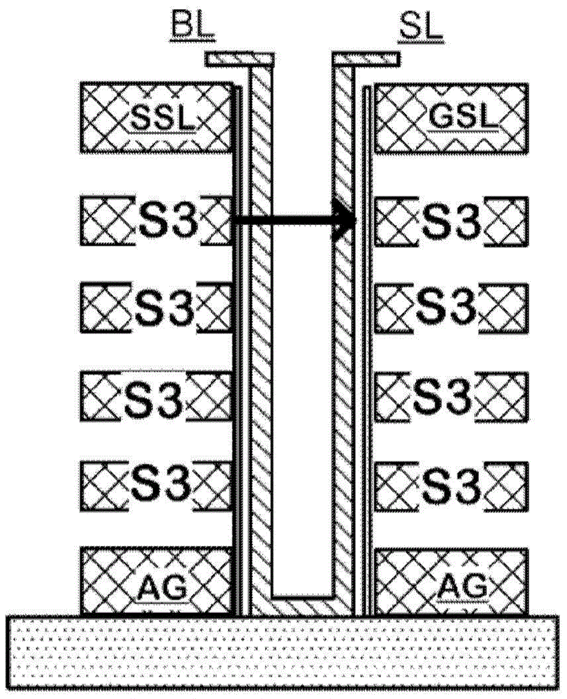
图4是绘示一种U形NAND串行的电路图。此种U形NAND串行是多个快闪存储单元,以串连的方式连接于串行选择开关132(有时称之为漏极侧开关)和接地选择开关131(有时称之为源极侧开关)。其中,串行选择开关132连接至位线接触129;接地选择开关131连接至共同源极线接触128。U形NAND串行垂直地位于立体结构之中,并且具有两个位于两边的通道线的存储单元叠层结构,本文中分别称之为第一叠层结构和第二叠层结构。在本实施例之中,第一叠层结构的上方阶层包括一条接地选择线GSL,在NAND串行中是用来作为第一(接地选择)开关131的栅极。第二叠层结构的上方阶层包括一条串行选择线SSL,在NAND串行中是用来作为第二(串行选择)开关132的栅极。在叠层结构的中间阶层中,包括多条字符线。位于第一叠层结构中的字符线,包括字符线WLS1(1)至字符线WLS1(N),其中,标号1至N代表该字符线位于第一叠层结构中相对的实体阶层位置。位于第二叠层结构中的字符线,包括字符线WLS2(1)至字符线WLS2(N)。U形NAND串行的底部134与通道线(又称为区域位线)电性连接,例如二者由单一的连续膜层所构成。(虽然在一些实施例中可能会省略)在本实施例中还包括一个辅助栅极结构135,通过一个栅介电层连接至位于上述叠层结构底部的通道在线。辅助栅极结构135可以用来诱发反转区(inversion region),从而增进通道的第一端和第二端之间的导电性。NAND串行中的字符线是用来作为串行中存储单元的栅极,且通常使用0到少于串行中存储单元数量的标号来表示之。在本实施例之中,U形NAND串行具有2N个存储单元。其中,N代表阶层的数目;标号G(0)至G(2N-1)分别代表字符线。位于第一侧的字符线包括G(0)至G(N-1)。位于第二侧的字符线包括G(N)至G(2N-1)。FIG. 4 is a circuit diagram illustrating a U-shaped NAND string. This U-shaped NAND string is a plurality of flash memory cells connected in series to a string select switch 132 (sometimes called a drain side switch) and a ground select switch 131 (sometimes called a source side switch) switch). Among them, the
图5是绘示用来实施图4的U形垂直通道NAND串行的柱状主动体的结构剖面图。有关U形垂直通道NAND串行的结构和制作方法,可以参照与本案具有共同发明人编号为US14/637,204,申请日为2015年3月3日,发明名称为“U-Shaped Vertical Thin-ChannelMemory”的美国专利申请案。而该前案的内容将通过引用并入的方式,全文机载于本说明书之中。图5中的柱状主动体包括垂直通道结构50,垂直通道结构50包含垂直多晶硅半导体本体,包含被缝隙53沿着柱状体长度方向隔离的奇数和偶数薄层通道膜;且垂直通道结构50电性连接至位于绝缘基材层52上的柱状主动体底部。电荷储存单元69置于柱状主动体的每一侧。垂直通道结构50包括一个用来对位于一侧边的串行选择线晶体管提供通道本体的部分51a以及一个用来对位于另一侧边的接地选择线晶体管提供通道本体的部分51b。缝隙53位于部分51a和51b以及垂直通道结构50底部之间,且位于垂直通道结构50的字符线的第一和第二叠层结构之间。FIG. 5 is a cross-sectional view illustrating the structure of a columnar active body used to implement the U-shaped vertical channel NAND string of FIG. 4 . For the structure and manufacturing method of U-shaped vertical channel NAND serial, please refer to the co-inventor number US14/637,204 with the present case, the filing date is March 3, 2015, and the invention name is "U-Shaped Vertical Thin-ChannelMemory" US patent application. The content of the preceding case will be incorporated by reference, and the full text is contained in this specification. The columnar active body in FIG. 5 includes a
在图5所绘示的结构中,存储单元位于垂直通道结构50和字符线的交叉处。例如,第一叠层结构中的存储单元70和71是位于字符线条带58和59所在的阶层与垂直通道结构50的交叉处。存储单元70和71分别独立地被字符线条带58和59的信号所开闭(gated)。In the structure shown in FIG. 5, the memory cells are located at the intersections of the
图5绘示导电条带54和55,分别构建来作为串行选择线SSL和接地选择线GSL,二者均位于导电条带叠层结构的上方阶层。用来作为选择线的导电条带54和55,还可以包括位于其外表面上方的高导电性薄膜56和57。例如,可以是金属硅化物薄膜。FIG. 5 shows
图5同时还绘示辅助栅极线60和61,可以来作为包含字符线的叠层结构中的导电条带。辅助栅极线60和61还可以包括位于其外表面上方的高导电性薄膜62和63。例如,可以是金属硅化物薄膜。FIG. 5 also shows
同样的,导电条带可以配置成位于垂直通道结构50的相反两侧的第一和第二字符线叠层结构。第一字符线叠层结构包括字符线WLS1(1)至WLS1(N)。第二字符线叠层结构包括字符线WLS2(1)至WLS2(N)。因此,导电条带59是位于第一字符线叠层结构的第3阶层的字符线WLS1(3);导电条带58是位于第二字符线叠层结构的第3阶层的字符线WLS2(3)。第一和第二字符线叠层结构具有N个阶层。在本实施例中,如图所示,N等于8。当然,也可以采用不同数目,例如16、32或更大数目的字符线阶层。Likewise, the conductive strips may be configured as first and second wordline stacks on opposite sides of the
图5所绘示,字符线可以包含位于其外表面上方的金属硅化物薄膜或其他高导电性薄膜(例如高导电性薄膜62)。As shown in FIG. 5, the wordline may include a metal silicide film or other highly conductive film (eg, highly conductive film 62) over its outer surface.
在其他实施例之中,所有的或部分的串行选择线、字符线、接地选择线是使用金属或其他非多晶硅的导电材料来加以实施。In other embodiments, all or part of the serial select lines, word lines, ground select lines are implemented using metal or other conductive materials other than polysilicon.
图5所绘示的结构提供位于垂直通道结构50的相奇数和偶数侧的独立电荷储存位(charge storage sites)。同时,此结构提供了沿着垂直通道结构50的相反两侧延伸的单一U形垂直通道NAND串行。The structure shown in FIG. 5 provides independent charge storage sites on the odd and even sides of the
参考线结构,例如位于图案化金属层中的导线,可以正交地排列于导电条带叠层结构上方,并在源极线接触SL上与柱状主动体电性连接,从而通过位于源极侧的开关来施加偏压。位线结构,例如位于图案化金属层中的导线,可以正交地排列于奇数和偶数导电条带叠层结构上方,并在位线接触BL上与柱状主动体电性连接,从而通过位于漏极侧的开关来施加偏压,并且将被选取的NAND串行连接至感测放大器(sense amplifiers)。此处所述的位线结构和参考线结构可以位于相同的图案化导电层中,或位于不同的图案化导电层中。A reference line structure, such as a wire in a patterned metal layer, can be arranged orthogonally over the conductive strip stack structure and electrically connected to the pillar-shaped active body on the source line contact SL, thereby being located on the source side by switch to apply the bias voltage. Bit line structures, such as wires in a patterned metal layer, can be arranged orthogonally over the odd-numbered and even-numbered conductive strip stack structures and are electrically connected to the column active body on the bit line contact BL, thereby passing through the drain electrodes. A switch on the pole side is used to bias and serially connect the selected NAND to sense amplifiers. The bit line structures and reference line structures described herein can be in the same patterned conductive layer, or in different patterned conductive layers.
图6是绘示U形NAND存储器的另一种实施例。有关的架构于与发明人Cha编号为US2015/0263016,申请日为2014年8月3日,发明名称为“Semiconductor Device”的美国专利申请案;以及Katsumata等人于2009年VLSI技术文摘的研讨会科技论文,标题为“Pipe-shaped BiCS Flash Memory with 16Stacked Layers and Multi-Level-Cell Operationfor Ultra High Density Storage Devices”。而该前案的内容将通过引用并入的方式,全文记载于本说明书之中。图6是绘示使用底部通过导体81-B连接在一起的两个柱状主动体81-1和81-2所构成的U形垂直通道NAND串行的剖面示意图。其中,导体81-B穿设于绝缘基材层92中。每一个柱状主动体81-1和81-2分别用来作为第一和第二字符线叠层结构中的垂直通道结构。这些字符线是所谓的“环绕式栅极(all-around gates)”,因此,字符线88(WLS1(3))和字符线89(WLS2(3))的剖面看起来是位于柱状主动体立体81-1和81-2的两侧,且柱状主动体81-1和81-2与字符线88(WLS1(3))和字符线89(WLS2(3))垂直。电荷储存单元82置于字符线和柱状主动体之间。存储单元(例如,存储单元86和87)位于柱状主动体和字符线的交叉处。位于第一叠层结构中的字符线WLS1(1)至WLS1(N)可作为NAND串行的栅极G(0)至G(N-1);位于第二叠层结构中的字符线WLS2(1)至WLS2(N)可作为NAND串行的栅极G(N)至G(2N-1)。位于柱状主动体立体81-1顶部,构建来作为接地选择线GSL的导线95,可以配置来形成一个开关,从而将NAND串行连接至源极线SL。位于柱状主动体立体81-2顶部,构建来作为串行选择线SSL的导线94,可以配置来形成一个开关,从而将NAND串行连接至位线BL。在一些实施例中,可以在导体81-B中实施一种辅助结构,以增进导电性质。FIG. 6 illustrates another embodiment of a U-shaped NAND memory. The relevant framework is related to the US patent application of the inventor Cha No. US2015/0263016, the filing date is August 3, 2014, and the invention is entitled "Semiconductor Device"; Scientific paper titled "Pipe-shaped BiCS Flash Memory with 16Stacked Layers and Multi-Level-Cell Operation for Ultra High Density Storage Devices". The content of the preceding case will be incorporated by reference, and the full text is described in this specification. 6 is a schematic cross-sectional view illustrating a U-shaped vertical channel NAND string formed by using two columnar active bodies 81-1 and 81-2 connected together at the bottom by conductors 81-B. Among them, the conductor 81 -B is penetrated in the insulating
图7是绘示位于U形NAND串行中要被写入的存储单元的临界电压与写入脉冲值关系曲线160与位于邻近叠层结构同一阶层的存储单元的临界电压与写入脉冲值关系曲线161二者间的变化图。本实施例的数据是基于图5所绘示的U形(U形回转)NAND串行结构,其具有单一栅极和垂直通道(single gate,vertical channel,SGVC)结构。图7显示,在本实施例中,当写入脉冲值增加,写入操作中可能包括一系列的脉冲,位于临近叠层结构的Y方向相同阶层邻近存储单元的临界电压,可以增加多达0.3V。7 is a
图8和图9是绘示通过图2和图3所述的三阶段写入操作所形成的三位存储单元的临界电压分布图。此一数据代表写入操作的临界电压分布。其中,先对U形NAND串行的漏极侧进行写入。最后,再对U形NAND串行的源极侧进行写入。FIGS. 8 and 9 are diagrams illustrating threshold voltage distributions of three-bit memory cells formed by the three-stage write operation described in FIGS. 2 and 3 . This data represents the threshold voltage distribution of the write operation. Among them, the drain side of the U-shaped NAND string is written first. Finally, write to the source side of the U-shaped NAND string.
图中,曲线ERS代表抹除之后的临界电压分布。曲线SP代表在抹除之后进行软写入(soft program)之后的临界电压分布。曲线EV代表写入操作之后未被写入的存储单元的临界电压分布。曲线PV1至PV7代表被写入而具有七种写入验证电平PV1至PV7的三位存储单元临界电压分布。In the figure, the curve ERS represents the threshold voltage distribution after erasing. Curve SP represents the threshold voltage distribution after soft program after erase. The curve EV represents the threshold voltage distribution of the unwritten memory cells after the write operation. Curves PV1-PV7 represent the threshold voltage distributions of three-bit memory cells that are written with seven write-verify levels PV1-PV7.
在图8中,绘制了位于漏极侧的存储单元的临界电压分布图。曲线150和验证电平PV1在参考线152附近相互参照的值,大约是负0.9V。曲线151和验证电平PV7在参考线153附近相互参照的值,大约是正4.5V。In FIG. 8, the threshold voltage distribution of the memory cell on the drain side is plotted. The value at which the
图9绘示位于源极侧在最后序列才被写入的存储单元的临界电压分布图。曲线154和验证电平PV1在参考线152附近相互参照的值,大约是-0.9V。曲线155和验证电平PV7在参考线153附近相互参照的值,大约是+4.5V。由图中可以看出,代表漏极侧存储单元的临界电压分布曲线150和151相对于代表源极侧存储单元的临界电压分布曲线154和155,数值产生了偏移,且范围也扩大了。FIG. 9 is a graph showing the threshold voltage distribution of a memory cell on the source side that is written in the last sequence. The value at which the
临界电压分布曲线的数值偏移和范围扩大,可能来自于当对临近的源极侧存储单元进行写入操作时,对漏极侧存储单元临界电压所产生的干扰。这也代表三阶段写入操作对于高密度的立体存储器而言效果较差。The numerical shift and range expansion of the threshold voltage distribution curve may be caused by the disturbance to the threshold voltage of the drain side memory cell when the write operation is performed on the adjacent source side memory cell. This also means that the three-stage write operation is less effective for high-density stereo memory.
由图5和图6可知,U形NAND串行中的存储单元排列相当密集。因此对特定存储单元,例如图6的存储单元86,进行写入操作,容易使储存于柱状主动体立体81-1相同叠层结构中上方和下方位置的存储单元产生电荷干扰;也可能使储存于临近柱状主动体立体81-2的叠层结构中的存储单元(包括存储单元87)产生电荷干扰。这些干扰会使存储器元件中存储单元的临界电压的分布产生偏移和扩大。临界电压分布曲线的偏移和扩大,使具有垂直叠层结构的存储单元,在进行每一个存储单元多位储存时产生劣化。It can be seen from Figure 5 and Figure 6 that the memory cells in the U-shaped NAND string are arranged quite densely. Therefore, performing a write operation on a specific memory cell, such as the
以下针对具有非高密度的叠层存储单元阵列,例如,U形NAND串行阵列,提供一种先进的写入操作,可以降低对临近存储单元的最终临界电压分布曲线所产生的干扰。The following provides an advanced write operation for non-high-density stacked memory cell arrays, such as U-shaped NAND string arrays, that reduces the disturbance to the final threshold voltage profile of adjacent memory cells.
此种写入操作包括对立体存储器的步进多位写入。其包括针对两个存储单元叠层结构进行多个阶段,并且根据目标存储单元位于存储单元叠层结构中的阶层来实施。Such write operations include stepped multi-bit writes to stereo memory. It involves multiple stages for two memory cell stacks and is implemented according to the level at which the target memory cells are located in the memory cell stack.
步进多位写入操作包括初步写入阶段S1。在本实施例之中,初步写入阶段S1可以是二进制阶段将存储单元的临界电压分布区格为两种临界电压分布。在其他实施例中,初步写入阶段S1存储单元的临界电压分布数目可以包含大于两个。初步写入阶段S1包括建立初步临界电平(preliminary threshold levels),可于最后序列中用来将临界电平区隔成单一存储单元多位的目标范围。为了快速移动临界电压使其高过中间临界电平,初步写入阶段S1可以包括数值相对较大或可以造成相对较大幅度的临界电压分布变化的脉冲。The stepped multi-bit write operation includes a preliminary write stage S1. In this embodiment, the preliminary writing stage S1 may be a binary stage to divide the threshold voltage distributions of the memory cells into two types of threshold voltage distributions. In other embodiments, the number of threshold voltage distributions of the memory cells in the preliminary writing stage S1 may include more than two. The preliminary write stage S1 includes establishing preliminary threshold levels, which can be used in the final sequence to separate the threshold levels into target ranges of multiple bits in a single memory cell. In order to quickly move the threshold voltage above the intermediate threshold level, the preliminary writing phase S1 may include pulses that are relatively large in value or may cause relatively large changes in the threshold voltage distribution.
步进多位写入操作包括中间写入阶段S2。在本实施例之中,中间写入阶段S2可以是模糊阶段。中间写入阶段S2可以是一种多电平序列(multilevel sequence)S2,将存储单元的临界电压分布区隔成数目比初步写入阶段S1还多的临界电压分布,在本实施例中,可以达到最终写入阶段S3所要达到的临界电压分布数目。由对比于初步写入阶段S1(序列),临界电平的移动量相对降低,中间写入阶段S2可以包含比初步写入阶段S1(序列)还要小的脉冲值。The stepped multi-bit write operation includes an intermediate write stage S2. In this embodiment, the intermediate writing stage S2 may be a blurring stage. The intermediate writing stage S2 may be a multilevel sequence (multilevel sequence) S2, which divides the threshold voltage distribution of the memory cells into more threshold voltage distributions than the preliminary writing stage S1. In this embodiment, it can be The number of threshold voltage distributions to be reached to reach the final writing stage S3. Since the shift amount of the critical level is relatively reduced compared to the preliminary writing stage S1 (sequence), the intermediate writing stage S2 may contain a smaller pulse value than the preliminary writing stage S1 (sequence).
步进多位写入操作包括最终写入阶段S3。在本实施例之中,最终写入阶段S3可以是完善阶段。最终写入阶段S3建立具有良好读取极限的最终临界电压分布。由于只有少量的临界电压改变,因此最终写入阶段S3可以包含比中间写入阶段S2(序列)还要小的脉冲值。The stepped multi-bit write operation includes a final write stage S3. In this embodiment, the final writing stage S3 may be a perfecting stage. The final write stage S3 establishes a final threshold voltage distribution with good read limits. The final write phase S3 may contain smaller pulse values than the intermediate write phase S2 (sequence) due to only a small change in the threshold voltage.
如本文所述,步进写入操作是与阶层译码(level decoding)协同进行。因此,此一序列并非依照由源极线传输至位线(反之也然)的传统字符线顺序来实施。相反的,步进写入操作是根据目标存储单元在某特定写入阶段的阶层,以及根据该目标存储单元所在的叠层结构,以及两个邻接叠层结构来实施,并且完成位于目标存储单元上方和下方邻接阶层的存储单元的写入阶段。As described herein, step write operations are performed in conjunction with level decoding. Therefore, this sequence is not implemented according to the traditional word line order of transfer from source line to bit line (and vice versa). Conversely, a step write operation is performed according to the level of the target memory cell at a particular write stage, and according to the stack structure in which the target memory cell is located, and two adjacent stack structures, and is completed at the target memory cell. The write phase of the memory cells of the adjacent hierarchy above and below.
图10A至图10X是绘示一种两侧三阶段写入操作,从而在两个叠层结构的每一存储单元中储存三位数据。此一操作包括一个初步写入阶段S1、一个中间写入阶段S2和一个最终写入阶段S3,这些写入阶段,可以例如分别是前述的二进制阶段、模糊阶段和完善阶段。10A to 10X illustrate a two-sided three-stage write operation to store three bits of data in each memory cell of two stacked structures. This operation includes a preliminary writing stage S1, an intermediate writing stage S2 and a final writing stage S3, which writing stages may, for example, be the aforementioned binary stage, blurring stage and perfecting stage, respectively.
在一些实施例之中,写入操作所进行的序列阶段数目可以超过3个以上。也即是,写入操作可以包括一个初步写入阶段S1、一个最终写入阶段S3和多个中间写入阶段S2。In some embodiments, the number of sequence stages performed by the write operation may exceed three or more. That is, the writing operation may include a preliminary writing stage S1, a final writing stage S3 and a plurality of intermediate writing stages S2.
在图10A至图10X的每一个图式都绘示有一个包含多个叠层存储单元的结构。在本实施例之中,叠层存储单元的结构排列成U形NAND串行。此一结构形成于基材100上。基材100可以是绝缘材料所构成。U形NAND串行包含通道线101沿着叠层结构的字符线的侧壁设置。通道线101包含第一垂直通道线和第二垂直通道线。第一垂直通道线沿着第一字符线叠层结构的侧壁设置,且连接至源极线SL。第二垂直通道线沿着第二字符线叠层结构的侧壁设置,且连接至位线BL。第一垂直通道线和第二垂直通道线是通过一个位于底部的电性连接器相互连结,以使电流在第一垂直通道线和第二垂直通道线之间流通。从而,电性连接器、位于字符线叠层结构的侧壁的存储单元、第一垂直通道线、第二垂直通道线可以彼此串联,构成一条单一的NAND串行。Each of FIGS. 10A to 10X illustrates a structure including a plurality of stacked memory cells. In this embodiment, the structure of the stacked memory cells is arranged in a U-shaped NAND string. Such a structure is formed on the
电荷储存结构102设置于通道线101之上,至少位于邻接字符线侧壁的位置上。电荷储存结构102可以包括具有穿隧介电层(tunnel dielectric)、多晶硅浮置栅极和阻挡介电层(blocking dielectric)的浮置栅极结构。在另一实施例中,电荷储存结构102可以包括具有穿隧介电层、介电电荷捕捉层和电荷阻挡层的介电电荷捕捉结构(dielectriccharge trapping structure)。The
此处所述的叠层结构包括位于顶部的串行选择线SSL和接地选择线GSL以及包含有字符线WLS1(i)的第一字符线叠层结构和包含有字符线WLS2(i)的第二字符线叠层结构。还包括位于字符线叠层结构底部的辅助栅极AG。字符线的四个阶层包含位于第一字符线叠层结构中的字符线WLS1(i)和位于第二字符线叠层结构中的字符线WLS2(i)。其中i是用来表示该字符线是位于第一字符线叠层结构和第二字符线叠层结构的某一个阶层。且i从1至N(在本实施例中N等于4)。为了描述写入顺序,若分别由字符线叠层结构的顶部或底部开始起算,第N阶层是第一字符线叠层结构和第二字符线叠层结构的最顶层或最底层。在图5和图6中,第N阶层是位于字符线叠层结构底部的最底层字符线。而为了描述写入序列,在本实施例中,第N阶层是位于图10A至图10X所绘示的字符线叠层结构顶部的最顶层字符线。The stack structure described here includes the serial select line SSL and ground select line GSL on top and a first word line stack structure including word line WLS1(i) and a third word line stack including word line WLS2(i). Two character line stack structure. Also included is an auxiliary gate AG at the bottom of the wordline stack structure. The four levels of wordlines include wordlines WLS1(i) in the first wordline stack and wordlines WLS2(i) in the second wordline stack. Wherein i is used to indicate that the word line is located at a certain level of the first word line stack structure and the second word line stack structure. And i is from 1 to N (N is equal to 4 in this embodiment). To describe the writing sequence, the Nth level is the topmost or bottommost layer of the first and second wordline stacks, starting from the top or bottom of the wordline stack, respectively. In Figures 5 and 6, the Nth level is the bottom-most wordline at the bottom of the wordline stack. In order to describe the writing sequence, in this embodiment, the Nth level is the topmost word line on top of the word line stack structure shown in FIGS. 10A to 10X .
由于具有四个阶层,字符线叠层结构包括8条相互分离的字符线,分别用来作为U形NAND串行的8个存储单元的栅极G(0)至G(7)。其中,标号0至7对应起始地址为0的典型地址供应方案,用以标记这些栅极。With four levels, the word line stack structure includes 8 word lines separated from each other, which are respectively used as gates G( 0 ) to G( 7 ) of the 8 memory cells of the U-shaped NAND string. The
写入顺序是参照第10A图至第10X图来加以配置,从而最终写入阶段S3可以在第一字符线叠层结构和第二字符线叠层结构的任一个阶层(阶层i)的存储单元中进行。而在此的前,位于第一字符线叠层结构和第二字符线叠层结构中与该阶层邻接的阶层(阶层i+1和阶层i-1)的字符在线的存储单元已经先实施过中间写入阶段S2了。且这些中间写入阶段S2只会实施于位于该邻接阶层(阶层i+1和阶层i-1)的字符在线已经先实施过初步写入阶段S1的存储单元。The writing sequence is configured with reference to Figures 10A to 10X, so that the final writing stage S3 can be used for memory cells at any level (level i) of the first word line stack structure and the second word line stack structure. in progress. Before this, the memory cells of character lines located in the layers (level i+1 and level i-1) adjacent to this level in the first word line stack structure and the second word line stack structure have been implemented first. The intermediate write stage S2 is over. And these intermediate writing stages S2 are only implemented on the memory cells located in the adjacent levels (level i+1 and level i-1) whose character lines have previously performed the preliminary writing stage S1.
写入顺序可被表征为包括:The write order can be characterized as including:
(a)选择字符线WLS1(i)和WLS2(i),其中i=1,实施初步写入阶段S1;(a) select word lines WLS1(i) and WLS2(i), where i=1, and perform preliminary writing stage S1;
(b)选择字符线WLS1(i+1)和WLS2(i+1),实施初步写入阶段S1(i是表示在前次的写入阶段中被选择的存储单元的阶层,在本实施例中i+1=2);(b) Select the word lines WLS1(i+1) and WLS2(i+1), and execute the preliminary writing stage S1 (i is the hierarchy of the memory cells selected in the previous writing stage, in this embodiment where i+1=2);
(c)选择字符线WLS1(i-1)和WLS2(i-1),实施中间写入阶段S2;(c) selecting word lines WLS1(i-1) and WLS2(i-1), and implementing the intermediate writing stage S2;
(d)选择字符线WLS1(i+2)和WLS2(i+2),实施写入初步阶段S1;(d) selecting the word lines WLS1(i+2) and WLS2(i+2), and implementing the writing preliminary stage S1;
(e)选择字符线WLS1(i-1)和WLS2(i-1),实施中间写入阶段S2;(e) selecting word lines WLS1(i-1) and WLS2(i-1), and implementing the intermediate writing stage S2;
(f)选择字符线WLS1(i-1)和WLS2(i-1),实施最终写入阶段S3;(f) selecting word lines WLS1(i-1) and WLS2(i-1), and implementing final write stage S3;
(g)选择字符线WLS1(i+3)和WLS2(i+3),实施初步写入阶段S1;(g) selecting word lines WLS1(i+3) and WLS2(i+3), and implementing preliminary writing stage S1;
(h)选择字符线WLS1(i-1)和WLS2(i-1),实施中间写入阶段S2;(h) selecting word lines WLS1(i-1) and WLS2(i-1), and implementing the intermediate writing stage S2;
(i)选择字符线WLS1(i-1)和WLS2(i-1),实施最终写入阶段S3;(i) selecting word lines WLS1(i-1) and WLS2(i-1), and implementing the final write stage S3;
(j)重复步骤(g)、(h)和(i),直到步骤(g)中的i+3大于N;然后选择字符线WLS1(N)和WLS2(N),实施中间写入阶段S2;(j) Repeat steps (g), (h) and (i) until i+3 in step (g) is greater than N; then select word lines WLS1(N) and WLS2(N) to implement intermediate write stage S2 ;
(k)选择字符线WLS1(N-1)和WLS2(N-1),实施最终写入阶段S3;以及(k) select word lines WLS1(N-1) and WLS2(N-1), perform final write stage S3; and
(l)选择字符线WLS1(N)和WLS2(N),实施最终写入阶段S3。(阶层N可以是最顶层或最底层)。在本实施例中,第N阶层是图10A至图10X所绘示的字符线叠层结构的最顶层字符线,第1阶层是字符线叠层结构的最底层字符线。(1) The word lines WLS1(N) and WLS2(N) are selected, and the final write stage S3 is carried out. (Tier N can be the topmost or the bottommost). In this embodiment, the Nth level is the topmost wordline of the wordline stack structure shown in FIGS. 10A to 10X , and the first level is the bottommost wordline of the wordline stack structure.
上述步进阶层多位写入操作(staged-level multibit program operation)可通过图10A至图10X所绘示的实施例来加以理解。其中,实施初步写入阶段S1、中间写入阶段S2和最终写入阶段S3的顺序,是对应于每一图标的目标位置而进行标示。The above-mentioned staged-level multibit program operation can be understood from the embodiments shown in FIGS. 10A to 10X . The sequence of implementing the preliminary writing stage S1 , the intermediate writing stage S2 and the final writing stage S3 is marked corresponding to the target position of each icon.
图10A是绘示本实施序列的第一步骤,是对位于叠层结构底部阶层(第1阶层)字符线WLS2(1)上的存储单元实施初步写入阶段S1。FIG. 10A shows the first step of the implementation sequence, which is to perform a preliminary writing stage S1 on the memory cells located on the word line WLS2 ( 1 ) at the bottom level (level 1) of the stacked structure.
图10B是绘示对位于叠层结构的相同阶层(第1阶层)的字符线WLS1(1)上的存储单元实施初步写入阶段S1。如前所述,此一序列可以由叠层结构底部阶层开始(意即,将底部阶层标式为第1阶层);也可以由叠层结构顶部阶层开始(意即,将顶部阶层标式为第1阶层)。FIG. 10B illustrates performing a preliminary writing stage S1 on the memory cells located on the word line WLS1 ( 1 ) of the same level (level 1) of the stacked structure. As previously mentioned, the sequence can start with the bottom level of the stack (ie, denoting the bottom level as level 1); it can also start with the top level of the stack (ie, denoting the top level as Tier 1).
图10C是绘示在对第1阶层的存储单元实施初步写入阶段S1之后,选择位于叠层结构下一个阶层的字符线,并对位于叠层结构的字符线WLS2(2)上的存储单元实施初步写入阶段S1。FIG. 10C shows that after the preliminary writing stage S1 is performed on the memory cells of the first level, the word lines located in the next level of the stacked structure are selected, and the memory cells located on the word line WLS2 ( 2 ) of the stacked structure are selected. A preliminary write phase S1 is carried out.
图10D是绘示对位于叠层结构的相同阶层(第2阶层)的字符线WLS1(2)上的存储单元实施初步写入阶段S1。FIG. 10D illustrates performing a preliminary writing stage S1 on the memory cells located on the word line WLS1 ( 2 ) of the same level (level 2) of the stacked structure.
图10E是绘示在对第2阶层的存储单元实施写初步入阶段S1之后,选择位于第二叠层结构中前一个阶层(i-1)的字符线,并对位于叠层结构第1阶层的字符线WLS2(1)上的存储单元实施中间写入阶段S2。FIG. 10E illustrates selecting the word line located at the previous level (i-1) in the second stack structure after performing the initial write phase S1 on the memory cells of the second level, and writing the word lines at the first level of the stack structure The memory cells on the word line WLS2(1) of , implement the intermediate write stage S2.
图10F是绘示在下一个步骤中,对位于叠层结构的字符线WLS1(1)上的存储单元实施中间写入阶段S2。因此,中间写入阶段被实施于第1阶层的存储单元上,在此之前,两叠层结构中位于第1阶层的邻近阶层的字符在线的存储单元已经先实施过初步写入阶段S1了(由于在此一序列中,因为第1阶层没有下方阶层,所以第1阶层的邻近阶层只有第2阶层)。FIG. 10F illustrates that in the next step, an intermediate writing stage S2 is performed on the memory cells located on the word line WLS1 ( 1 ) of the stacked structure. Therefore, the intermediate writing stage is implemented on the memory cells of the first level. Before that, the memory cells of the character lines located in the adjacent level of the first level in the two-layer structure have already performed the preliminary writing stage S1 ( Since in this sequence, since the first layer has no lower layers, the adjacent layers of the first layer are only the second layer).
图10G是绘示在对位于第1阶层的存储单元实施中间写入阶段S2之后,选择位于比第1阶层还要高2阶(阶层i+2)的字符线WLS2(3)上的存储单元,并且对其实施初步写入阶段S1。FIG. 10G shows that after the intermediate writing stage S2 is performed on the memory cells located at the first level, the memory cells located on the word line WLS2 ( 3 ) which are two levels higher than the first level (level i+2) are selected , and perform the preliminary writing stage S1 on it.
图10H是绘示在对位于字符线WLS2(3)上的存储单元实施初步写入阶段S1之后,对位于第一叠层结构中相同阶层的字符线WLS1(3)上的存储单元实施初步写入阶段S1。FIG. 10H shows preliminary writing to memory cells located on the same level of word line WLS1 ( 3 ) in the first stack structure after preliminary writing stage S1 to memory cells located on word line WLS2 ( 3 ) Enter stage S1.
图10I是绘示在对第3阶层的存储单元实施初步写入阶段S1之后,选择位于第二叠层结构的前一个阶层(i-1)的字符线,并对位于叠层结构第2阶层的字符线WLS2(2)上的存储单元实施中间写入阶段S2。在此之前,位于两叠层结构任何(与第2阶层的)邻近阶层的字符在线的存储单元已经先实施过初步写入阶段S1了。FIG. 10I illustrates selecting the word line located at the previous level (i-1) of the second stack structure after performing the preliminary writing stage S1 on the memory cells of the third level, and writing the word lines at the second level of the stack structure to the second level. The memory cells on the word line WLS2(2) of , implement the intermediate write stage S2. Prior to this, the memory cells located on the character line of any adjacent level (to level 2) of the two-layer structure have already undergone the preliminary writing stage S1.
图10J是绘示在在下一个步骤中,对位于叠层结构的字符线WLS1(2)上的存储单元实施中间写入阶段S2。因此,中间写入阶段S2被实施于第2阶层的存储单元上,在此之前,两叠层结构中位于第2阶层的邻近阶层(第1阶层和第3阶层)的字符在线的存储单元已经先实施过初步写入阶段S1了。FIG. 10J illustrates that in the next step, an intermediate writing stage S2 is performed on the memory cells located on the word line WLS1 ( 2 ) of the stacked structure. Therefore, the intermediate writing stage S2 is implemented on the memory cells of the second level. Before this, the memory cells of the character lines located in the adjacent levels (the first level and the third level) of the two-layer structure in the two-layer structure have been The preliminary writing phase S1 has been implemented first.
图10K是绘示在对位于第2阶层的存储单元实施中间写入阶段S2之后,选择位于第二叠层结构中前一个阶层(i-1)的字符线,并对位于叠层结构的第1阶层字符线WLS2(1)上的存储单元实施最终写入阶段S3。在此之前,两叠层结构中位于第1阶层的任何邻近阶层的字符在线的存储单元已经先实施过初步写入阶段S1和中间写入阶段S2了(由于在此一序列中,因为第1阶层没有下方阶层,所以第1阶层的邻近阶层只有第2阶层)。FIG. 10K is a diagram illustrating selecting a word line located at the previous level (i-1) in the second stack structure after performing the intermediate writing stage S2 on the memory cells at the second level, and writing to the first level (i-1) of the stack structure. The memory cells on the 1-level word line WLS2(1) perform the final write stage S3. Before this, the memory cells of the character line located at any adjacent level of the first level in the two-layer structure have already implemented the preliminary writing stage S1 and the intermediate writing stage S2 (because in this sequence, because the first A stratum has no lower strata, so the adjacent stratum of 1st stratum is only 2nd stratum).
图10L是绘示在在下一个步骤中,对位于叠层结构的字符线WLS1(1)上的存储单元实施最终写入阶段S3。因此,最终写入阶段S3被实施于第1阶层的存储单元上,在此之前,两叠层结构中位于第1阶层的邻近阶层(第2阶层)的字符在线的存储单元已经先实施过初步写入阶段S1和中间写入阶段S2了。FIG. 10L shows that in the next step, the final write stage S3 is performed on the memory cells located on the word line WLS1 ( 1 ) of the stacked structure. Therefore, the final writing stage S3 is implemented on the memory cells of the first level. Before this, the memory cells of the character line located in the adjacent level (the second level) of the two-layer structure in the two-layer structure have been preliminarily implemented. Write stage S1 and intermediate write stage S2.
图10M是绘示在对位于第1阶层的存储单元实施最终写入阶段S3之后,选择位于比第1阶层还要高3阶(阶层i+3)的字符线WLS2(4)上的存储单元,并且对其实施初步写入阶段S1。FIG. 10M illustrates selecting the memory cells located on the word line WLS2( 4 ) that is 3 levels higher (level i+3) than the first level after the final write stage S3 is performed on the memory cells located in the first level , and perform the preliminary writing stage S1 on it.
图10N是绘示在对位于字符线WLS2(4)上的存储单元实施初步写入阶段S1之后,对位于第一叠层结构中相同阶层的字符线WLS1(4)上的存储单元实施初步写入阶段S1。FIG. 10N shows preliminary writing to memory cells located on the same level of word line WLS1 ( 4 ) in the first stack structure after preliminary writing stage S1 to memory cells located on word line WLS2 ( 4 ) Enter stage S1.
图10O是绘示在对第4阶层的存储单元实施初步写入阶段S1之后,选择位于第二叠层结构中前一个阶层(i-1)的字符线,并对位于叠层结构第3阶层的字符线WLS2(3)上的存储单元实施中间写入阶段S2。FIG. 100 illustrates selecting a word line located at the previous level (i-1) in the second stack structure after performing the preliminary writing stage S1 on the memory cells of the fourth level, and writing the word lines at the third level of the stack structure The memory cells on the word line WLS2(3) of , implement the intermediate write stage S2.
图10P是绘示在在下一个步骤中,对位于叠层结构的字符线WLS1(3)上的存储单元实施中间写入阶段S2。因此,中间写入阶段S2被实施于第3阶层的存储单元上,在此之前,两叠层结构中位于第3阶层的邻近阶层(第2阶层和第4阶层)的字符在线的存储单元已经先实施过初步写入阶段S1了。FIG. 10P shows that in the next step, an intermediate writing stage S2 is performed on the memory cells located on the word line WLS1 ( 3 ) of the stacked structure. Therefore, the intermediate writing stage S2 is implemented on the memory cells of the third level. Before this, the memory cells of the character lines located in the adjacent levels (the second level and the fourth level) of the two-layer structure in the two-layer structure have been The preliminary writing phase S1 has been implemented first.
图10Q是绘示在对位于第3阶层的存储单元实施中间写入阶段S2之后,选择位于第二叠层结构中前一个阶层(i-1)的字符线,并对位于叠层结构的第2阶层字符线WLS2(2)上的存储单元实施最终写入阶段S3。FIG. 10Q shows selecting the word line located in the previous level (i-1) in the second stack structure after the intermediate writing stage S2 is performed on the memory cells located at the third level, and writing to the first level (i-1) in the second stack structure. The memory cells on the 2-level word line WLS2(2) perform the final write stage S3.
图10R是绘示在在下一个步骤中,对位于叠层结构的字符线WLS1(2)上的存储单元实施最终写入阶段S3。因此,最终写入阶段S3被实施于第2阶层的存储单元上,在此之前,两叠层结构中位于第2阶层的邻近阶层(第1阶层和第3阶层)的字符在线的存储单元已经先实施过初步写入阶段S1和中间写入阶段S2了。FIG. 10R shows that in the next step, the final write stage S3 is performed on the memory cells located on the word line WLS1 ( 2 ) of the stacked structure. Therefore, the final write stage S3 is implemented on the memory cells of the second level. Before this, the memory cells of the character lines located in the adjacent levels (the first level and the third level) of the two-layer structure in the two-layer structure have been The preliminary writing stage S1 and the intermediate writing stage S2 have been implemented first.
一般而言,图10R和图10M所述的步骤会被重复,一直到i+3大于N。此时,初步写入阶段S1将会被实施于两叠层结构的最顶层。然后进行图10S和图10T所绘示的序列。In general, the steps described in Figures 10R and 10M are repeated until i+3 is greater than N. At this time, the preliminary writing stage S1 will be implemented on the topmost layer of the two-layer structure. The sequence depicted in Figures 10S and 10T is then performed.
图10S是绘示一个三阶段写入操作被实施于一个四阶层的叠层结构中。在对位于第2阶层上的存储单元实施最终写入阶段S3以后,选择位于字符线WLS2(4)上的存储单元实施中间写入阶段S2。FIG. 10S illustrates a three-stage write operation implemented in a four-level stack structure. After the final write phase S3 is performed on the memory cells located on the second level, the memory cells located on the word line WLS2(4) are selected to perform the intermediate write phase S2.
图10T是绘示在对位于字符线WLS2(4)上的存储单元实施中间写入阶段S2之后,对位于第一叠层结构中相同阶层的字符线WLS1(4)上的存储单元实施中间写入阶段S2。FIG. 10T illustrates an intermediate write to the memory cells located on the same level of the word line WLS1 ( 4 ) in the first stack structure after the intermediate write stage S2 is performed to the memory cells located on the word line WLS2 ( 4 ) Enter stage S2.
图10U是绘示在对位于第4阶层的存储单元实施中间写入阶段S2之后,选择位于第二叠层结构中前一个阶层(i-1)的字符线,并对位于叠层结构的第3阶层字符线WLS2(3)上的存储单元实施最终写入阶段S3。FIG. 10U is a diagram illustrating selecting the word line at the previous level (i-1) in the second stack structure after performing the intermediate writing stage S2 on the memory cells at the fourth level, and writing the word lines at the first level (i-1) in the stack structure. The memory cells on the 3-level word line WLS2(3) perform the final write stage S3.
图10V是绘示在在下一个步骤中,对位于叠层结构的字符线WLS1(3)上的存储单元实施最终写入阶段S3。因此,最终写入阶段S3被实施于第3阶层的存储单元上,在此之前,两叠层结构中位于第3阶层的邻近阶层(第2阶层和第4阶层)的字符在线的存储单元已经先实施过初步写入阶段S1和中间写入阶段S2了。FIG. 10V shows that in the next step, the final write stage S3 is performed on the memory cells located on the word line WLS1 ( 3 ) of the stacked structure. Therefore, the final write stage S3 is implemented on the memory cells of the third level. Before that, the memory cells of the character line located at the adjacent levels (the second level and the fourth level) of the two-layer structure in the two-layer structure have been The preliminary writing stage S1 and the intermediate writing stage S2 have been implemented first.
图10W是绘示在对位于第3阶层的存储单元实施最终写入阶段S3之后,选择位于第二叠层结构中第N个阶层(N)的字符线,并对位于叠层结构的第4阶层字符线WLS2(4)上的存储单元实施最终写入阶段S3。FIG. 10W shows selecting the word line at the Nth level (N) in the second stack structure after the final write stage S3 is performed on the memory cells at the third level, and writing to the fourth level (N) of the stack structure. The memory cells on hierarchical word line WLS2(4) implement the final write stage S3.
图10X是绘示在在下一个步骤中,对位于叠层结构的字符线WLS1(4)上的存储单元实施最终写入阶段S3。因此,最终写入阶段S3被实施于第4阶层的存储单元上,在此之前,两叠层结构中位于第4阶层的邻近阶层(第3阶层)的字符在线的存储单元已经先实施过初步写入阶段S1和中间写入阶段S2了。FIG. 10X shows that in the next step, the final write stage S3 is performed on the memory cells located on the word line WLS1 ( 4 ) of the stacked structure. Therefore, the final writing stage S3 is implemented on the memory cells of the fourth level. Before this, the memory cells of the character lines located in the adjacent level (the third level) of the fourth level in the two-layer structure have been preliminarily implemented. Write stage S1 and intermediate write stage S2.
图11是绘示通过前述图10A至图10X的先进运算方法所得出的一种标准化的临界电压分布图。图12是绘示通过传统三阶段运算方法所得出的一种标准化的临界电压分布图。比较二图的的临界电压分布可明显看出,实施本案所提供的先进两侧字符线递归写入操作(two-sided word line iterating program operation)会得到较紧密的临界电压范围和良好的读取极限。因此,此一技术可运用来提供具有多层存储单元的高密度立体记忆结构一种较低成本的数据储存方式。FIG. 11 is a normalized threshold voltage distribution diagram obtained by the advanced computing method of FIG. 10A to FIG. 10X . FIG. 12 is a normalized threshold voltage distribution diagram obtained by a conventional three-stage operation method. Comparing the threshold voltage distributions in the two figures, it can be clearly seen that the implementation of the advanced two-sided word line iterating program operation provided by the present application will result in a tighter threshold voltage range and better reading limit. Therefore, this technique can be used to provide a high-density three-dimensional memory structure with multiple layers of memory cells as a lower cost data storage method.
此一写入操作也可应用于其他具有彼此临接的第一和第二存储单元叠层结构的立体记忆结构中。其中,位于两叠层结构中的存储单元会因为彼此干扰,因而劣化其临界电压分布。在这种情形下,可使用图10A至图10X所述的运算方法,使得操作顺序是基于第一存储单元叠层结构中所选择的存储单元C1(i)和第二存储单元叠层结构中所选择的存储单元C2(i)。This write operation can also be applied to other three-dimensional memory structures having first and second memory cell stack structures adjacent to each other. Among them, the memory cells located in the two stacked structures may interfere with each other, thus deteriorating their threshold voltage distributions. In this case, the operation methods described in FIGS. 10A to 10X can be used such that the order of operations is based on the selected memory cell C1(i) in the first memory cell stack and in the second memory cell stack The selected memory cell C2(i).
图13是绘示一种包含有于U形NAND串行的立体存储器串行的集成电路901存储器方块图。集成电路901包括立体存储器阵列960。立体存储器阵列960包括一个或多个具有此处所述的U形NAND串行的存储器区块。其中,U形NAND串行具有多个位于集成电路基材上的垂直通道存储单元。FIG. 13 is a memory block diagram of an
串行选择线/接地选择线SSL/GSL行译码器940与多条排列在立体存储器阵列960中的串行选择线/接地选择线SSL/GSL 945连接。字符线阶层译码器950与多条字符线955连接,以支持增量步进脉冲写入操作。全局位线列译码器970与沿着立体存储器阵列960的纵列排列的多条全局位线965连接,从而从立体存储器阵列960中读取数据或将数据写入立体存储器阵列960中。源极线译码器971连接至阵列,用来施加源极线偏压以供读取、抹除和写入操作。地址则是由总线930由控制逻辑910提供至全局位线列译码器970、串行选择线/接地选择线SSL/GSL行译码器940和字符线阶层译码器950。感测放大器/写入缓冲电路980通过第一数据线975连接至全局位线列译码器970。写入缓冲电路980可以储存写入码以进行多阶层写入(multiple-level programming),或者储存用来作为写入码的数值从而判断是否写入或抑制被选取的位线。全局位线列译码器970可以包括一个电路,用来选择性地施加写入或抑制电压至位于存储器中的位线,以响应位于写入缓冲区中的一个数据数值。The serial select line/ground select line SSL/
由感测放大器/写入缓冲电路980发出的感测数据通过第二数据线985传输至多阶层数据缓冲器(multi-level data buffer)990,用以支持三位存储单元或其他多位存储单元。感测数据再经由数据路径993耦合到输入/输出电路991。此外在本实施例中,输入数据被施加到多阶层数据缓冲器990,用来支持阵列中的存储单元的多阶层写入操作。The sense data sent by the sense amplifier/
输入/输出电路991将数据驱动至集成电路901外部的目的地。输入/输出数据以及控制信号通过位于输入/输出电路991、控制逻辑910、集成电路901上的输入/输出端口或者集成电路901的内部或外部数据源之间的数据总线905来进行传输。集成电路901的内部或外部数据源包括,例如通用处理器或特殊用途应用电路,或者是由立体存储器阵列960所支持,提供系统整合芯片(system-on-a-chip functionality)功能的模块组合。Input/
在图13所绘示的实施例之中,控制逻辑910使用偏压配置状态机(biasarrangement state machine)控制通过电源电压所产生或通过电压源(方块920)所提供的应用程序,例如读取、抹除、验证和写入偏压。控制逻辑910耦合至多阶层数据缓冲器990和立体存储器阵列960。控制逻辑910包括控制步进多阶层写入操作的逻辑。在一些实施例之中,可支持此处所述的U形垂直NAND结构,此逻辑构建来执行下述方法:In the embodiment shown in FIG. 13, the
例如,使用字符线层译码器,在一阵列中选择一层存储单元;For example, using a wordline layer decoder to select a layer of memory cells in an array;
例如通过选择字符线的奇数或偶数边的方式,在被选取的存储单元层中选择垂直通道结构的一边;For example, by selecting the odd-numbered or even-numbered sides of the word line, one side of the vertical channel structure is selected in the selected memory cell layer;
例如,通过使用位于垂直通道结构的横向行的串行选择线SSL开关和接地选择线GSL开关,在阵列被选取的横向行中选择多个垂直通道结构;For example, selecting a plurality of vertical channel structures in a selected lateral row of the array by using serial select line SSL switches and ground select line GSL switches located in lateral rows of the vertical channel structures;
使用位线电路,例如耦接至垂直通道结构的被选取的横向行的全局位在线的页缓冲器(page buffer),在被选取的层,被选取的垂直通道的一边,阵列一或多个被选取的纵列的电荷捕捉储位中储存电荷,从而代表数据。Using bit line circuitry, such as a page buffer coupled to a global bit line of a selected lateral row of a vertical channel structure, at a selected layer, on one side of a selected vertical channel, arrays one or more The charge trapping bits of the selected column store charge and thus represent data.
在支持此处所述的U形垂直NAND结构或其他叠层存储器的实施例之中,这个逻辑是构建来实施图10A至图10X的实施例所述的立体步进阶层写入方法。在一实施例中,第一和第二存储单元叠层结构中的存储单元分别以C1(i)和C2(i)表示;i等于1至N。这个逻辑所实施的写入顺序包括:In embodiments that support the U-shaped vertical NAND structure or other stacked memories described herein, this logic is constructed to implement the stereostepped hierarchical write method described in the embodiments of Figures 10A-10X. In one embodiment, the memory cells in the first and second memory cell stacks are denoted by C1(i) and C2(i), respectively; i is equal to 1 to N. The write sequence implemented by this logic includes:
(a)选择存储单元C1(i)和C2(i),其中i=1,实施初步写入阶段S1;(a) select memory cells C1(i) and C2(i), where i=1, and perform preliminary writing stage S1;
(b)选择存储单元C1(i+1)和C2(i+1),实施初步写入阶段S1(i是表示在前次的写入阶段中被选择的存储单元的阶层,在本实施例中i+1=2);(b) Select the memory cells C1(i+1) and C2(i+1), and execute the preliminary writing stage S1 (i is the hierarchy of the memory cells selected in the previous writing stage, in this embodiment where i+1=2);
(c)选择存储单元C1(i-1)和C2(i-1),实施中间写入阶段S2;(c) selecting memory cells C1(i-1) and C2(i-1), and implementing the intermediate writing stage S2;
(d)选择存储单元C1(i+2)和C2(i+2),实施写入初步阶段S1;(d) selecting the memory cells C1(i+2) and C2(i+2), and implementing the writing preliminary stage S1;
(e)选择存储单元C1(i-1)和C2(i-1),实施中间写入阶段S2;(e) selecting memory cells C1(i-1) and C2(i-1), and implementing the intermediate writing stage S2;
(f)选择存储单元C1(i-1)和C2(i-1),实施最终写入阶段S3;(f) selecting memory cells C1(i-1) and C2(i-1), and implementing the final writing stage S3;
(g)选择存储单元C1(i+3)和C2(i+3),实施初步写入阶段S1;(g) selecting memory cells C1(i+3) and C2(i+3), and implementing preliminary writing stage S1;
(h)选择存储单元C1(i-1)和C2(i-1),实施中间写入阶段S2;(h) selecting memory cells C1(i-1) and C2(i-1), and implementing the intermediate writing stage S2;
(i)选择存储单元C1(i-1)和C2(i-1),实施最终写入阶段S3;(i) selecting memory cells C1(i-1) and C2(i-1), and implementing the final writing stage S3;
(j)重复步骤(g)、(h)和(i),直到步骤(g)中的i+3大于N;然后选择存储单元C1(N)和C2(N),实施中间写入阶段S2;(j) Repeat steps (g), (h) and (i) until i+3 in step (g) is greater than N; then select memory cells C1(N) and C2(N), and implement intermediate writing stage S2 ;
(k)选择存储单元C1(N-1)和C2(N-1),实施最终写入阶段S3;以及(k) selecting memory cells C1(N-1) and C2(N-1), performing final write stage S3; and
(l)选择存储单元C1(N)和C2(N),实施最终写入阶段S3。(1) The memory cells C1(N) and C2(N) are selected, and the final write stage S3 is performed.
控制逻辑910可以采用特殊用途逻辑电路来加以实现。在另一实施例中,控制逻辑包括实施于相同集成电路中,用来执行运算程序以控制元件操作的通用处理器。在又一实施例中,可以采用特殊用途逻辑电路和通用处理器的组合来实现此一控制逻辑。
综上所述,虽然本发明已以优选实施例揭露如上,然其并非用以限定本发明。本领域技术人员,在不脱离本发明的精神和范围内,当可作各种的更改与润饰。因此,本发明的保护范围当视后附的申请专利范围所界定者为准。In conclusion, although the present invention has been disclosed above with preferred embodiments, it is not intended to limit the present invention. Those skilled in the art can make various changes and modifications without departing from the spirit and scope of the present invention. Therefore, the protection scope of the present invention shall be determined by the scope of the appended patent application.
Claims (9)
Priority Applications (1)
| Application Number | Priority Date | Filing Date | Title |
|---|---|---|---|
| CN201610886837.XA CN107919156B (en) | 2016-10-11 | 2016-10-11 | Memory element and application thereof |
Applications Claiming Priority (1)
| Application Number | Priority Date | Filing Date | Title |
|---|---|---|---|
| CN201610886837.XA CN107919156B (en) | 2016-10-11 | 2016-10-11 | Memory element and application thereof |
Publications (2)
| Publication Number | Publication Date |
|---|---|
| CN107919156A CN107919156A (en) | 2018-04-17 |
| CN107919156B true CN107919156B (en) | 2020-06-30 |
Family
ID=61892657
Family Applications (1)
| Application Number | Title | Priority Date | Filing Date |
|---|---|---|---|
| CN201610886837.XA Active CN107919156B (en) | 2016-10-11 | 2016-10-11 | Memory element and application thereof |
Country Status (1)
| Country | Link |
|---|---|
| CN (1) | CN107919156B (en) |
Families Citing this family (1)
| Publication number | Priority date | Publication date | Assignee | Title |
|---|---|---|---|---|
| CN108777154A (en) * | 2018-05-31 | 2018-11-09 | 郑州云海信息技术有限公司 | The wiring method and relevant device of data |
Citations (3)
| Publication number | Priority date | Publication date | Assignee | Title |
|---|---|---|---|---|
| CN103971743A (en) * | 2013-01-29 | 2014-08-06 | 旺宏电子股份有限公司 | Anti-flash memory and its hot carrier generation and writing method |
| CN105023926A (en) * | 2014-05-01 | 2015-11-04 | 旺宏电子股份有限公司 | A kind of memory element and its manufacturing method |
| US9269445B1 (en) * | 2014-09-17 | 2016-02-23 | Kabushiki Kaisha Toshiba | Semiconductor memory device |
-
2016
- 2016-10-11 CN CN201610886837.XA patent/CN107919156B/en active Active
Patent Citations (3)
| Publication number | Priority date | Publication date | Assignee | Title |
|---|---|---|---|---|
| CN103971743A (en) * | 2013-01-29 | 2014-08-06 | 旺宏电子股份有限公司 | Anti-flash memory and its hot carrier generation and writing method |
| CN105023926A (en) * | 2014-05-01 | 2015-11-04 | 旺宏电子股份有限公司 | A kind of memory element and its manufacturing method |
| US9269445B1 (en) * | 2014-09-17 | 2016-02-23 | Kabushiki Kaisha Toshiba | Semiconductor memory device |
Also Published As
| Publication number | Publication date |
|---|---|
| CN107919156A (en) | 2018-04-17 |
Similar Documents
| Publication | Publication Date | Title |
|---|---|---|
| CN111433854B (en) | Apparatus and method for bit scanning | |
| CN103971743B (en) | NAND flash memory and hot carrier generation and writing method thereof | |
| JP4663094B2 (en) | Semiconductor device | |
| US10381094B2 (en) | 3D memory with staged-level multibit programming | |
| US11705190B2 (en) | Method of programming memory device and related memory device | |
| US9036419B2 (en) | 3D stacked NAND flash memory array having SSL status check buildings for monitoring threshold voltages of string selection transistors and methods for monitoring and operating the same | |
| US20140198576A1 (en) | Programming technique for reducing program disturb in stacked memory structures | |
| US9490017B2 (en) | Forced-bias method in sub-block erase | |
| US7773429B2 (en) | Non-volatile memory device and driving method thereof | |
| JP6475777B2 (en) | Field sub bit line NOR flash array | |
| TW201532054A (en) | Vertical gate stacked NAND and row decoder for erase operation | |
| KR20050008725A (en) | Method of erasing a flashing memory using a pre-reasing step | |
| TWI584416B (en) | Memory and applications thereof | |
| US20250299754A1 (en) | Architecture and method for nand memory operation | |
| US8159880B2 (en) | NAND flash memory | |
| JP2006310868A (en) | Multi-bit virtual ground NAND memory device, memory device | |
| CN101009287A (en) | Nonvolatile memory device having common bit lines | |
| JP2010040125A (en) | Erasing method in nonvolatile semiconductor memory device | |
| CN103928054B (en) | A kind of memory including stacked memory structure and its operating method | |
| KR100851546B1 (en) | Nonvolatile Memory and Its Operation Method | |
| CN107919156B (en) | Memory element and application thereof | |
| JP4564476B2 (en) | Semiconductor device | |
| TWI856347B (en) | Memory device having memory cell strings and separate read and write control gates | |
| CN117672312A (en) | Sub-block state dependent device operation | |
| CN115312098B (en) | Memory cell, NAND string, memory cell array, data reading and writing method |
Legal Events
| Date | Code | Title | Description |
|---|---|---|---|
| PB01 | Publication | ||
| PB01 | Publication | ||
| SE01 | Entry into force of request for substantive examination | ||
| SE01 | Entry into force of request for substantive examination | ||
| GR01 | Patent grant | ||
| GR01 | Patent grant |