CN107870430B - Optical Components and Display Devices - Google Patents
Optical Components and Display Devices Download PDFInfo
- Publication number
- CN107870430B CN107870430B CN201710822152.3A CN201710822152A CN107870430B CN 107870430 B CN107870430 B CN 107870430B CN 201710822152 A CN201710822152 A CN 201710822152A CN 107870430 B CN107870430 B CN 107870430B
- Authority
- CN
- China
- Prior art keywords
- light
- incident
- image
- light guide
- optical element
- Prior art date
- Legal status (The legal status is an assumption and is not a legal conclusion. Google has not performed a legal analysis and makes no representation as to the accuracy of the status listed.)
- Active
Links
- 230000003287 optical effect Effects 0.000 title claims abstract description 98
- 230000000052 comparative effect Effects 0.000 description 16
- 239000010408 film Substances 0.000 description 15
- 238000005401 electroluminescence Methods 0.000 description 14
- 239000011295 pitch Substances 0.000 description 11
- MCMNRKCIXSYSNV-UHFFFAOYSA-N Zirconium dioxide Chemical compound O=[Zr]=O MCMNRKCIXSYSNV-UHFFFAOYSA-N 0.000 description 8
- 239000000758 substrate Substances 0.000 description 8
- 239000000463 material Substances 0.000 description 7
- VYPSYNLAJGMNEJ-UHFFFAOYSA-N Silicium dioxide Chemical compound O=[Si]=O VYPSYNLAJGMNEJ-UHFFFAOYSA-N 0.000 description 6
- 230000004907 flux Effects 0.000 description 5
- GWEVSGVZZGPLCZ-UHFFFAOYSA-N Titan oxide Chemical compound O=[Ti]=O GWEVSGVZZGPLCZ-UHFFFAOYSA-N 0.000 description 4
- 238000010586 diagram Methods 0.000 description 4
- ZKATWMILCYLAPD-UHFFFAOYSA-N niobium pentoxide Chemical compound O=[Nb](=O)O[Nb](=O)=O ZKATWMILCYLAPD-UHFFFAOYSA-N 0.000 description 4
- 239000011347 resin Substances 0.000 description 4
- 229920005989 resin Polymers 0.000 description 4
- PNEYBMLMFCGWSK-UHFFFAOYSA-N aluminium oxide Inorganic materials [O-2].[O-2].[O-2].[Al+3].[Al+3] PNEYBMLMFCGWSK-UHFFFAOYSA-N 0.000 description 3
- 229910052681 coesite Inorganic materials 0.000 description 3
- 239000000470 constituent Substances 0.000 description 3
- 229910052593 corundum Inorganic materials 0.000 description 3
- 229910052906 cristobalite Inorganic materials 0.000 description 3
- 230000007423 decrease Effects 0.000 description 3
- 230000003247 decreasing effect Effects 0.000 description 3
- 239000011521 glass Substances 0.000 description 3
- 239000000377 silicon dioxide Substances 0.000 description 3
- 238000004088 simulation Methods 0.000 description 3
- 229910052682 stishovite Inorganic materials 0.000 description 3
- 229910052905 tridymite Inorganic materials 0.000 description 3
- 229910001845 yogo sapphire Inorganic materials 0.000 description 3
- 210000003128 head Anatomy 0.000 description 2
- 238000002347 injection Methods 0.000 description 2
- 239000007924 injection Substances 0.000 description 2
- 229910010272 inorganic material Inorganic materials 0.000 description 2
- 239000011147 inorganic material Substances 0.000 description 2
- 239000004973 liquid crystal related substance Substances 0.000 description 2
- 229910052751 metal Inorganic materials 0.000 description 2
- 239000002184 metal Substances 0.000 description 2
- 239000007769 metal material Substances 0.000 description 2
- 230000009471 action Effects 0.000 description 1
- 239000012790 adhesive layer Substances 0.000 description 1
- 229910052782 aluminium Inorganic materials 0.000 description 1
- XAGFODPZIPBFFR-UHFFFAOYSA-N aluminium Chemical compound [Al] XAGFODPZIPBFFR-UHFFFAOYSA-N 0.000 description 1
- 239000013256 coordination polymer Substances 0.000 description 1
- 230000000694 effects Effects 0.000 description 1
- 238000003384 imaging method Methods 0.000 description 1
- 230000001771 impaired effect Effects 0.000 description 1
- 230000004048 modification Effects 0.000 description 1
- 238000012986 modification Methods 0.000 description 1
- 230000001902 propagating effect Effects 0.000 description 1
- 210000001525 retina Anatomy 0.000 description 1
- 239000010409 thin film Substances 0.000 description 1
- 238000002834 transmittance Methods 0.000 description 1
- 238000007740 vapor deposition Methods 0.000 description 1
- 239000013585 weight reducing agent Substances 0.000 description 1
Images


Classifications
-
- G—PHYSICS
- G02—OPTICS
- G02B—OPTICAL ELEMENTS, SYSTEMS OR APPARATUS
- G02B27/00—Optical systems or apparatus not provided for by any of the groups G02B1/00 - G02B26/00, G02B30/00
- G02B27/01—Head-up displays
- G02B27/017—Head mounted
- G02B27/0172—Head mounted characterised by optical features
-
- G—PHYSICS
- G02—OPTICS
- G02B—OPTICAL ELEMENTS, SYSTEMS OR APPARATUS
- G02B17/00—Systems with reflecting surfaces, with or without refracting elements
- G02B17/006—Systems in which light light is reflected on a plurality of parallel surfaces, e.g. louvre mirrors, total internal reflection [TIR] lenses
-
- G—PHYSICS
- G02—OPTICS
- G02B—OPTICAL ELEMENTS, SYSTEMS OR APPARATUS
- G02B17/00—Systems with reflecting surfaces, with or without refracting elements
- G02B17/08—Catadioptric systems
- G02B17/0856—Catadioptric systems comprising a refractive element with a reflective surface, the reflection taking place inside the element, e.g. Mangin mirrors
- G02B17/086—Catadioptric systems comprising a refractive element with a reflective surface, the reflection taking place inside the element, e.g. Mangin mirrors wherein the system is made of a single block of optical material, e.g. solid catadioptric systems
-
- G—PHYSICS
- G02—OPTICS
- G02B—OPTICAL ELEMENTS, SYSTEMS OR APPARATUS
- G02B6/00—Light guides; Structural details of arrangements comprising light guides and other optical elements, e.g. couplings
-
- G—PHYSICS
- G02—OPTICS
- G02B—OPTICAL ELEMENTS, SYSTEMS OR APPARATUS
- G02B27/00—Optical systems or apparatus not provided for by any of the groups G02B1/00 - G02B26/00, G02B30/00
- G02B27/01—Head-up displays
- G02B27/0101—Head-up displays characterised by optical features
- G02B2027/0123—Head-up displays characterised by optical features comprising devices increasing the field of view
- G02B2027/0125—Field-of-view increase by wavefront division
-
- G—PHYSICS
- G02—OPTICS
- G02B—OPTICAL ELEMENTS, SYSTEMS OR APPARATUS
- G02B27/00—Optical systems or apparatus not provided for by any of the groups G02B1/00 - G02B26/00, G02B30/00
- G02B27/01—Head-up displays
- G02B27/017—Head mounted
- G02B2027/0178—Eyeglass type
-
- G—PHYSICS
- G02—OPTICS
- G02B—OPTICAL ELEMENTS, SYSTEMS OR APPARATUS
- G02B6/00—Light guides; Structural details of arrangements comprising light guides and other optical elements, e.g. couplings
- G02B6/0001—Light guides; Structural details of arrangements comprising light guides and other optical elements, e.g. couplings specially adapted for lighting devices or systems
- G02B6/0011—Light guides; Structural details of arrangements comprising light guides and other optical elements, e.g. couplings specially adapted for lighting devices or systems the light guides being planar or of plate-like form
- G02B6/0013—Means for improving the coupling-in of light from the light source into the light guide
- G02B6/0015—Means for improving the coupling-in of light from the light source into the light guide provided on the surface of the light guide or in the bulk of it
- G02B6/002—Means for improving the coupling-in of light from the light source into the light guide provided on the surface of the light guide or in the bulk of it by shaping at least a portion of the light guide, e.g. with collimating, focussing or diverging surfaces
-
- G—PHYSICS
- G02—OPTICS
- G02B—OPTICAL ELEMENTS, SYSTEMS OR APPARATUS
- G02B6/00—Light guides; Structural details of arrangements comprising light guides and other optical elements, e.g. couplings
- G02B6/0001—Light guides; Structural details of arrangements comprising light guides and other optical elements, e.g. couplings specially adapted for lighting devices or systems
- G02B6/0011—Light guides; Structural details of arrangements comprising light guides and other optical elements, e.g. couplings specially adapted for lighting devices or systems the light guides being planar or of plate-like form
- G02B6/0013—Means for improving the coupling-in of light from the light source into the light guide
- G02B6/0023—Means for improving the coupling-in of light from the light source into the light guide provided by one optical element, or plurality thereof, placed between the light guide and the light source, or around the light source
- G02B6/003—Lens or lenticular sheet or layer
-
- G—PHYSICS
- G02—OPTICS
- G02B—OPTICAL ELEMENTS, SYSTEMS OR APPARATUS
- G02B6/00—Light guides; Structural details of arrangements comprising light guides and other optical elements, e.g. couplings
- G02B6/0001—Light guides; Structural details of arrangements comprising light guides and other optical elements, e.g. couplings specially adapted for lighting devices or systems
- G02B6/0011—Light guides; Structural details of arrangements comprising light guides and other optical elements, e.g. couplings specially adapted for lighting devices or systems the light guides being planar or of plate-like form
- G02B6/0033—Means for improving the coupling-out of light from the light guide
- G02B6/005—Means for improving the coupling-out of light from the light guide provided by one optical element, or plurality thereof, placed on the light output side of the light guide
- G02B6/0055—Reflecting element, sheet or layer
Landscapes
- Physics & Mathematics (AREA)
- General Physics & Mathematics (AREA)
- Optics & Photonics (AREA)
- Optical Elements Other Than Lenses (AREA)
Abstract
An optical element and a display device capable of reducing leakage of image light toward the opposite side of the optical element through a light guide. The optical element has: a plurality of half mirrors which are disposed in parallel with each other with a space therebetween and reflect a part of the image light and the external light and transmit another part of the image light and the external light; and a light-transmitting member interposed between two adjacent half mirrors among the plurality of half mirrors. The light-transmitting member includes: an incident surface on which an image and external light are incident via the light guide; and an exit surface that exits the image and the external light to a viewer side, the plurality of half mirrors each being arranged to be inclined with respect to the entrance surface and the exit surface, a reflectance of light incident on a surface of each of the half mirrors at a relatively small incident angle being lower than a reflectance of light incident at a relatively large incident angle.
Description
Technical Field
The invention relates to an optical element and a display device.
Background
In recent years, as one of wearable information devices, there has been provided an image display device of a type to be worn on the head of an observer for use, such as a head mounted display. Further, there is known an image display device which enables both an image generated by a display element and an image of the outside world to be viewed simultaneously when an observer wears the image display device, that is, a so-called see-through type image display device.
Patent document 1 listed below discloses a head-mounted display system including a substrate and a plurality of partially reflecting surfaces provided inside the substrate. In this system, a part of the light guided inside the substrate is reflected by the plurality of partially reflecting surfaces and guided to the eyes of the observer. Patent document 1 describes, as an example of the reflection characteristics of the partially reflecting surface, that the reflectance of light with an incident angle of 70 ° is 22%, and the reflectance of light with an incident angle of 60 ° is 6 to 7%.
Patent document 1: japanese laid-open patent publication No. 2013-210633
Patent document 2: japanese patent laid-open No. 2010-164988
Disclosure of Invention
The systems described in patent documents 1 and 2 take out light guided inside the substrate to the outside by using a reflection surface provided inside the substrate, and guide the light to the eyes of an observer. Instead of this structure, a display device is proposed, which includes: a light guide that guides image light; and an optical element having a plurality of half mirrors for taking out image light from the light guide to the observer side. In this display device, there is a problem unique to a configuration in which an optical element is disposed on the surface of a light guide body, in which image light that has not been extracted to the observer side leaks to the outside from the back surface side of the light guide body, and a part of the image is visually recognized by a person other than the observer.
One aspect of the present invention is made to solve the above problem, and an object thereof is to provide a display device capable of reducing leakage of image light to the opposite side of an observer through a light guide. Another object of one embodiment of the present invention is to provide an appropriate optical element suitable for use in a light emitting portion of the display device.
In order to achieve the above object, an optical element according to an aspect of the present invention includes: a plurality of half mirrors which are disposed in parallel with each other with a space therebetween and reflect a part of image light and external light and transmit another part of the image light and the external light; and a light-transmitting member interposed between two adjacent half mirrors among the plurality of half mirrors, the light-transmitting member including: an incident surface to which the image light and the external light are incident via a light guide; and an exit surface that exits the image and the outside light to a viewer side, the plurality of half mirrors each being arranged to be inclined with respect to the incident surface and the exit surface, respectively, and a reflectance of light incident on a surface of each half mirror at a relatively small incident angle being lower than a reflectance of light incident at a relatively large incident angle.
As will be described in detail later, it is found from the results of the study by the present inventors that the leakage of the image light from the optical element is caused by a high reflectance of light incident on the surface of the half mirror at a small incident angle and a large amount of light returning from the optical element to the light guide. In the optical element according to one aspect of the present invention, since the reflectance of light incident on the surface of each half mirror at a relatively small incident angle is lower than the reflectance of light incident at a relatively large incident angle, when the optical element is provided on one surface of the light guide, it is possible to reduce the leakage of image light toward the opposite side of the optical element, that is, the opposite side of the observer, through the light guide.
In the optical element according to one aspect of the present invention, an angle formed by each of the half mirrors and the emission surface may be 45 ° or more and less than 90 °.
According to this configuration, it is possible to efficiently extract the image light guided by the light guide and incident on the incident surface of the optical element from the light guide at a large incident angle.
A display device according to an aspect of the present invention is characterized in that: comprising: an image forming apparatus; and a light guide device that guides the image light generated by the image forming device, the light guide device having: an incident section that causes the image light to be incident thereon; a light guide that guides the image light incident from the incident portion; and an emission unit that emits the image light, the emission unit including the optical element according to one embodiment of the present invention.
Since the display device according to one aspect of the present invention includes the emission portion including the optical element according to one aspect of the present invention, a display device in which an image is less likely to be visually recognized by a person other than an observer can be realized.
In the display device according to one aspect of the present invention, the emission portion may be provided on a surface of the light guide on the viewing side.
With this configuration, a display device which is easy to optically design can be realized.
Drawings
Fig. 1 is a plan view of a display device of an embodiment.
Fig. 2 is a rear view of the light guide device as viewed from the observer side.
Fig. 3 is a diagram illustrating an optical path of image light in the light guide device.
Fig. 4 is an enlarged view of the optical element of the embodiment.
Fig. 5 is a diagram for explaining the operation of the optical element.
Fig. 6 is a graph showing the incident angle dependency of the reflectance of the half mirror of the embodiment and the comparative example.
Fig. 7 is a graph showing the luminance distribution of the back surface images formed by the optical elements of the examples and comparative examples.
Description of the reference symbols
10: an image forming apparatus; 20: a light guide device; 21: an incident part; 22: a parallel light guide (light guide); 23: an injection section; 30: an optical element; 31: a half mirror; 32: a light-transmitting member; 32 a: an incident surface; 32 b: an emitting surface; 100: a display device.
Detailed Description
Hereinafter, an embodiment of the present invention will be described with reference to the drawings.
The display device of the present embodiment is used as a head-mounted display that is worn on the head of an observer and used, for example.
Fig. 1 is a plan view of a display device of an embodiment. Fig. 2 is a rear view of the light guide device viewed from the observer side. Fig. 3 is a diagram illustrating an optical path of image light in the light guide device.
In the drawings, the constituent elements may be shown on different scales depending on the constituent elements in order to facilitate the observation of the constituent elements.
(integral Structure of light guide device and display device)
As shown in fig. 1, the display device 100 has an image forming device 10 and a light guide device 20. Fig. 1 corresponds to a section a-a of the light guide device 20 shown in fig. 2.
The display device 100 allows an observer to visually recognize an image formed by the image forming device 10 as a virtual image and allows the observer to see an external image through the image. In the display device 100, the image forming device 10 and the light guide device 20 are provided in a set corresponding to the right eye and the left eye of the observer, respectively. The right-eye device and the left-eye device have the same configuration, and only the arrangement of the respective components is bilaterally symmetrical. Therefore, only the left eye portion is illustrated here, and the right eye portion is not illustrated. The display device 100 has an appearance like glasses as a whole.
The image forming apparatus 10 has an organic Electroluminescence (EL) element 11 and a projection lens 12. The organic EL element 11 emits image light GL constituting an image such as a moving image or a still image. Further, the organic EL element 11 is not limited thereto, and an image forming apparatus having a liquid crystal element or the like may be used. The projection lens 12 is composed of a collimator lens that converts the image light GL emitted from each point on the organic EL element 11 into a substantially parallel light beam. The projection lens 12 is made of glass or plastic, and may be composed of a plurality of lenses, not limited to 1 lens. The projection lens 12 is not limited to a spherical lens, and may be configured by an aspherical lens, a free-form lens, or the like.
The light guide device 20 is formed of a flat light-transmitting member. The light guide device 20 guides the image light GL generated by the image forming apparatus 10 to be emitted toward the eye EY of the observer, and transmits the external light EL constituting the external image. The light guide device 20 includes: an incident unit 21 that takes in image light; a parallel light guide 22 that mainly guides image light; and an emission unit 23 for extracting the image light GL and the external light EL. The parallel light guide 22 and the incident portion 21 are integrally molded from a resin material having high light transmittance. In the present embodiment, the optical path of the image light GL propagating through the light guide device 20 is configured by one optical path that reflects the same number of times, instead of being configured by combining a plurality of optical paths.
The parallel light guide 22 is arranged to be inclined with respect to the optical axis AX with respect to the line of sight when the front surface is viewed by the eye EY of the observer. The normal direction Z parallel to the plane 22a of the light guide 22 is inclined at an angle κ with respect to the optical axis AX. Thus, the parallel light guide 22 can be arranged along the front surface of the face, and the normal line of the plane 22a of the parallel light guide 22 has an inclination with respect to the optical axis AX. By thus inclining the normal line parallel to the plane 22a of the light guide 22 by the angle κ with respect to the z direction parallel to the optical axis AX, the image light GL0 on and near the optical axis AX emitted from the optical element 30 forms the angle κ with the normal line of the light emitting surface OS.
In addition, a direction parallel to the optical axis AX is a z direction, and a horizontal direction in a plane perpendicular to the z direction is an x direction and a vertical direction is a y direction.
The incident portion 21 has a light incident surface IS and a reflecting surface RS. Image light GL from image forming apparatus 10 IS taken into incident portion 21 via light incident surface IS. The image light GL taken into the incident portion 21 is reflected by the reflection surface RS and guided into the parallel light guide 22. The light incident surface IS formed of a curved surface 21b that IS concave when viewed from the projection lens 12. The curved surface 21b also has a function of totally reflecting the image light GL reflected by the reflecting surface RS on the inner surface side.
The reflection surface RS is formed by a curved surface 21a that is concave when viewed from the projection lens 12. The reflecting surface RS is formed of a metal film such as an aluminum film formed on the curved surface 21a by vapor deposition or the like. The reflection surface RS reflects the image light GL incident from the light incidence surface IS to bend the optical path. The curved surface 21b totally reflects the image light GL reflected by the reflecting surface RS inside to bend the optical path. In this way, the incident portion 21 bends the optical path by reflecting the image light GL incident from the light incident surface IS 2 times, thereby reliably guiding the image light GL into the parallel light guide 22.
The parallel light guide 22 is a flat plate-like light guide member parallel to the y axis and inclined with respect to the z axis. The parallel light guide (light guide) 22 is made of a translucent resin material or the like, and has a pair of planes 22a and 22b substantially parallel to each other. Since the planes 22a and 22b are parallel planes, no external image magnification or focus variation occurs. The flat surface 22a functions as a total reflection surface for totally reflecting the image light from the incident unit 21, and guides the image light GL to the emitting unit 23 with less loss. The plane 22a is disposed parallel to the external side of the light guide 22, functions as a 1 st total reflection surface, and is also referred to as an external side surface in the present specification.
The plane 22b is also referred to as the viewer side in this specification. The flat surface 22b (viewer side surface) extends to one end of the emission portion 23. Here, the plane 22b is parallel to a boundary IF (see fig. 3) between the light guide 22 and the emission portion 23.
In the parallel light guide 22, the image light GL reflected by the reflection surface RS or the light incidence surface IS of the incident portion 21 enters the plane 22a as a total reflection surface, IS totally reflected by the plane 22a, and IS guided to the back side of the light guide device 20, that IS, the + X side or the X side where the emission portion 23 IS provided. As shown in fig. 2, the parallel light guide 22 has a terminal end surface ES which is an end surface on the + x side in the outer shape of the light guide device 20. Further, the parallel light guide 22 has an upper end face TP and a lower end face BP which are end faces on the ± y side.
The normal direction of the plane 22b is defined as the Z direction, and the horizontal direction and the vertical direction on a plane perpendicular to the Z direction are defined as the X direction and the Y direction, respectively.
As shown in fig. 3, the exit portion 23 is formed in a plate shape along the plane 22b or the boundary IF on the back side (+ x side) of the parallel light guide 22. The light emitting portion 23 reflects the incident image light GL at a predetermined angle and bends the incident image light GL toward the light emitting surface OS when passing the image light GL totally reflected by the region FR parallel to the plane (total reflection surface) 22a on the external side of the light guide 22. Here, the image light GL that first enters the emission portion 23 without passing through the emission portion 23 is an object to be extracted as virtual image light. That is, even if there is light reflected by the inner surface of the light emitting surface OS in the emitting portion 23, the light is not used as image light.
The emission portion 23 includes an optical element 30, and a plurality of half mirrors 31 having optical transparency are arranged in one direction in the optical element 30. The structure of the optical element 30 will be described in detail later with reference to fig. 4 and the like. The optical element 30 is provided along a plane 22b parallel to the viewer side of the light guide 22.
Since the light guide device 20 has the above-described structure, as shown in fig. 3, the image light GL emitted from the image forming apparatus 10 and incident on the light guide device 20 from the light incident surface IS reflected by the incident portion 21a plurality of times to bend the optical path, and IS totally reflected in the region FR parallel to the plane 22a of the light guide 22 to travel substantially along the optical axis AX. The image light GL reflected by the region FR of the plane 22a on the + z side enters the emitting section 23.
In this case, the width of the region FR in the longitudinal direction is narrower than the width of the injection portion 23 in the longitudinal direction in the xy plane. That is, the incident width of the light beam of the image light GL on the emitting portion 23 (or the optical element 30) is wider than the incident width of the light beam of the image light GL on the region FR. By thus relatively narrowing the width of incidence of the light flux of the image light GL into the region FR, it is difficult to generate interference of the optical path, and it becomes easy to make the image light GL from the region FR directly enter the output section 23 (or the optical element 30) without using the boundary surface IF for guiding the light, that is, without reflecting the image light GL at the boundary surface IF.
The image light GL entering the emitting portion 23 is bent at an appropriate angle in the emitting portion 23 to be in a state where it can be extracted, and finally emitted from the light emitting surface OS. The image light GL emitted from the light emitting surface OS enters the eye EY of the observer as virtual image light. By imaging this virtual image light on the retina of the observer, the observer can recognize the image light GL based on the virtual image.
Here, the angle at which the image light GL for forming an image enters the exit section 23 becomes larger as being farther from the light source side entrance section 21. That is, the image light GL having a large inclination with respect to the Z direction parallel to the external-world-side plane 22a or with respect to the optical axis AX is incident on the back side of the emitting portion 23 and bent at a relatively large angle, and the image light GL having a small inclination with respect to the Z direction or the optical axis AX is incident on the front side of the emitting portion 23 and bent at a relatively small angle.
(optical path of image light)
Next, the optical path of the image light will be described in detail.
As shown in fig. 3, of the image light emitted from the emission surface 11a of the organic EL element 11, the component emitted from the central portion of the emission surface 11a indicated by a broken line is the image light GL0, the component emitted from the left side (-x and + z sides) of the paper surface in the periphery of the emission surface 11a indicated by a one-dot chain line is the image light GL1, and the component emitted from the right side (+ x and-z sides) of the paper surface in the periphery of the emission surface 11a indicated by a two-dot chain line is the image light GL 2. Assume a case where the optical path of the image light GL0 extends along the optical axis AX.
The image lights GL0, GL1, and GL2 that have passed through the projection lens 12 have their main components incident from the light incidence surface IS of the light guide device 20, and then pass through the incident portion 21, pass through the parallel light guide 22, and reach the emission portion 23. Specifically, of the image light GL0, GL1, and GL2, the image light GL0 that is emitted from the central portion of the emission surface 11a is bent by the incident portion 21 and coupled into the parallel light guide 22, and then is incident on the region FR of the one plane 22a at the standard reflection angle θ 0, and is totally reflected, and is not reflected by the boundary surface IF between the parallel light guide 22 and the emission portion 23 (or the optical element 30), but is directly incident on the central portion 23k of the emission portion 23 through the boundary surface IF. The image light GL0 is reflected at a portion 23k at a predetermined angle, and is emitted as a parallel light flux from the light emitting surface OS in the direction of the optical axis AX (direction at an angle κ from the Z direction) inclined with respect to the XY plane including the light emitting surface OS.
The image light GL1 emitted from one end side (-x side) of the emission surface 11a is bent by the incident portion 21 and coupled into the parallel light guide 22, and then is incident on the region FR of the plane 22a at the maximum reflection angle θ 1, is totally reflected, is not reflected by the boundary surface IF between the parallel light guide 22 and the emission portion 23 (or the optical element 30), passes through the boundary surface IF, is reflected at a predetermined angle at the portion 23h on the back side (+ x side) of the emission portion 23, and is emitted as a parallel light flux from the light emission surface OS in the predetermined angular direction. The angle of the output angle γ 1 at this time is relatively large when the angle returns to the incident portion 21 side.
On the other hand, the image light GL2 emitted from the other end side (+ x side) of the emission surface 11a is bent by the incident portion 21 and coupled into the parallel light guide 22, and then enters the region FR of the plane 22a at the minimum reflection angle θ 2 to be totally reflected, and is reflected at a predetermined angle by the boundary surface IF at the portion 23m on the entrance side (-x side) of the emission portion 23 as a parallel light flux from the emission surface OS toward a predetermined angular direction without being reflected by the boundary surface IF between the parallel light guide 22 and the emission portion 23 (or the optical element 30). The angle of the output angle γ 2 at this time is relatively small when the angle returns to the incident portion 21 side.
Further, although the 3 light components indicated by the image lights GL0, GL1, and GL2 are typically a part of the entire light of the image light GL, other light components constituting the image light GL are guided and emitted from the light emitting surface OS in the same manner as the light components such as the image light GL 0. Therefore, illustration and description thereof are omitted.
Here, when n is 1.4, which is an example of the value of the refractive index n of the transparent resin material used for the incident portion 21 and the parallel light guide 22, the value of the critical angle θ c is θ c ≈ 45.6 °. The minimum reflection angle θ 2 among the reflection angles θ 0, θ 1, and θ 2 of the image lights GL0, GL1, and GL2 is set to a value greater than the critical angle θ c, whereby the required image lights can satisfy the total reflection condition.
Image light GL0 directed toward the center in elevation Enters the
 portion 23k of the emitting portion 23. Image light GL1 directed toward the periphery in elevation Enters the
 portion 23h of the output portion 23. Image light GL2 directed toward the periphery in elevation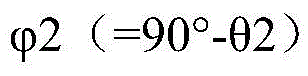 Enters the
 portion 23m of the emitting portion 23. Here, the magnitude relation of the reflection angles θ 0, θ 1, and θ 2 is reflected, and the angle of elevation is measured In the above-mentioned manner,
 the relationship of (1) holds. That is, the incident angle ι (see fig. 4) of the
 optical element 30 to the half mirror 31 is at an angle corresponding to the angle of elevation Corresponding portion
 23m, corresponding to elevation angle Corresponding portion
 23k, corresponding to elevation angle The order of the
 corresponding portions 23h becomes gradually smaller. In other words, the incident angle ι to the half mirror 31 or the reflection angle of the half mirror 31 becomes smaller as being away from the incident portion 21.
The overall behavior of the bundle of rays of the image light GL which is reflected by the plane 22a parallel to the outer periphery side of the light guide 22 and directed to the emitting portion 23 will be described.
As shown in fig. 3, in the cross section including the optical axis AX, the width of the light flux bundle of the image light GL is narrowed in any of the straight light paths P1 and P2 before and after being reflected by the region FR on the outer periphery side of the parallel light guide 22. Specifically, in the cross section including the optical axis AX, the beam of the image light GL is narrowed in width as a whole at a position crossing the straight light paths P1 and P2 in the vicinity of the region FR, that is, in the vicinity of the boundary between the straight light paths P1 and P2, and the beam width is narrowed. This makes it easy to make the angle of view in the lateral direction relatively large, because the bundle of rays of image light GL is narrowed in front of the emitting portion 23. In the illustrated example, the beam bundle of the image light GL is narrowed at a position crossing the straight light paths P1 and P2 to narrow the beam width, but may be narrowed only on one side of the straight light paths P1 and P2 to narrow the beam width.
(Structure of optical element)
Next, the structure of the optical element 30 constituting the emission portion 23 will be described.
Fig. 4 is an enlarged view of the optical element 30 of the present embodiment.
The emission portion 23 is constituted by an optical element 30, and the optical element 30 is provided parallel to the viewing side surface of the light guide 22. Therefore, the ejection portion 23 is provided along the XY plane inclined at the angle κ with respect to the optical axis AX, as in the parallel light guide 22.
As shown in fig. 4, the optical element 30 includes a plurality of half mirrors 31 and a plurality of light-transmitting members 32. The plurality of half mirrors 31 are disposed in parallel with each other with a space therebetween, reflect a part of the image light GL and the outside light EL, and transmit the other part of the image light GL and the outside light EL. The light-transmissive member 32 is interposed between two adjacent half mirrors 31 of the plurality of half mirrors 31. That is, the optical element 30 has the following structure: the half mirror 31 is interposed between each of the adjacent two translucent members 32 of the plurality of translucent members 32. In other words, the optical element 30 has a structure in which the half mirror 31 and the light-transmitting member 32 are alternately arranged.
The light-transmitting member 32 is a columnar member having a cross-sectional shape perpendicular to the longitudinal direction thereof in a parallelogram shape. Therefore, the translucent member 32 has two sets of a pair of planes extending parallel to the longitudinal direction and parallel to each other. Of the two sets of the pair of planes, one plane of the one set is an incident surface 32a on which the image light GL and the outside light EL are incident, and the other plane of the one set is an exit surface 32b from which the image light GL and the outside light EL exit. Further, a half mirror 31 is provided on one plane in the other group. The light-transmitting member 32 is made of, for example, glass, transparent resin, or the like.
The plurality of translucent members 32 are configured such that when a plurality of sets of a pair of translucent members 32 and half mirrors 31 are bonded together, the half mirrors 31 are arranged in parallel with each other. Although not shown in fig. 4, an adhesive layer is provided between one surface of the half mirror 31 and the adjacent translucent member 32. As a result, the optical element 30 is a rectangular plate-shaped member as a whole. When the optical element 30 is viewed in a direction normal to the incident surface 32a or the emission surface 32b of the light-transmissive member 32, the plurality of half mirrors 31 in a thin band shape are arranged in a band shape. That is, the optical element 30 has the following structure: a plurality of rectangular half mirrors 31 are arranged at a predetermined interval (pitch PT) in the X direction, which is a direction parallel to the direction in which the light guide 22 extends.
The half mirror 31 is formed of a reflective film sandwiched between light-transmissive members 32. The reflective film is composed of, for example, a dielectric multilayer film in which a plurality of dielectric thin films having different refractive indices are alternately stacked. Alternatively, the reflective film may be formed of a metal film. The half mirror 31 is provided such that the short side of the half mirror 31 is inclined with respect to the incident surface 32a and the exit surface 32b of the light-transmissive member 32. More specifically, the half mirror 31 is inclined toward the outside of the parallel light guide 22 so that the reflection surface faces the incident portion 21 side. In other words, the half mirror 31 is inclined in the following direction: the upper end (+ Z side) is rotated counterclockwise about the long side (Y direction) of the half mirror 31 as an axis and the YZ plane orthogonal to the planes 22a and 22b as a reference.
From the viewpoint of allowing the external light EL to pass through due to the perspective and facilitating the observation of the external image, the reflectance of the half mirror 31 with respect to the image light GL is, for example, 10% or more and 50% or less within a range of an assumed incident angle of the image light GL. Further, the half mirror 31 has a characteristic that the reflectance of the image light GL incident on the surface of the half mirror 31 at a relatively small incident angle is lower than the reflectance of the image light GL incident at a relatively large incident angle. The action and effect associated with this characteristic will be described in detail later.
Next, an angle formed by the reflection surface of the half mirror 31 and the emission surface 32b of the translucent member 32 is defined as an inclination angle δ of the half mirror 31. In the present embodiment, the inclination angle δ of the half mirror 31 is 45 ° or more and less than 90 °. In the present embodiment, the refractive index of the light-transmissive member 32 is equal to the refractive index of the parallel light guide 22, but these refractive indices may be different. When the refractive indexes are different, the inclination angle δ of the half mirror 31 needs to be changed as compared with the case where the refractive indexes are equal.
The half mirrors 31 are inclined clockwise at an angle δ of, for example, about 48 ° to 70 °, specifically, at an angle δ of, for example, 60 °, with respect to the viewer side surface 22b of the parallel light guide 22. Here, it is assumed that the image light GL0 has an angle of elevation For example, the angle of elevation of the image light GL1 is set to 30 DEG
 For example, the angle of elevation of the image light GL2 is set to 22 DEG
 For example, set to 38 °. In this case, as shown in fig. 3, the image light GL1 and the image light GL2 make an angle γ 1 ≈
 γ 2 ≈ 12.5 ° with respect to the optical axis AX, and enter the eye EY of the observer.
Accordingly, when a component having a relatively large total reflection angle in the image light GL (image light GL1) is mainly incident on the-x-side portion 23h side of the emitting unit 23 and a component having a relatively small total reflection angle (image light GL2) is mainly incident on the + x-side portion 23m side of the emitting unit 23, the image light GL can be efficiently extracted at an angle such that the entire image light GL converges on the eye EY of the observer. That is, the image light GL incident on the incident surface 32a of the optical element 30 from the parallel light guide 22 at a relatively large incident angle (relatively small elevation angle) can be efficiently extracted from the parallel light guide 22. Since the optical element 30 is configured to take out the image light GL at such an angle, the light guide device 20 can pass the image light GL only 1 time without passing the image light GL through the optical element 30 a plurality of times in principle. This allows image light GL to be extracted as virtual image light with less loss.
The pitch PT between adjacent half mirrors 31 is set to about 0.5mm to 2.0 mm. The pitch PT between the half mirrors 31 may not be strictly equally spaced, but may be arranged at a variable pitch. More specifically, the pitch PT of the half mirror 31 in the optical element 30 may be a random pitch that randomly increases and decreases around the reference interval. By arranging the half mirrors 31 in the optical element 30 at random pitches in this way, the occurrence of diffraction unevenness and moire can be suppressed. Further, the pitch is not limited to the random pitch, and a predetermined pitch pattern including pitches that increase and decrease in a plurality of stages, for example, may be repeated.
The thickness TI of the half mirror 31, which is the thickness of the optical element 30 in the Z-axis direction, is set to about 0.7mm to 3.0 mm. The thickness of the parallel light guide 22 supporting the optical element 30 is, for example, about several mm to 10mm, preferably about 4mm to 6 mm. When the thickness of the parallel light guide 22 is sufficiently larger than the thickness of the optical element 30, the incident angle of the image light GL on the optical element 30 or the boundary surface IF is easily reduced, and the reflection by the half mirror 31 at a position where the image light GL cannot be taken into the eye EY is easily suppressed. On the other hand, when the thickness of the parallel light guide 22 is made relatively thin, it is easy to achieve weight reduction of the parallel light guide 22 or the light guide device 20.
Fig. 5 is a diagram for explaining the operation of the optical element 30.
The present inventors investigated the cause of the leakage of the image light GL in the display device using the conventional optical element by using the ray tracing simulation.
As shown in FIG. 5, assume in elevation And left and right image light GL incident on the
 optical element 30. The image recognized by the observer as virtual image light is reflected light GL1 indicated by a dotted arrow. However, of the image light GL incident on the half mirror 31, a certain amount of light passes through the half mirror 31 without being deflected to the viewer side. For example, when the reflectance of the half mirror 31 is 20%, the image light GL passes through 4 half mirrors 31 because (1-0.2)4About 40% of the image light GL incident to the half mirror 31 passes through the half mirror 31 because of 0.41.
Then, the image light GL transmitted through the half mirror 31 enters the output surface 32b at an incident angle β of about 60 °, and is totally reflected by the output surface 32b and then travels toward the half mirror 31. As indicated by an arrow GL3 in a one-dot chain line, light of about six (1 to 0.41 equal to 0.59) in the image light GL totally reflected by the output surface 32b is reflected by the half mirror 31 and then returns to the output surface 32b again. At this time, light at an angle larger than the critical angle of the emission surface 32b is totally reflected again on the emission surface 32 b. The light totally reflected on the emission surface 32b enters the half mirror 31 at a relatively large incident angle, is reflected by the half mirror 31, passes through the parallel light guide 22, and is emitted from the plane 22a in the direction opposite to the observer side. Due to this light GL4, the following problems arise: people other than the observer can observe the image, and the secrecy of the image is impaired.
Therefore, the present inventors considered that the above problem can be improved by reducing the light that is totally reflected on the emission surface 32b, reflected by the half mirror 31, and returned to the emission surface 32b again. The light totally reflected on the exit surface 32b and traveling toward the half mirror 31 enters the half mirror 31 at a relatively small incident angle α. Therefore, if the half mirror 31 having the incident angle dependency that makes the reflectance of the image light GL incident on the surface of the half mirror 31 at the relatively small incident angle α lower than the reflectance of the image light GL incident at the relatively large incident angle α is used, the above-described problem can be improved.
As the half mirror 31 of the example in the ray tracing simulation, a laminated film composed of 8 films of various inorganic materials and metal materials shown in [ table 1] was assumed. Further, as the half mirror of the comparative example, a laminated film composed of 8 films of various inorganic materials and metal materials shown in [ table 2] was assumed.
[ Table 1]
| # | Material | Film thickness [ nm ]] |
| 1 | SiO2 | 7.4 |
| 2 | ZrO2 | 15.7 |
| 3 | SiO2 | 89.5 |
| 4 | ZrO2 | 39.8 |
| 5 | Ag | 12.8 |
| 6 | TiO2 | 58.2 |
| 7 | Al2O3 | 90.9 |
| 8 | Nb2O5 | 6.8 |
[ Table 2]
| # | Material | Film thickness [ nm ]] |
| 1 | ZrO2 | 56.3 |
| 2 | Ag | 12.4 |
| 3 | SiO2 | 12.9 |
| 4 | TiO2 | 45.0 |
| 5 | ZrO2 | 15.8 |
| 6 | Al2O3 | 31.7 |
| 7 | Nb2O5 | 17.0 |
| 8 | Al2O3 | 56.9 |
Fig. 6 is a graph showing the incident angle dependency of the reflectance of the half mirror of the embodiment and the comparative example. The horizontal axis of the graph is the incident angle [ degree (deg) ] and the vertical axis is the reflectance [% ].
The reflectance is calculated for the S-polarized light component and the P-polarized light component.
The graph denoted by reference numeral JS represents the reflectance of the half mirror of the embodiment with respect to the S-polarized light component, and the graph denoted by reference numeral JP represents the reflectance of the half mirror of the embodiment with respect to the P-polarized light component. The graph denoted by reference symbol CS represents the reflectance of the half mirror of the comparative example with respect to the S-polarized light component, and the graph denoted by reference symbol CP represents the reflectance of the half mirror of the comparative example with respect to the P-polarized light component.
As shown in fig. 6, the reflectance for the S-polarized light component and the reflectance for the P-polarized light component in each of the half mirror of the example and the half mirror of the comparative example show substantially the same characteristics. The reflectance of the half mirror of the comparative example was approximately 20% in the range of the incident angle of 10 ° to 55 °, and showed a substantially constant value. The reflectances for the S-polarized light component of the comparative examples were 19.1%, 19.6%, 19.7%, 19.4% and the reflectances for the P-polarized light component of the comparative examples were 19.0%, 18.9%, 18.8%, 19.3%, 19.7%, 20.1% at the incident angles of 11 °, 17 °, 23 °, 43 °, 49 °, 55 °. That is, the half mirror of the comparative example hardly has the incident angle dependency of the reflectance. In contrast, the reflectance of the half mirror of the example was approximately 20% which was equivalent to that of the comparative example when the incident angle was 55 °, but the reflectance decreased as the incident angle decreased from 55 °, and decreased to approximately 10% when the incident angle was 10 °. The reflectance for the S-polarized light component of the examples was 10.1%, 10.7%, 11.6%, 16.1%, 18.0%, 20.3% and the reflectance for the P-polarized light component of the examples was 9.9%, 10.2%, 10.7%, 15.8%, 18.2%, 20.5% at the incident angles of 11 °, 17 °, 23 °, 43 °, 49 °, 55 °.
By changing the material (stacking order) and/or the film thickness of the stacked film constituting the half mirror 31 in this way, the incident angle dependency of the reflectance of the half mirror 31 can be adjusted, and the half mirror 31 having a characteristic (incident angle dependency) in which the reflectance of light incident at a relatively small incident angle α is lower than the reflectance of light incident at a relatively large incident angle α can be realized.
Fig. 7 is a graph showing the luminance distribution of the back surface images formed by the optical elements of the examples and comparative examples. The back image is an image generated by light leaking from a plane 22a (back surface) of the parallel light guide 22 on the opposite side of the optical element 30. The horizontal axis of the graph represents the angle of view [ degree (deg) ], and the vertical axis represents the luminance [ nit (nit) ]. The angle of view is an angle corresponding to each position of the back surface image with respect to the optical axis AX (0 °).
The graph denoted by reference numeral J shows the luminance distribution of the back image in the display device using the half mirror of the embodiment, and the graph denoted by reference numeral C shows the luminance distribution of the back image in the display device using the half mirror of the comparative example.
As a result of simulation under the condition that the luminance of the image on the viewer side is 405nit, the luminance of the back surface image shifts around approximately 20 to 30nit in the display device having the half mirror of the comparative example. In contrast, in the display device 100 including the half mirror 31 of the embodiment, the luminance of the back image shifts around approximately 10 to 15 nit. As described above, it is understood that the display device 100 including the half mirror 31 of the embodiment can approximately halve the brightness of the back surface image as compared with the display device including the half mirror of the comparative example.
As described above, the optical element 30 of the present embodiment has the half mirror 31, and the half mirror 31 has a characteristic that the reflectance of light incident at the relatively small incident angle α is lower than the reflectance of light incident at the relatively large incident angle α, so that it is possible to reduce the leakage of image light from the plane 22a side of the parallel light guide 22. As a result, according to the present embodiment, the following display device 100 can be realized: it is difficult for people other than the observer to visually recognize the image, and the concealing property of the image is excellent.
In the display device 100 of the present embodiment, the light-emitting portion 23 is provided parallel to the viewing-side plane 22b of the light guide 22, and therefore the image light GL emitted from the optical element 30 reaches the eyes of the observer without being incident on other members. Therefore, the display device 100 with easy optical design can be realized.
The technical scope of the present invention is not limited to the above-described embodiments, and various modifications can be made without departing from the scope of the present invention.
For example, in the above-described embodiment, the half mirrors having the same incident angle dependency of reflectance are used in the range of all the half mirrors constituting the optical element, but for example, a plurality of kinds of half mirrors having different incident angle dependencies of reflectance depending on the position of the optical element may be used instead of this configuration.
In addition, the specific configuration of each part such as the number, shape, and material of each component constituting the optical element and the display device is not limited to the above embodiment, and can be appropriately modified. For example, as the image forming apparatus, in addition to the organic EL element, a combination of a liquid crystal display element, a laser light source, and a MEMS (Micro-Electro-Mechanical System) scanner may be used.
Claims (4)
1. An optical element, comprising:
a plurality of half mirrors which are disposed in parallel with each other with a space therebetween and reflect a part of image light and external light and transmit the other part of the image light and the external light; and
a light-transmissive member interposed between adjacent two of the half mirrors among the plurality of half mirrors,
the light-transmitting member includes: an incident surface to which the image light and the external light are incident via a light guide; and an emission surface that emits the image and the external light to a viewer side,
the plurality of half mirrors are each arranged to be inclined with respect to the incident surface and the exit surface, respectively, and the reflectance of light incident on the surface of each half mirror at a relatively small incident angle is lower than the reflectance of light incident at a relatively large incident angle,
the plurality of half mirrors respectively include dielectric multilayer films.
2. The optical element according to claim 1,
an angle formed by each of the half mirrors and the emission surface is 45 ° or more and less than 90 °.
3. A display device is characterized by comprising:
an image forming apparatus; and
a light guide device that guides the image light generated by the image forming device,
the light guide device has: an incident portion to which the image light is incident; a light guide that guides the image light incident from the incident portion; and an emission unit that emits the image light,
the emission part has the optical element according to claim 1 or 2.
4. The display device according to claim 3,
the emission portion is provided on a surface of the light guide body on the viewing side.
Applications Claiming Priority (4)
| Application Number | Priority Date | Filing Date | Title |
|---|---|---|---|
| JP2016-186606 | 2016-09-26 | ||
| JP2016186606 | 2016-09-26 | ||
| JP2017-138794 | 2017-07-18 | ||
| JP2017138794A JP2018055085A (en) | 2016-09-26 | 2017-07-18 | Optical element and display device |
Publications (2)
| Publication Number | Publication Date |
|---|---|
| CN107870430A CN107870430A (en) | 2018-04-03 |
| CN107870430B true CN107870430B (en) | 2021-06-15 |
Family
ID=61685260
Family Applications (1)
| Application Number | Title | Priority Date | Filing Date |
|---|---|---|---|
| CN201710822152.3A Active CN107870430B (en) | 2016-09-26 | 2017-09-13 | Optical Components and Display Devices |
Country Status (2)
| Country | Link |
|---|---|
| US (1) | US10295829B2 (en) |
| CN (1) | CN107870430B (en) |
Families Citing this family (4)
| Publication number | Priority date | Publication date | Assignee | Title |
|---|---|---|---|---|
| TWI813691B (en) | 2018-05-23 | 2023-09-01 | 以色列商魯姆斯有限公司 | Optical system including light-guide optical element with partially-reflective internal surfaces |
| CN109199332B (en) * | 2018-09-28 | 2021-12-07 | 同济大学 | Photoacoustic and ultrasonic bimodal endoscopic imaging device and method based on light reflection |
| JP7407368B2 (en) * | 2020-03-30 | 2024-01-04 | パナソニックIpマネジメント株式会社 | display device |
| CN115685552A (en) * | 2021-07-30 | 2023-02-03 | 株式会社理光 | Light guide member and virtual image display device |
Citations (4)
| Publication number | Priority date | Publication date | Assignee | Title |
|---|---|---|---|---|
| EP0399865A1 (en) * | 1989-05-23 | 1990-11-28 | Thomson-Csf | Optical device for introduction of a collimated image into the field of view of an observer and helmet comprising such a device |
| CN104570352A (en) * | 2015-01-06 | 2015-04-29 | 华为技术有限公司 | Near-eye display |
| WO2016027442A1 (en) * | 2014-08-18 | 2016-02-25 | Seiko Epson Corporation | Light guide device and virtual image display apparatus |
| US9274338B2 (en) * | 2012-03-21 | 2016-03-01 | Microsoft Technology Licensing, Llc | Increasing field of view of reflective waveguide |
Family Cites Families (11)
| Publication number | Priority date | Publication date | Assignee | Title |
|---|---|---|---|---|
| WO2001095027A2 (en) | 2000-06-05 | 2001-12-13 | Lumus Ltd. | Substrate-guided optical beam expander |
| IL148804A (en) | 2002-03-21 | 2007-02-11 | Yaacov Amitai | Optical device |
| IL157837A (en) | 2003-09-10 | 2012-12-31 | Yaakov Amitai | Substrate-guided optical device particularly for three-dimensional displays |
| EP2243051A1 (en) * | 2007-12-18 | 2010-10-27 | BAE Systems PLC | Improvemements in or relating to display projectors |
| US8917453B2 (en) | 2011-12-23 | 2014-12-23 | Microsoft Corporation | Reflective array waveguide |
| US8989535B2 (en) * | 2012-06-04 | 2015-03-24 | Microsoft Technology Licensing, Llc | Multiple waveguide imaging structure |
| US9946069B2 (en) * | 2013-03-28 | 2018-04-17 | Bae Systems Plc | Displays |
| JP6201836B2 (en) * | 2014-03-14 | 2017-09-27 | ソニー株式会社 | Optical device and method for assembling the same, hologram diffraction grating, display device and alignment device |
| JP2016085430A (en) * | 2014-10-29 | 2016-05-19 | セイコーエプソン株式会社 | Virtual image display device |
| US10670862B2 (en) * | 2015-07-02 | 2020-06-02 | Microsoft Technology Licensing, Llc | Diffractive optical elements with asymmetric profiles |
| US9864208B2 (en) * | 2015-07-30 | 2018-01-09 | Microsoft Technology Licensing, Llc | Diffractive optical elements with varying direction for depth modulation |
-
2017
- 2017-09-13 CN CN201710822152.3A patent/CN107870430B/en active Active
- 2017-09-13 US US15/703,152 patent/US10295829B2/en active Active
Patent Citations (4)
| Publication number | Priority date | Publication date | Assignee | Title |
|---|---|---|---|---|
| EP0399865A1 (en) * | 1989-05-23 | 1990-11-28 | Thomson-Csf | Optical device for introduction of a collimated image into the field of view of an observer and helmet comprising such a device |
| US9274338B2 (en) * | 2012-03-21 | 2016-03-01 | Microsoft Technology Licensing, Llc | Increasing field of view of reflective waveguide |
| WO2016027442A1 (en) * | 2014-08-18 | 2016-02-25 | Seiko Epson Corporation | Light guide device and virtual image display apparatus |
| CN104570352A (en) * | 2015-01-06 | 2015-04-29 | 华为技术有限公司 | Near-eye display |
Also Published As
| Publication number | Publication date |
|---|---|
| US10295829B2 (en) | 2019-05-21 |
| US20180088337A1 (en) | 2018-03-29 |
| CN107870430A (en) | 2018-04-03 |
Similar Documents
| Publication | Publication Date | Title |
|---|---|---|
| JP5459150B2 (en) | Light guide plate and virtual image display device including the same | |
| CN108663810B (en) | Light guide device and display device | |
| CN107167919B (en) | Light guide device and virtual image display device | |
| JP6409401B2 (en) | Light guide device and virtual image display device | |
| CN108254918B (en) | Optical element and display device | |
| CN107238926B (en) | Optical element, display device, and manufacturing method of optical element | |
| CN107861243B (en) | Optical Components and Display Devices | |
| TW201608282A (en) | Light guide device and virtual image display apparatus | |
| JP5408048B2 (en) | Light guide plate for virtual image display device and virtual image display device | |
| CN109946839A (en) | display device | |
| CN107870430B (en) | Optical Components and Display Devices | |
| JP2012123147A (en) | Light guide plate, method for manufacturing light guide plate and virtual image display device | |
| JP2017003845A (en) | Light guide device and virtual image display device | |
| CN115004080B (en) | Light guide and virtual image display device | |
| JP2018109738A (en) | Optical element and display device | |
| JP2017049511A (en) | Light guide device and virtual image display device | |
| JP2018106104A (en) | Display unit | |
| CN107870426B (en) | Optical Components and Display Devices | |
| JP2017161564A (en) | Light guide device and virtual image display device | |
| JP2019197079A (en) | Virtual image display device | |
| JP2018055085A (en) | Optical element and display device | |
| JP2012098324A (en) | Light guide plate and virtual image display device having the same | |
| JP2026004785A (en) | Virtual image display device and optical unit | |
| JP6436221B2 (en) | Virtual image display device | |
| JP2017161563A (en) | Light guide device and virtual image display device |
Legal Events
| Date | Code | Title | Description |
|---|---|---|---|
| PB01 | Publication | ||
| PB01 | Publication | ||
| SE01 | Entry into force of request for substantive examination | ||
| SE01 | Entry into force of request for substantive examination | ||
| GR01 | Patent grant | ||
| GR01 | Patent grant |