CN107851712B - Polish stop layer for processing semiconductor element arrays - Google Patents
Polish stop layer for processing semiconductor element arrays Download PDFInfo
- Publication number
- CN107851712B CN107851712B CN201680044692.7A CN201680044692A CN107851712B CN 107851712 B CN107851712 B CN 107851712B CN 201680044692 A CN201680044692 A CN 201680044692A CN 107851712 B CN107851712 B CN 107851712B
- Authority
- CN
- China
- Prior art keywords
- layer
- mtj
- cmp
- top surface
- pillars
- Prior art date
- Legal status (The legal status is an assumption and is not a legal conclusion. Google has not performed a legal analysis and makes no representation as to the accuracy of the status listed.)
- Active
Links
Images


Classifications
-
- H—ELECTRICITY
- H10—SEMICONDUCTOR DEVICES; ELECTRIC SOLID-STATE DEVICES NOT OTHERWISE PROVIDED FOR
- H10N—ELECTRIC SOLID-STATE DEVICES NOT OTHERWISE PROVIDED FOR
- H10N50/00—Galvanomagnetic devices
- H10N50/01—Manufacture or treatment
-
- H—ELECTRICITY
- H10—SEMICONDUCTOR DEVICES; ELECTRIC SOLID-STATE DEVICES NOT OTHERWISE PROVIDED FOR
- H10B—ELECTRONIC MEMORY DEVICES
- H10B61/00—Magnetic memory devices, e.g. magnetoresistive RAM [MRAM] devices
-
- H—ELECTRICITY
- H10—SEMICONDUCTOR DEVICES; ELECTRIC SOLID-STATE DEVICES NOT OTHERWISE PROVIDED FOR
- H10N—ELECTRIC SOLID-STATE DEVICES NOT OTHERWISE PROVIDED FOR
- H10N50/00—Galvanomagnetic devices
- H10N50/10—Magnetoresistive devices
-
- H—ELECTRICITY
- H10—SEMICONDUCTOR DEVICES; ELECTRIC SOLID-STATE DEVICES NOT OTHERWISE PROVIDED FOR
- H10N—ELECTRIC SOLID-STATE DEVICES NOT OTHERWISE PROVIDED FOR
- H10N50/00—Galvanomagnetic devices
- H10N50/80—Constructional details
-
- H10P52/00—
Landscapes
- Engineering & Computer Science (AREA)
- Manufacturing & Machinery (AREA)
- Hall/Mr Elements (AREA)
- Mram Or Spin Memory Techniques (AREA)
- Mechanical Treatment Of Semiconductor (AREA)
- Physics & Mathematics (AREA)
- Condensed Matter Physics & Semiconductors (AREA)
- General Physics & Mathematics (AREA)
- Computer Hardware Design (AREA)
- Microelectronics & Electronic Packaging (AREA)
- Power Engineering (AREA)
- Semiconductor Memories (AREA)
Abstract
所描述的实施例可用于半导体制造中且采用具有高和低抛光速率的材料来帮助确定在整个晶片中一致且可在损坏半导体元件之前停止抛光的精确抛光终点。使用所述半导体元件之间的所述低抛光速率材料的高度作为所述抛光终点。由于所述低抛光速率材料减缓抛光工艺,因此容易确定终点且避免损坏所述半导体元件。另一或替代蚀刻终点可为薄材料层,其在暴露时提供极清晰的光谱信号,从而容许所述蚀刻工艺停止。
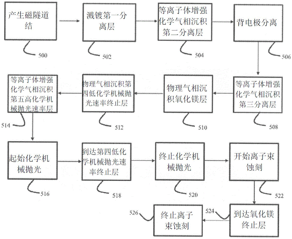
The described embodiments can be used in semiconductor fabrication and employ materials with high and low polishing rates to help determine precise polishing endpoints that are consistent throughout a wafer and that can stop polishing before damaging semiconductor elements. The height of the low polishing rate material between the semiconductor elements is used as the polishing endpoint. Since the low polishing rate material slows down the polishing process, endpoints are easily determined and damage to the semiconductor element is avoided. Another or alternative etch endpoint may be a thin layer of material that provides a very clear spectral signal upon exposure, allowing the etch process to stop.
Description
Claims (26)
Applications Claiming Priority (5)
| Application Number | Priority Date | Filing Date | Title |
|---|---|---|---|
| US201562198870P | 2015-07-30 | 2015-07-30 | |
| US62/198,870 | 2015-07-30 | ||
| US15/097,576 US9773974B2 (en) | 2015-07-30 | 2016-04-13 | Polishing stop layer(s) for processing arrays of semiconductor elements |
| US15/097,576 | 2016-04-13 | ||
| PCT/US2016/027445 WO2017019134A1 (en) | 2015-07-30 | 2016-04-14 | Polishing stop layer(s) for processing arrays of semiconductor elements |
Publications (2)
| Publication Number | Publication Date |
|---|---|
| CN107851712A CN107851712A (en) | 2018-03-27 |
| CN107851712B true CN107851712B (en) | 2021-10-29 |
Family
ID=57883324
Family Applications (1)
| Application Number | Title | Priority Date | Filing Date |
|---|---|---|---|
| CN201680044692.7A Active CN107851712B (en) | 2015-07-30 | 2016-04-14 | Polish stop layer for processing semiconductor element arrays |
Country Status (5)
| Country | Link |
|---|---|
| US (2) | US9773974B2 (en) |
| JP (1) | JP2018527747A (en) |
| KR (1) | KR102500584B1 (en) |
| CN (1) | CN107851712B (en) |
| WO (1) | WO2017019134A1 (en) |
Families Citing this family (74)
| Publication number | Priority date | Publication date | Assignee | Title |
|---|---|---|---|---|
| US10468590B2 (en) | 2015-04-21 | 2019-11-05 | Spin Memory, Inc. | High annealing temperature perpendicular magnetic anisotropy structure for magnetic random access memory |
| US9728712B2 (en) | 2015-04-21 | 2017-08-08 | Spin Transfer Technologies, Inc. | Spin transfer torque structure for MRAM devices having a spin current injection capping layer |
| US9853206B2 (en) | 2015-06-16 | 2017-12-26 | Spin Transfer Technologies, Inc. | Precessional spin current structure for MRAM |
| US9773974B2 (en) | 2015-07-30 | 2017-09-26 | Spin Transfer Technologies, Inc. | Polishing stop layer(s) for processing arrays of semiconductor elements |
| US10163479B2 (en) | 2015-08-14 | 2018-12-25 | Spin Transfer Technologies, Inc. | Method and apparatus for bipolar memory write-verify |
| US9741926B1 (en) | 2016-01-28 | 2017-08-22 | Spin Transfer Technologies, Inc. | Memory cell having magnetic tunnel junction and thermal stability enhancement layer |
| US10818331B2 (en) | 2016-09-27 | 2020-10-27 | Spin Memory, Inc. | Multi-chip module for MRAM devices with levels of dynamic redundancy registers |
| US10546625B2 (en) | 2016-09-27 | 2020-01-28 | Spin Memory, Inc. | Method of optimizing write voltage based on error buffer occupancy |
| US10360964B2 (en) | 2016-09-27 | 2019-07-23 | Spin Memory, Inc. | Method of writing contents in memory during a power up sequence using a dynamic redundancy register in a memory device |
| US10366774B2 (en) | 2016-09-27 | 2019-07-30 | Spin Memory, Inc. | Device with dynamic redundancy registers |
| US10437723B2 (en) | 2016-09-27 | 2019-10-08 | Spin Memory, Inc. | Method of flushing the contents of a dynamic redundancy register to a secure storage area during a power down in a memory device |
| US10991410B2 (en) | 2016-09-27 | 2021-04-27 | Spin Memory, Inc. | Bi-polar write scheme |
| US10460781B2 (en) | 2016-09-27 | 2019-10-29 | Spin Memory, Inc. | Memory device with a dual Y-multiplexer structure for performing two simultaneous operations on the same row of a memory bank |
| US10446210B2 (en) | 2016-09-27 | 2019-10-15 | Spin Memory, Inc. | Memory instruction pipeline with a pre-read stage for a write operation for reducing power consumption in a memory device that uses dynamic redundancy registers |
| US10437491B2 (en) | 2016-09-27 | 2019-10-08 | Spin Memory, Inc. | Method of processing incomplete memory operations in a memory device during a power up sequence and a power down sequence using a dynamic redundancy register |
| US10665777B2 (en) | 2017-02-28 | 2020-05-26 | Spin Memory, Inc. | Precessional spin current structure with non-magnetic insertion layer for MRAM |
| US10672976B2 (en) | 2017-02-28 | 2020-06-02 | Spin Memory, Inc. | Precessional spin current structure with high in-plane magnetization for MRAM |
| US10032978B1 (en) | 2017-06-27 | 2018-07-24 | Spin Transfer Technologies, Inc. | MRAM with reduced stray magnetic fields |
| US10656994B2 (en) | 2017-10-24 | 2020-05-19 | Spin Memory, Inc. | Over-voltage write operation of tunnel magnet-resistance (“TMR”) memory device and correcting failure bits therefrom by using on-the-fly bit failure detection and bit redundancy remapping techniques |
| US10529439B2 (en) | 2017-10-24 | 2020-01-07 | Spin Memory, Inc. | On-the-fly bit failure detection and bit redundancy remapping techniques to correct for fixed bit defects |
| US10489245B2 (en) | 2017-10-24 | 2019-11-26 | Spin Memory, Inc. | Forcing stuck bits, waterfall bits, shunt bits and low TMR bits to short during testing and using on-the-fly bit failure detection and bit redundancy remapping techniques to correct them |
| US10481976B2 (en) | 2017-10-24 | 2019-11-19 | Spin Memory, Inc. | Forcing bits as bad to widen the window between the distributions of acceptable high and low resistive bits thereby lowering the margin and increasing the speed of the sense amplifiers |
| WO2019116654A1 (en) * | 2017-12-13 | 2019-06-20 | ソニー株式会社 | Method for manufacturing light-emitting module, light-emitting module, and device |
| US10424726B2 (en) | 2017-12-28 | 2019-09-24 | Spin Memory, Inc. | Process for improving photoresist pillar adhesion during MRAM fabrication |
| US10395711B2 (en) | 2017-12-28 | 2019-08-27 | Spin Memory, Inc. | Perpendicular source and bit lines for an MRAM array |
| US10360962B1 (en) | 2017-12-28 | 2019-07-23 | Spin Memory, Inc. | Memory array with individually trimmable sense amplifiers |
| US10395712B2 (en) | 2017-12-28 | 2019-08-27 | Spin Memory, Inc. | Memory array with horizontal source line and sacrificial bitline per virtual source |
| US10891997B2 (en) | 2017-12-28 | 2021-01-12 | Spin Memory, Inc. | Memory array with horizontal source line and a virtual source line |
| US10811594B2 (en) | 2017-12-28 | 2020-10-20 | Spin Memory, Inc. | Process for hard mask development for MRAM pillar formation using photolithography |
| US10840439B2 (en) | 2017-12-29 | 2020-11-17 | Spin Memory, Inc. | Magnetic tunnel junction (MTJ) fabrication methods and systems |
| US10270027B1 (en) | 2017-12-29 | 2019-04-23 | Spin Memory, Inc. | Self-generating AC current assist in orthogonal STT-MRAM |
| US10784439B2 (en) | 2017-12-29 | 2020-09-22 | Spin Memory, Inc. | Precessional spin current magnetic tunnel junction devices and methods of manufacture |
| US10424723B2 (en) | 2017-12-29 | 2019-09-24 | Spin Memory, Inc. | Magnetic tunnel junction devices including an optimization layer |
| US10236047B1 (en) | 2017-12-29 | 2019-03-19 | Spin Memory, Inc. | Shared oscillator (STNO) for MRAM array write-assist in orthogonal STT-MRAM |
| US10840436B2 (en) | 2017-12-29 | 2020-11-17 | Spin Memory, Inc. | Perpendicular magnetic anisotropy interface tunnel junction devices and methods of manufacture |
| US10367139B2 (en) | 2017-12-29 | 2019-07-30 | Spin Memory, Inc. | Methods of manufacturing magnetic tunnel junction devices |
| US10199083B1 (en) | 2017-12-29 | 2019-02-05 | Spin Transfer Technologies, Inc. | Three-terminal MRAM with ac write-assist for low read disturb |
| US10236048B1 (en) | 2017-12-29 | 2019-03-19 | Spin Memory, Inc. | AC current write-assist in orthogonal STT-MRAM |
| US10360961B1 (en) | 2017-12-29 | 2019-07-23 | Spin Memory, Inc. | AC current pre-charge write-assist in orthogonal STT-MRAM |
| US10886330B2 (en) | 2017-12-29 | 2021-01-05 | Spin Memory, Inc. | Memory device having overlapping magnetic tunnel junctions in compliance with a reference pitch |
| US10546624B2 (en) | 2017-12-29 | 2020-01-28 | Spin Memory, Inc. | Multi-port random access memory |
| US10339993B1 (en) | 2017-12-30 | 2019-07-02 | Spin Memory, Inc. | Perpendicular magnetic tunnel junction device with skyrmionic assist layers for free layer switching |
| US10319900B1 (en) | 2017-12-30 | 2019-06-11 | Spin Memory, Inc. | Perpendicular magnetic tunnel junction device with precessional spin current layer having a modulated moment density |
| US10229724B1 (en) | 2017-12-30 | 2019-03-12 | Spin Memory, Inc. | Microwave write-assist in series-interconnected orthogonal STT-MRAM devices |
| US10141499B1 (en) | 2017-12-30 | 2018-11-27 | Spin Transfer Technologies, Inc. | Perpendicular magnetic tunnel junction device with offset precessional spin current layer |
| US10255962B1 (en) | 2017-12-30 | 2019-04-09 | Spin Memory, Inc. | Microwave write-assist in orthogonal STT-MRAM |
| US10236439B1 (en) | 2017-12-30 | 2019-03-19 | Spin Memory, Inc. | Switching and stability control for perpendicular magnetic tunnel junction device |
| US10468588B2 (en) | 2018-01-05 | 2019-11-05 | Spin Memory, Inc. | Perpendicular magnetic tunnel junction device with skyrmionic enhancement layers for the precessional spin current magnetic layer |
| US10438995B2 (en) | 2018-01-08 | 2019-10-08 | Spin Memory, Inc. | Devices including magnetic tunnel junctions integrated with selectors |
| US10438996B2 (en) | 2018-01-08 | 2019-10-08 | Spin Memory, Inc. | Methods of fabricating magnetic tunnel junctions integrated with selectors |
| US10446744B2 (en) | 2018-03-08 | 2019-10-15 | Spin Memory, Inc. | Magnetic tunnel junction wafer adaptor used in magnetic annealing furnace and method of using the same |
| US11107978B2 (en) | 2018-03-23 | 2021-08-31 | Spin Memory, Inc. | Methods of manufacturing three-dimensional arrays with MTJ devices including a free magnetic trench layer and a planar reference magnetic layer |
| US10784437B2 (en) | 2018-03-23 | 2020-09-22 | Spin Memory, Inc. | Three-dimensional arrays with MTJ devices including a free magnetic trench layer and a planar reference magnetic layer |
| US10734573B2 (en) | 2018-03-23 | 2020-08-04 | Spin Memory, Inc. | Three-dimensional arrays with magnetic tunnel junction devices including an annular discontinued free magnetic layer and a planar reference magnetic layer |
| US11107974B2 (en) | 2018-03-23 | 2021-08-31 | Spin Memory, Inc. | Magnetic tunnel junction devices including a free magnetic trench layer and a planar reference magnetic layer |
| US10411185B1 (en) | 2018-05-30 | 2019-09-10 | Spin Memory, Inc. | Process for creating a high density magnetic tunnel junction array test platform |
| US10680169B2 (en) | 2018-06-13 | 2020-06-09 | International Business Machines Corporation | Multilayer hardmask for high performance MRAM devices |
| US10559338B2 (en) | 2018-07-06 | 2020-02-11 | Spin Memory, Inc. | Multi-bit cell read-out techniques |
| US10692569B2 (en) | 2018-07-06 | 2020-06-23 | Spin Memory, Inc. | Read-out techniques for multi-bit cells |
| US10600478B2 (en) | 2018-07-06 | 2020-03-24 | Spin Memory, Inc. | Multi-bit cell read-out techniques for MRAM cells with mixed pinned magnetization orientations |
| US10593396B2 (en) | 2018-07-06 | 2020-03-17 | Spin Memory, Inc. | Multi-bit cell read-out techniques for MRAM cells with mixed pinned magnetization orientations |
| US10650875B2 (en) | 2018-08-21 | 2020-05-12 | Spin Memory, Inc. | System for a wide temperature range nonvolatile memory |
| US10699761B2 (en) | 2018-09-18 | 2020-06-30 | Spin Memory, Inc. | Word line decoder memory architecture |
| US10971680B2 (en) | 2018-10-01 | 2021-04-06 | Spin Memory, Inc. | Multi terminal device stack formation methods |
| US11621293B2 (en) | 2018-10-01 | 2023-04-04 | Integrated Silicon Solution, (Cayman) Inc. | Multi terminal device stack systems and methods |
| US10714681B2 (en) | 2018-10-19 | 2020-07-14 | International Business Machines Corporation | Embedded magnetic tunnel junction pillar having reduced height and uniform contact area |
| US10672611B2 (en) | 2018-10-19 | 2020-06-02 | International Business Machines Corporation | Hardmask stress, grain, and structure engineering for advanced memory applications |
| CN111162164B (en) * | 2018-11-08 | 2023-06-13 | 江苏鲁汶仪器股份有限公司 | Manufacturing method of semiconductor device |
| US10580827B1 (en) | 2018-11-16 | 2020-03-03 | Spin Memory, Inc. | Adjustable stabilizer/polarizer method for MRAM with enhanced stability and efficient switching |
| US11031250B2 (en) | 2018-11-29 | 2021-06-08 | International Business Machines Corporation | Semiconductor structures of more uniform thickness |
| US11107979B2 (en) | 2018-12-28 | 2021-08-31 | Spin Memory, Inc. | Patterned silicide structures and methods of manufacture |
| CN111816764B (en) * | 2019-04-11 | 2024-05-28 | 上海磁宇信息科技有限公司 | Method for preparing magnetic tunnel junction cell array |
| US11187764B2 (en) * | 2020-03-20 | 2021-11-30 | Allegro Microsystems, Llc | Layout of magnetoresistance element |
| US12248039B2 (en) | 2023-08-08 | 2025-03-11 | Allegro Microsystems, Llc | Interleaving sub-arrays of magnetoresistance elements based on reference directions to compensate for bridge offset |
Citations (3)
| Publication number | Priority date | Publication date | Assignee | Title |
|---|---|---|---|---|
| CN101976723A (en) * | 2010-08-10 | 2011-02-16 | 杭州电子科技大学 | Manufacture method of current isolator |
| CN102339734A (en) * | 2010-07-15 | 2012-02-01 | 中芯国际集成电路制造(上海)有限公司 | Production method of cylindrical semiconductor device with cross section being circular ring |
| CN102479920A (en) * | 2010-11-30 | 2012-05-30 | 中芯国际集成电路制造(上海)有限公司 | Manufacture method of nanometer annular magnetic tunnel structure and manufacture method of magnetic resistance internal memory |
Family Cites Families (305)
| Publication number | Priority date | Publication date | Assignee | Title |
|---|---|---|---|---|
| US341801A (en) | 1886-05-11 | Appaeatus foe peepaeing geain foe mashing | ||
| US5597437A (en) | 1995-01-12 | 1997-01-28 | Procter & Gamble | Zero scrap absorbent core formation process |
| US5541868A (en) | 1995-02-21 | 1996-07-30 | The United States Of America As Represented By The Secretary Of The Navy | Annular GMR-based memory element |
| US5654566A (en) | 1995-04-21 | 1997-08-05 | Johnson; Mark B. | Magnetic spin injected field effect transistor and method of operation |
| US6140838A (en) | 1995-04-21 | 2000-10-31 | Johnson; Mark B. | High density and high speed magneto-electronic logic family |
| US5629549A (en) | 1995-04-21 | 1997-05-13 | Johnson; Mark B. | Magnetic spin transistor device, logic gate & method of operation |
| US5896252A (en) | 1995-08-11 | 1999-04-20 | Fujitsu Limited | Multilayer spin valve magneto-resistive effect magnetic head with free magnetic layer including two sublayers and magnetic disk drive including same |
| JP3207094B2 (en) | 1995-08-21 | 2001-09-10 | 松下電器産業株式会社 | Magnetoresistance effect element and memory element |
| US5695864A (en) | 1995-09-28 | 1997-12-09 | International Business Machines Corporation | Electronic device using magnetic components |
| FR2743930B1 (en) | 1996-01-19 | 2000-04-07 | Fujitsu Ltd | MAGNETIC SENSOR FOR READING RECORDING MEDIA |
| US5640343A (en) | 1996-03-18 | 1997-06-17 | International Business Machines Corporation | Magnetic memory array using magnetic tunnel junction devices in the memory cells |
| JP3327375B2 (en) | 1996-04-26 | 2002-09-24 | 富士通株式会社 | Magnetoresistive transducer, method of manufacturing the same, and magnetic recording apparatus |
| JP3447468B2 (en) | 1996-06-17 | 2003-09-16 | シャープ株式会社 | Magnetoresistive element, method of manufacturing the same, and magnetic head using the same |
| US5732016A (en) | 1996-07-02 | 1998-03-24 | Motorola | Memory cell structure in a magnetic random access memory and a method for fabricating thereof |
| US5768069A (en) | 1996-11-27 | 1998-06-16 | International Business Machines Corporation | Self-biased dual spin valve sensor |
| JP3557078B2 (en) | 1997-06-27 | 2004-08-25 | 株式会社東芝 | Nonvolatile semiconductor memory device |
| JP4066477B2 (en) | 1997-10-09 | 2008-03-26 | ソニー株式会社 | Nonvolatile random access memory device |
| US5966323A (en) | 1997-12-18 | 1999-10-12 | Motorola, Inc. | Low switching field magnetoresistive tunneling junction for high density arrays |
| US6055179A (en) | 1998-05-19 | 2000-04-25 | Canon Kk | Memory device utilizing giant magnetoresistance effect |
| JPH11352867A (en) | 1998-06-05 | 1999-12-24 | Nippon Telegr & Teleph Corp <Ntt> | Server-client type learning support system, method, and recording medium storing learning support program |
| US6130814A (en) | 1998-07-28 | 2000-10-10 | International Business Machines Corporation | Current-induced magnetic switching device and memory including the same |
| US6172902B1 (en) | 1998-08-12 | 2001-01-09 | Ecole Polytechnique Federale De Lausanne (Epfl) | Non-volatile magnetic random access memory |
| US6097579A (en) | 1998-08-21 | 2000-08-01 | International Business Machines Corporation | Tunnel junction head structure without current shunting |
| US6016269A (en) | 1998-09-30 | 2000-01-18 | Motorola, Inc. | Quantum random address memory with magnetic readout and/or nano-memory elements |
| JP3766565B2 (en) | 1999-05-31 | 2006-04-12 | Tdk株式会社 | Magnetoresistive film and magnetoresistive head |
| US6436526B1 (en) | 1999-06-17 | 2002-08-20 | Matsushita Electric Industrial Co., Ltd. | Magneto-resistance effect element, magneto-resistance effect memory cell, MRAM and method for performing information write to or read from the magneto-resistance effect memory cell |
| WO2001001396A1 (en) | 1999-06-29 | 2001-01-04 | Fujitsu Limited | Magnetoresistive head and device for information reproduction |
| US6292389B1 (en) | 1999-07-19 | 2001-09-18 | Motorola, Inc. | Magnetic element with improved field response and fabricating method thereof |
| US6134138A (en) | 1999-07-30 | 2000-10-17 | Honeywell Inc. | Method and apparatus for reading a magnetoresistive memory |
| JP3793669B2 (en) | 1999-08-26 | 2006-07-05 | 株式会社日立グローバルストレージテクノロジーズ | Giant magnetoresistive head, thin film magnetic head, and magnetic recording / reproducing apparatus |
| US6611405B1 (en) | 1999-09-16 | 2003-08-26 | Kabushiki Kaisha Toshiba | Magnetoresistive element and magnetic memory device |
| KR100373473B1 (en) | 1999-09-24 | 2003-02-25 | 가부시끼가이샤 도시바 | Magnetoresistance device, magnetoresistance head, magnetoreproducing device, and magnetic stacked body |
| JP3891540B2 (en) | 1999-10-25 | 2007-03-14 | キヤノン株式会社 | Magnetoresistive memory, method for recording / reproducing information recorded in magnetoresistive memory, and MRAM |
| US6447935B1 (en) | 1999-11-23 | 2002-09-10 | Read-Rite Corporation | Method and system for reducing assymetry in a spin valve having a synthetic pinned layer |
| US6233172B1 (en) | 1999-12-17 | 2001-05-15 | Motorola, Inc. | Magnetic element with dual magnetic states and fabrication method thereof |
| US6272036B1 (en) | 1999-12-20 | 2001-08-07 | The University Of Chicago | Control of magnetic direction in multi-layer ferromagnetic devices by bias voltage |
| TW504713B (en) | 2000-04-28 | 2002-10-01 | Motorola Inc | Magnetic element with insulating veils and fabricating method thereof |
| US6570139B1 (en) | 2000-04-28 | 2003-05-27 | The Holmes Group, Inc. | Electronic control circuit |
| US6522137B1 (en) | 2000-06-28 | 2003-02-18 | Schlumberger Technology Corporation | Two-dimensional magnetic resonance imaging in a borehole |
| JP2004502705A (en) | 2000-07-03 | 2004-01-29 | メルク エンド カムパニー インコーポレーテッド | Coding methods in combinatorial libraries |
| US6493259B1 (en) | 2000-08-14 | 2002-12-10 | Micron Technology, Inc. | Pulse write techniques for magneto-resistive memories |
| DE10050076C2 (en) | 2000-10-10 | 2003-09-18 | Infineon Technologies Ag | Method for producing a ferromagnetic structure and ferromagnetic component |
| US6385082B1 (en) | 2000-11-08 | 2002-05-07 | International Business Machines Corp. | Thermally-assisted magnetic random access memory (MRAM) |
| FR2817999B1 (en) | 2000-12-07 | 2003-01-10 | Commissariat Energie Atomique | MAGNETIC DEVICE WITH POLARIZATION OF SPIN AND A STRIP (S) TRI-LAYER (S) AND MEMORY USING THE DEVICE |
| FR2817998B1 (en) | 2000-12-07 | 2003-01-10 | Commissariat Energie Atomique | SPIN POLARIZATION MAGNETIC DEVICE WITH MAGNIFICATION ROTATION, MEMORY AND WRITING METHOD USING THE DEVICE |
| KR100650534B1 (en) | 2000-12-21 | 2006-11-27 | 후지쯔 가부시끼가이샤 | Magnetoresistive element, magnetic head and magnetic regeneration device using the same |
| US6713195B2 (en) | 2001-01-05 | 2004-03-30 | Nve Corporation | Magnetic devices using nanocomposite materials |
| JP3576111B2 (en) | 2001-03-12 | 2004-10-13 | 株式会社東芝 | Magnetoresistance effect element |
| US6653154B2 (en) | 2001-03-15 | 2003-11-25 | Micron Technology, Inc. | Method of forming self-aligned, trenchless mangetoresistive random-access memory (MRAM) structure with sidewall containment of MRAM structure |
| JP2002279618A (en) | 2001-03-19 | 2002-09-27 | Hitachi Ltd | Magnetic recording media |
| US6744086B2 (en) | 2001-05-15 | 2004-06-01 | Nve Corporation | Current switched magnetoresistive memory cell |
| US6566246B1 (en) | 2001-05-21 | 2003-05-20 | Novellus Systems, Inc. | Deposition of conformal copper seed layers by control of barrier layer morphology |
| JP2002357489A (en) | 2001-05-31 | 2002-12-13 | Matsushita Electric Ind Co Ltd | Stress sensor |
| US6347049B1 (en) | 2001-07-25 | 2002-02-12 | International Business Machines Corporation | Low resistance magnetic tunnel junction device with bilayer or multilayer tunnel barrier |
| US6902807B1 (en) | 2002-09-13 | 2005-06-07 | Flex Products, Inc. | Alignable diffractive pigment flakes |
| US6772036B2 (en) | 2001-08-30 | 2004-08-03 | Fisher-Rosemount Systems, Inc. | Control system using process model |
| US6777730B2 (en) | 2001-08-31 | 2004-08-17 | Nve Corporation | Antiparallel magnetoresistive memory cells |
| US6545906B1 (en) | 2001-10-16 | 2003-04-08 | Motorola, Inc. | Method of writing to scalable magnetoresistance random access memory element |
| FR2832542B1 (en) | 2001-11-16 | 2005-05-06 | Commissariat Energie Atomique | MAGNETIC DEVICE WITH MAGNETIC TUNNEL JUNCTION, MEMORY AND METHODS OF WRITING AND READING USING THE DEVICE |
| US6750491B2 (en) | 2001-12-20 | 2004-06-15 | Hewlett-Packard Development Company, L.P. | Magnetic memory device having soft reference layer |
| JP3583102B2 (en) | 2001-12-27 | 2004-10-27 | 株式会社東芝 | Magnetic switching element and magnetic memory |
| US6773515B2 (en) | 2002-01-16 | 2004-08-10 | Headway Technologies, Inc. | FeTa nano-oxide layer as a capping layer for enhancement of giant magnetoresistance in bottom spin valve structures |
| JP2003281705A (en) | 2002-03-25 | 2003-10-03 | Hitachi Ltd | Magnetic head, magnetic head gimbal assembly, magnetic recording / reproducing device, and magnetic memory |
| JP3769241B2 (en) | 2002-03-29 | 2006-04-19 | 株式会社東芝 | Magnetoresistive element and magnetic memory |
| AU2003221188A1 (en) | 2002-04-22 | 2003-11-03 | Matsushita Electric Industrial Co., Ltd. | Magnetoresistance effect element, magnetic head comprising it, magnetic memory, and magnetic recorder |
| JP2003318461A (en) | 2002-04-22 | 2003-11-07 | Matsushita Electric Ind Co Ltd | Magnetoresistive element, magnetic head, magnetic memory and magnetic recording device using the same |
| US6879512B2 (en) | 2002-05-24 | 2005-04-12 | International Business Machines Corporation | Nonvolatile memory device utilizing spin-valve-type designs and current pulses |
| US7005958B2 (en) | 2002-06-14 | 2006-02-28 | Honeywell International Inc. | Dual axis magnetic sensor |
| US7095646B2 (en) | 2002-07-17 | 2006-08-22 | Freescale Semiconductor, Inc. | Multi-state magnetoresistance random access cell with improved memory storage density |
| US6654278B1 (en) | 2002-07-31 | 2003-11-25 | Motorola, Inc. | Magnetoresistance random access memory |
| US6714444B2 (en) | 2002-08-06 | 2004-03-30 | Grandis, Inc. | Magnetic element utilizing spin transfer and an MRAM device using the magnetic element |
| US6888742B1 (en) | 2002-08-28 | 2005-05-03 | Grandis, Inc. | Off-axis pinned layer magnetic element utilizing spin transfer and an MRAM device using the magnetic element |
| US6785159B2 (en) | 2002-08-29 | 2004-08-31 | Micron Technology, Inc. | Combination etch stop and in situ resistor in a magnetoresistive memory and methods for fabricating same |
| US6838740B2 (en) | 2002-09-27 | 2005-01-04 | Grandis, Inc. | Thermally stable magnetic elements utilizing spin transfer and an MRAM device using the magnetic element |
| US6958927B1 (en) | 2002-10-09 | 2005-10-25 | Grandis Inc. | Magnetic element utilizing spin-transfer and half-metals and an MRAM device using the magnetic element |
| US6956257B2 (en) | 2002-11-18 | 2005-10-18 | Carnegie Mellon University | Magnetic memory element and memory device including same |
| WO2004055906A1 (en) | 2002-12-13 | 2004-07-01 | Japan Science And Technology Agency | Spin injection device, magnetic device using the same, magnetic thin film used in the same |
| US6909631B2 (en) | 2003-10-02 | 2005-06-21 | Freescale Semiconductor, Inc. | MRAM and methods for reading the MRAM |
| US7190611B2 (en) | 2003-01-07 | 2007-03-13 | Grandis, Inc. | Spin-transfer multilayer stack containing magnetic layers with resettable magnetization |
| US6829161B2 (en) | 2003-01-10 | 2004-12-07 | Grandis, Inc. | Magnetostatically coupled magnetic elements utilizing spin transfer and an MRAM device using the magnetic element |
| US6906369B2 (en) | 2003-02-10 | 2005-06-14 | Massachusetts Institute Of Technology | Magnetic memory elements using 360° walls |
| US6847547B2 (en) | 2003-02-28 | 2005-01-25 | Grandis, Inc. | Magnetostatically coupled magnetic elements utilizing spin transfer and an MRAM device using the magnetic element |
| US6677165B1 (en) | 2003-03-20 | 2004-01-13 | Micron Technology, Inc. | Magnetoresistive random access memory (MRAM) cell patterning |
| JP3546238B1 (en) | 2003-04-23 | 2004-07-21 | 学校法人慶應義塾 | Magnetic ring unit and magnetic memory device |
| US6933155B2 (en) | 2003-05-21 | 2005-08-23 | Grandis, Inc. | Methods for providing a sub .15 micron magnetic memory structure |
| US7006375B2 (en) | 2003-06-06 | 2006-02-28 | Seagate Technology Llc | Hybrid write mechanism for high speed and high density magnetic random access memory |
| US7054119B2 (en) | 2003-06-18 | 2006-05-30 | Hewlett-Packard Development Company, L.P. | Coupled ferromagnetic systems having modified interfaces |
| US7041598B2 (en) | 2003-06-25 | 2006-05-09 | Hewlett-Packard Development Company, L.P. | Directional ion etching process for patterning self-aligned via contacts |
| KR100512180B1 (en) | 2003-07-10 | 2005-09-02 | 삼성전자주식회사 | Magnetic tunnel junction in magnetic random access memory device and method for forming the same |
| JP4142993B2 (en) | 2003-07-23 | 2008-09-03 | 株式会社東芝 | Method for manufacturing magnetic memory device |
| US6980469B2 (en) | 2003-08-19 | 2005-12-27 | New York University | High speed low power magnetic devices based on current induced spin-momentum transfer |
| US7911832B2 (en) | 2003-08-19 | 2011-03-22 | New York University | High speed low power magnetic devices based on current induced spin-momentum transfer |
| US8755222B2 (en) | 2003-08-19 | 2014-06-17 | New York University | Bipolar spin-transfer switching |
| US7573737B2 (en) | 2003-08-19 | 2009-08-11 | New York University | High speed low power magnetic devices based on current induced spin-momentum transfer |
| US7245462B2 (en) | 2003-08-21 | 2007-07-17 | Grandis, Inc. | Magnetoresistive element having reduced spin transfer induced noise |
| US7598555B1 (en) | 2003-08-22 | 2009-10-06 | International Business Machines Corporation | MgO tunnel barriers and method of formation |
| US6985385B2 (en) | 2003-08-26 | 2006-01-10 | Grandis, Inc. | Magnetic memory element utilizing spin transfer switching and storing multiple bits |
| US6984529B2 (en) | 2003-09-10 | 2006-01-10 | Infineon Technologies Ag | Fabrication process for a magnetic tunnel junction device |
| US7161829B2 (en) | 2003-09-19 | 2007-01-09 | Grandis, Inc. | Current confined pass layer for magnetic elements utilizing spin-transfer and an MRAM device using such magnetic elements |
| US20050128842A1 (en) | 2003-11-07 | 2005-06-16 | Alexander Wei | Annular magnetic nanostructures |
| US7009877B1 (en) | 2003-11-14 | 2006-03-07 | Grandis, Inc. | Three-terminal magnetostatically coupled spin transfer-based MRAM cell |
| JP2005150482A (en) | 2003-11-18 | 2005-06-09 | Sony Corp | Magnetoresistive element and magnetic memory device |
| US7602000B2 (en) | 2003-11-19 | 2009-10-13 | International Business Machines Corporation | Spin-current switched magnetic memory element suitable for circuit integration and method of fabricating the memory element |
| US6969895B2 (en) | 2003-12-10 | 2005-11-29 | Headway Technologies, Inc. | MRAM cell with flat topography and controlled bit line to free layer distance and method of manufacture |
| US20050136600A1 (en) | 2003-12-22 | 2005-06-23 | Yiming Huai | Magnetic elements with ballistic magnetoresistance utilizing spin-transfer and an MRAM device using such magnetic elements |
| DE602004011995T2 (en) | 2003-12-23 | 2009-04-09 | Nxp B.V. | HIGHLY SENSITIVE MAGNETIC BUILT-IN CURRENT SENSOR |
| US6936479B2 (en) | 2004-01-15 | 2005-08-30 | Hewlett-Packard Development Company, L.P. | Method of making toroidal MRAM cells |
| US7283333B2 (en) | 2004-02-11 | 2007-10-16 | Hitachi Global Storage Technologies Netherlands B.V. | Self-pinned double tunnel junction head |
| US7110287B2 (en) | 2004-02-13 | 2006-09-19 | Grandis, Inc. | Method and system for providing heat assisted switching of a magnetic element utilizing spin transfer |
| US7203129B2 (en) | 2004-02-16 | 2007-04-10 | Taiwan Semiconductor Manufacturing Company, Ltd. | Segmented MRAM memory array |
| US7242045B2 (en) | 2004-02-19 | 2007-07-10 | Grandis, Inc. | Spin transfer magnetic element having low saturation magnetization free layers |
| US6967863B2 (en) | 2004-02-25 | 2005-11-22 | Grandis, Inc. | Perpendicular magnetization magnetic element utilizing spin transfer |
| US6992359B2 (en) | 2004-02-26 | 2006-01-31 | Grandis, Inc. | Spin transfer magnetic element with free layers having high perpendicular anisotropy and in-plane equilibrium magnetization |
| US7233039B2 (en) | 2004-04-21 | 2007-06-19 | Grandis, Inc. | Spin transfer magnetic elements with spin depolarization layers |
| US7045368B2 (en) | 2004-05-19 | 2006-05-16 | Headway Technologies, Inc. | MRAM cell structure and method of fabrication |
| US7449345B2 (en) | 2004-06-15 | 2008-11-11 | Headway Technologies, Inc. | Capping structure for enhancing dR/R of the MTJ device |
| US7098494B2 (en) | 2004-06-16 | 2006-08-29 | Grandis, Inc. | Re-configurable logic elements using heat assisted magnetic tunneling elements |
| US7611912B2 (en) | 2004-06-30 | 2009-11-03 | Headway Technologies, Inc. | Underlayer for high performance magnetic tunneling junction MRAM |
| US7576956B2 (en) | 2004-07-26 | 2009-08-18 | Grandis Inc. | Magnetic tunnel junction having diffusion stop layer |
| US7369427B2 (en) | 2004-09-09 | 2008-05-06 | Grandis, Inc. | Magnetic elements with spin engineered insertion layers and MRAM devices using the magnetic elements |
| US7149106B2 (en) | 2004-10-22 | 2006-12-12 | Freescale Semiconductor, Inc. | Spin-transfer based MRAM using angular-dependent selectivity |
| JP4682585B2 (en) | 2004-11-01 | 2011-05-11 | ソニー株式会社 | Memory element and memory |
| JP4575136B2 (en) | 2004-12-20 | 2010-11-04 | 株式会社東芝 | Magnetic recording element, magnetic recording apparatus, and information recording method |
| JP4693450B2 (en) | 2005-03-22 | 2011-06-01 | 株式会社東芝 | Magnetoresistive element and magnetic memory |
| US7376006B2 (en) | 2005-05-13 | 2008-05-20 | International Business Machines Corporation | Enhanced programming performance in a nonvolatile memory device having a bipolar programmable storage element |
| US8130474B2 (en) | 2005-07-18 | 2012-03-06 | Hitachi Global Storage Technologies Netherlands B.V. | CPP-TMR sensor with non-orthogonal free and reference layer magnetization orientation |
| US20070019337A1 (en) | 2005-07-19 | 2007-01-25 | Dmytro Apalkov | Magnetic elements having improved switching characteristics and magnetic memory devices using the magnetic elements |
| FR2888994B1 (en) | 2005-07-21 | 2007-10-12 | Commissariat Energie Atomique | RADIOFREQUENCY DEVICE WITH MAGNETIC ELEMENT AND METHOD FOR MANUFACTURING SUCH A MAGNETIC ELEMENT |
| CN100399538C (en) * | 2005-07-28 | 2008-07-02 | 联华电子股份有限公司 | Method for Reducing Wafer Damage Caused by Shallow Trench Isolation Chemical Mechanical Polishing Process |
| US7224601B2 (en) | 2005-08-25 | 2007-05-29 | Grandis Inc. | Oscillating-field assisted spin torque switching of a magnetic tunnel junction memory element |
| FR2892231B1 (en) | 2005-10-14 | 2008-06-27 | Commissariat Energie Atomique | MAGNETIC DEVICE WITH MAGNETORESISTIVE TUNNEL JUNCTION AND MAGNETIC MEMORY WITH RANDOM ACCESS |
| US20070096229A1 (en) | 2005-10-28 | 2007-05-03 | Masatoshi Yoshikawa | Magnetoresistive element and magnetic memory device |
| CA2624776C (en) | 2005-11-21 | 2015-05-12 | Nanosys, Inc. | Nanowire structures comprising carbon |
| JP5040105B2 (en) | 2005-12-01 | 2012-10-03 | ソニー株式会社 | Memory element, memory |
| WO2007076718A1 (en) | 2005-12-31 | 2007-07-12 | Institute Of Physics, Chinese Academy Of Sciences | A close shaped magnetic multi-layer film comprising or not comprising a metal core and the manufacture method and the application of the same |
| US7280389B2 (en) | 2006-02-08 | 2007-10-09 | Magic Technologies, Inc. | Synthetic anti-ferromagnetic structure with non-magnetic spacer for MRAM applications |
| SE531384C2 (en) | 2006-02-10 | 2009-03-17 | Vnk Innovation Ab | Multiple magnetoresistance devices based on metal doped magnesium oxide |
| US8535952B2 (en) | 2006-02-25 | 2013-09-17 | Avalanche Technology, Inc. | Method for manufacturing non-volatile magnetic memory |
| US8084835B2 (en) | 2006-10-20 | 2011-12-27 | Avalanche Technology, Inc. | Non-uniform switching based non-volatile magnetic based memory |
| KR100764738B1 (en) | 2006-04-06 | 2007-10-09 | 삼성전자주식회사 | Phase change memory device with improved reliability, its writing method, and system including it |
| TWI320929B (en) | 2006-04-18 | 2010-02-21 | Ind Tech Res Inst | Structure and access method for magnetic memory cell structure and circuit of magnetic memory |
| US7324387B1 (en) | 2006-04-18 | 2008-01-29 | Maxim Integrated Products, Inc. | Low power high density random access memory flash cells and arrays |
| US8120949B2 (en) | 2006-04-27 | 2012-02-21 | Avalanche Technology, Inc. | Low-cost non-volatile flash-RAM memory |
| US20070297220A1 (en) | 2006-06-22 | 2007-12-27 | Masatoshi Yoshikawa | Magnetoresistive element and magnetic memory |
| US7643332B2 (en) | 2006-06-23 | 2010-01-05 | Infineon Technologies Ag | MRAM cell using multiple axes magnetization and method of operation |
| US7502249B1 (en) | 2006-07-17 | 2009-03-10 | Grandis, Inc. | Method and system for using a pulsed field to assist spin transfer induced switching of magnetic memory elements |
| JP4081499B2 (en) | 2006-08-02 | 2008-04-23 | 有限会社シェルパ | Exploration device well insertion device and exploration device well insertion method |
| FR2904724B1 (en) | 2006-08-03 | 2011-03-04 | Commissariat Energie Atomique | MAGNETIC DEVICE IN THIN LAYERS WITH HIGH PERPENDICULAR SPIN POLARIZATION IN THE LAYER PLAN, MAGNETIC TUNNEL JUNCTION AND SPIN VALVE USING SUCH A DEVICE |
| US7502253B2 (en) | 2006-08-28 | 2009-03-10 | Everspin Technologies, Inc. | Spin-transfer based MRAM with reduced critical current density |
| JP2008098365A (en) | 2006-10-11 | 2008-04-24 | Toshiba Corp | Magnetic random access memory and manufacturing method thereof |
| EP2089888B1 (en) | 2006-11-03 | 2013-12-25 | New York University | Electronic devices based on current induced magnetization dynamics in single magnetic layers |
| US7508042B2 (en) | 2006-12-22 | 2009-03-24 | Magic Technologies, Inc. | Spin transfer MRAM device with magnetic biasing |
| FR2910716B1 (en) | 2006-12-26 | 2010-03-26 | Commissariat Energie Atomique | MULTILAYER MAGNETIC DEVICE, METHOD FOR PRODUCING THE SAME, MAGNETIC FIELD SENSOR, MAGNETIC MEMORY AND LOGIC HOLDER USING SUCH A DEVICE |
| US7791845B2 (en) | 2006-12-26 | 2010-09-07 | Hitachi Global Storage Technologies Netherlands B.V. | Tunneling magnetoresistive sensor having a high iron concentration free layer and an oxides of magnesium barrier layer |
| JP2008192832A (en) | 2007-02-05 | 2008-08-21 | Hitachi Global Storage Technologies Netherlands Bv | Magnetic sensing element and manufacturing method thereof |
| US8542524B2 (en) | 2007-02-12 | 2013-09-24 | Avalanche Technology, Inc. | Magnetic random access memory (MRAM) manufacturing process for a small magnetic tunnel junction (MTJ) design with a low programming current requirement |
| US7602033B2 (en) | 2007-05-29 | 2009-10-13 | Headway Technologies, Inc. | Low resistance tunneling magnetoresistive sensor with composite inner pinned layer |
| JP4874884B2 (en) | 2007-07-11 | 2012-02-15 | 株式会社東芝 | Magnetic recording element and magnetic recording apparatus |
| US7750421B2 (en) | 2007-07-23 | 2010-07-06 | Magic Technologies, Inc. | High performance MTJ element for STT-RAM and method for making the same |
| AU2008219354B2 (en) | 2007-09-19 | 2014-02-13 | Viavi Solutions Inc. | Anisotropic magnetic flakes |
| US8008095B2 (en) | 2007-10-03 | 2011-08-30 | International Business Machines Corporation | Methods for fabricating contacts to pillar structures in integrated circuits |
| JP5236244B2 (en) | 2007-10-16 | 2013-07-17 | 株式会社日立製作所 | Method for manufacturing magnetic recording medium |
| CN101425477A (en) * | 2007-10-29 | 2009-05-06 | 联华电子股份有限公司 | Method for forming shallow trench isolation structure and method for grinding semiconductor structure |
| US9812184B2 (en) | 2007-10-31 | 2017-11-07 | New York University | Current induced spin-momentum transfer stack with dual insulating layers |
| WO2009074411A1 (en) | 2007-12-13 | 2009-06-18 | Crocus Technology | Magnetic memory with a thermally assisted writing procedure |
| FR2925725B1 (en) | 2007-12-21 | 2011-03-25 | Commissariat Energie Atomique | METHOD FOR MODELING SPIN POLARIZED CURRENT WIRE MAGNETIC TUNNEL JUNCTION |
| US8105948B2 (en) | 2008-02-14 | 2012-01-31 | Magic Technologies, Inc. | Use of CMP to contact a MTJ structure without forming a via |
| US7723128B2 (en) * | 2008-02-18 | 2010-05-25 | Taiwan Semiconductor Manufacturing Company, Ltd. | In-situ formed capping layer in MTJ devices |
| US8802451B2 (en) | 2008-02-29 | 2014-08-12 | Avalanche Technology Inc. | Method for manufacturing high density non-volatile magnetic memory |
| JP4724196B2 (en) | 2008-03-25 | 2011-07-13 | 株式会社東芝 | Magnetoresistive element and magnetic random access memory |
| JP5558365B2 (en) | 2008-11-10 | 2014-07-23 | 株式会社日立製作所 | Information recording device |
| GB2465369B (en) | 2008-11-13 | 2011-01-12 | Ingenia Holdings | Magnetic data storage device and method |
| US8120126B2 (en) | 2009-03-02 | 2012-02-21 | Qualcomm Incorporated | Magnetic tunnel junction device and fabrication |
| US7916515B2 (en) | 2009-03-10 | 2011-03-29 | Seagate Technology Llc | Non-volatile memory read/write verify |
| JP5470602B2 (en) | 2009-04-01 | 2014-04-16 | ルネサスエレクトロニクス株式会社 | Magnetic storage |
| US7936598B2 (en) | 2009-04-28 | 2011-05-03 | Seagate Technology | Magnetic stack having assist layer |
| US8624105B2 (en) | 2009-05-01 | 2014-01-07 | Synkera Technologies, Inc. | Energy conversion device with support member having pore channels |
| KR101047050B1 (en) | 2009-05-15 | 2011-07-06 | 주식회사 하이닉스반도체 | Phase change memory device |
| WO2010133576A1 (en) | 2009-05-18 | 2010-11-25 | Imec | Patterning and contacting of magnetic layers |
| FR2946183B1 (en) | 2009-05-27 | 2011-12-23 | Commissariat Energie Atomique | MAGNETIC DEVICE WITH POLARIZATION OF SPIN. |
| US8334213B2 (en) | 2009-06-05 | 2012-12-18 | Magic Technologies, Inc. | Bottom electrode etching process in MRAM cell |
| US8269203B2 (en) | 2009-07-02 | 2012-09-18 | Actel Corporation | Resistive RAM devices for programmable logic devices |
| JP5529648B2 (en) | 2009-08-04 | 2014-06-25 | キヤノンアネルバ株式会社 | Magnetic sensor laminate, film formation method thereof, film formation control program, and recording medium |
| US10446209B2 (en) | 2009-08-10 | 2019-10-15 | Samsung Semiconductor Inc. | Method and system for providing magnetic tunneling junction elements having improved performance through capping layer induced perpendicular anisotropy and memories using such magnetic elements |
| US8169821B1 (en) | 2009-10-20 | 2012-05-01 | Avalanche Technology, Inc. | Low-crystallization temperature MTJ for spin-transfer torque magnetic random access memory (SSTTMRAM) |
| US8422285B2 (en) | 2009-10-30 | 2013-04-16 | Grandis, Inc. | Method and system for providing dual magnetic tunneling junctions usable in spin transfer torque magnetic memories |
| US8912012B2 (en) * | 2009-11-25 | 2014-12-16 | Qualcomm Incorporated | Magnetic tunnel junction device and fabrication |
| US8362580B2 (en) | 2009-12-08 | 2013-01-29 | Qualcomm Incorporated | Spin-transfer switching magnetic element utilizing a composite free layer comprising a superparamagnetic layer |
| US8199553B2 (en) | 2009-12-17 | 2012-06-12 | Hitachi Global Storage Technologies Netherlands B.V. | Multilevel frequency addressable field driven MRAM |
| JP5127861B2 (en) | 2010-03-24 | 2013-01-23 | 株式会社東芝 | Magnetic memory |
| US8981502B2 (en) * | 2010-03-29 | 2015-03-17 | Qualcomm Incorporated | Fabricating a magnetic tunnel junction storage element |
| JP5644198B2 (en) | 2010-06-15 | 2014-12-24 | ソニー株式会社 | Storage device |
| EP2589070B1 (en) | 2010-06-30 | 2019-11-27 | SanDisk Technologies LLC | Ultrahigh density vertical nand memory device and method of making thereof |
| US8564080B2 (en) | 2010-07-16 | 2013-10-22 | Qualcomm Incorporated | Magnetic storage element utilizing improved pinned layer stack |
| US8772886B2 (en) | 2010-07-26 | 2014-07-08 | Avalanche Technology, Inc. | Spin transfer torque magnetic random access memory (STTMRAM) having graded synthetic free layer |
| US9070855B2 (en) | 2010-12-10 | 2015-06-30 | Avalanche Technology, Inc. | Magnetic random access memory having perpendicular enhancement layer |
| US9082951B2 (en) | 2011-02-16 | 2015-07-14 | Avalanche Technology, Inc. | Magnetic random access memory with perpendicular enhancement layer |
| US9396781B2 (en) | 2010-12-10 | 2016-07-19 | Avalanche Technology, Inc. | Magnetic random access memory having perpendicular composite reference layer |
| JP5514059B2 (en) | 2010-09-17 | 2014-06-04 | 株式会社東芝 | Magnetoresistive element and magnetic random access memory |
| JP5085703B2 (en) | 2010-09-17 | 2012-11-28 | 株式会社東芝 | Magnetic recording element and nonvolatile memory device |
| EP2641247B1 (en) | 2010-11-17 | 2016-01-20 | New York University | Bipolar spin-transfer switching |
| US20120156390A1 (en) * | 2010-12-21 | 2012-06-21 | Hitachi Global Storage Technologies Netherlands B.V. | Multi-angle hard bias deposition for optimal hard-bias deposition in a magnetic sensor |
| EP2477227B1 (en) | 2011-01-13 | 2019-03-27 | Crocus Technology S.A. | Magnetic tunnel junction comprising a polarizing layer |
| US9196332B2 (en) | 2011-02-16 | 2015-11-24 | Avalanche Technology, Inc. | Perpendicular magnetic tunnel junction (pMTJ) with in-plane magneto-static switching-enhancing layer |
| JP5695453B2 (en) | 2011-03-07 | 2015-04-08 | ルネサスエレクトロニクス株式会社 | Semiconductor device and manufacturing method of semiconductor device |
| JP5285104B2 (en) | 2011-03-17 | 2013-09-11 | 株式会社東芝 | Magnetic recording element and nonvolatile memory device |
| WO2012132341A1 (en) | 2011-03-25 | 2012-10-04 | パナソニック株式会社 | Method for writing to variable-resistance type non-volatile element and storage device |
| JP5417369B2 (en) | 2011-03-25 | 2014-02-12 | 株式会社東芝 | Magnetic element and nonvolatile memory device |
| JP5214765B2 (en) | 2011-03-25 | 2013-06-19 | 株式会社東芝 | Magnetoresistive element and magnetic memory |
| US8592927B2 (en) | 2011-05-04 | 2013-11-26 | Magic Technologies, Inc. | Multilayers having reduced perpendicular demagnetizing field using moment dilution for spintronic applications |
| US8508006B2 (en) | 2011-05-10 | 2013-08-13 | Magic Technologies, Inc. | Co/Ni multilayers with improved out-of-plane anisotropy for magnetic device applications |
| KR101195041B1 (en) | 2011-05-12 | 2012-10-31 | 고려대학교 산학협력단 | Spin-transfer-torque magnetic random access memory using current-induced self-resonant switching |
| KR101811315B1 (en) | 2011-05-24 | 2017-12-27 | 삼성전자주식회사 | Magnetic memory devices and methods of fabricating the same |
| US8686484B2 (en) | 2011-06-10 | 2014-04-01 | Everspin Technologies, Inc. | Spin-torque magnetoresistive memory element and method of fabricating same |
| JP2013012546A (en) | 2011-06-28 | 2013-01-17 | Toshiba Corp | Manufacturing method of nonvolatile storage device |
| JP5740225B2 (en) | 2011-06-29 | 2015-06-24 | 株式会社東芝 | Method of manufacturing resistance change memory |
| JP2013016587A (en) | 2011-07-01 | 2013-01-24 | Toshiba Corp | Magnetoresistive effect element and manufacturing method therefor |
| US8559215B2 (en) | 2011-07-20 | 2013-10-15 | Avalanche Technology, Inc. | Perpendicular magnetic random access memory (MRAM) device with a stable reference cell |
| JP2013048210A (en) | 2011-07-22 | 2013-03-07 | Toshiba Corp | Magnetic resistance element |
| KR101566863B1 (en) | 2011-08-25 | 2015-11-06 | 캐논 아네르바 가부시키가이샤 | Method of manufacturing magnetoresistive element and method of processing magnetoresistive film |
| US8704320B2 (en) * | 2011-09-12 | 2014-04-22 | Qualcomm Incorporated | Strain induced reduction of switching current in spin-transfer torque switching devices |
| JP5809903B2 (en) | 2011-09-21 | 2015-11-11 | 株式会社東芝 | Nonvolatile memory device |
| JP5734800B2 (en) | 2011-09-21 | 2015-06-17 | 株式会社東芝 | Magnetic storage element and nonvolatile storage device |
| JP5767925B2 (en) | 2011-09-21 | 2015-08-26 | 株式会社東芝 | Magnetic storage element and nonvolatile storage device |
| US9245608B2 (en) | 2011-09-22 | 2016-01-26 | Qualcomm Incorporated | Thermally tolerant perpendicular magnetic anisotropy coupled elements for spin-transfer torque switching device |
| US8617408B2 (en) | 2011-10-18 | 2013-12-31 | HGST Netherlands B.V. | Method for manufacturing a magnetic read sensor with narrow track width using amorphous carbon as a hard mask and localized CMP |
| US8912614B2 (en) | 2011-11-11 | 2014-12-16 | International Business Machines Corporation | Magnetic tunnel junction devices having magnetic layers formed on composite, obliquely deposited seed layers |
| KR20130069097A (en) | 2011-12-16 | 2013-06-26 | 에스케이하이닉스 주식회사 | Method for fabricating semiconductor device |
| US9236562B2 (en) | 2011-12-30 | 2016-01-12 | Intel Corporation | Balancing energy barrier between states in perpendicular magnetic tunnel junctions |
| US8823118B2 (en) | 2012-01-05 | 2014-09-02 | Headway Technologies, Inc. | Spin torque transfer magnetic tunnel junction fabricated with a composite tunneling barrier layer |
| US8871365B2 (en) | 2012-02-28 | 2014-10-28 | Headway Technologies, Inc. | High thermal stability reference structure with out-of-plane aniotropy to magnetic device applications |
| US8574928B2 (en) | 2012-04-10 | 2013-11-05 | Avalanche Technology Inc. | MRAM fabrication method with sidewall cleaning |
| US20130270661A1 (en) | 2012-04-16 | 2013-10-17 | Ge Yi | Magnetoresistive random access memory cell design |
| US8852760B2 (en) | 2012-04-17 | 2014-10-07 | Headway Technologies, Inc. | Free layer with high thermal stability for magnetic device applications by insertion of a boron dusting layer |
| JP5761455B2 (en) | 2012-05-09 | 2015-08-12 | 株式会社村田製作所 | Cooling device, heating cooling device |
| US20130307097A1 (en) | 2012-05-15 | 2013-11-21 | Ge Yi | Magnetoresistive random access memory cell design |
| US8456883B1 (en) | 2012-05-29 | 2013-06-04 | Headway Technologies, Inc. | Method of spin torque MRAM process integration |
| US8883520B2 (en) | 2012-06-22 | 2014-11-11 | Avalanche Technology, Inc. | Redeposition control in MRAM fabrication process |
| US8687415B2 (en) | 2012-07-06 | 2014-04-01 | International Business Machines Corporation | Domain wall motion in perpendicularly magnetized wires having artificial antiferromagnetically coupled multilayers with engineered interfaces |
| US9129690B2 (en) | 2012-07-20 | 2015-09-08 | Samsung Electronics Co., Ltd. | Method and system for providing magnetic junctions having improved characteristics |
| US9214624B2 (en) | 2012-07-27 | 2015-12-15 | Qualcomm Incorporated | Amorphous spacerlattice spacer for perpendicular MTJs |
| JP2014032724A (en) | 2012-08-03 | 2014-02-20 | Sharp Corp | Semiconductor storage device |
| US9231191B2 (en) | 2012-08-20 | 2016-01-05 | Industrial Technology Research Institute | Magnetic tunnel junction device and method of making same |
| US8860156B2 (en) | 2012-09-11 | 2014-10-14 | Headway Technologies, Inc. | Minimal thickness synthetic antiferromagnetic (SAF) structure with perpendicular magnetic anisotropy for STT-MRAM |
| JP5575198B2 (en) * | 2012-09-25 | 2014-08-20 | 株式会社東芝 | Magnetoresistive element manufacturing method and magnetoresistive element manufacturing apparatus |
| US20160020011A2 (en) | 2012-09-28 | 2016-01-21 | Seagate Technology Llc | Methods of forming magnetic materials and articles formed thereby |
| US9082950B2 (en) | 2012-10-17 | 2015-07-14 | New York University | Increased magnetoresistance in an inverted orthogonal spin transfer layer stack |
| US9082888B2 (en) | 2012-10-17 | 2015-07-14 | New York University | Inverted orthogonal spin transfer layer stack |
| JP5680045B2 (en) | 2012-11-14 | 2015-03-04 | 株式会社東芝 | Magnetoresistive element and magnetic memory |
| US9036407B2 (en) | 2012-12-07 | 2015-05-19 | The Regents Of The University Of California | Voltage-controlled magnetic memory element with canted magnetization |
| US9070441B2 (en) | 2012-12-21 | 2015-06-30 | Sony Corporation | Non-volatile memory system with reset verification mechanism and method of operation thereof |
| WO2014110603A1 (en) | 2013-01-14 | 2014-07-17 | Cornell University | Quasi-linear spin torque nano-oscillators |
| US8737137B1 (en) | 2013-01-22 | 2014-05-27 | Freescale Semiconductor, Inc. | Flash memory with bias voltage for word line/row driver |
| US20140252439A1 (en) | 2013-03-08 | 2014-09-11 | T3Memory, Inc. | Mram having spin hall effect writing and method of making the same |
| KR102078849B1 (en) * | 2013-03-11 | 2020-02-18 | 삼성전자 주식회사 | Magnetoresistive structure, Magnetic Random Access Memory device and Manufacturing Method of the same |
| JP6160903B2 (en) | 2013-03-13 | 2017-07-12 | 株式会社東芝 | Magnetic storage element and nonvolatile storage device |
| US9130155B2 (en) | 2013-03-15 | 2015-09-08 | Samsung Electronics Co., Ltd. | Magnetic junctions having insertion layers and magnetic memories using the magnetic junctions |
| US9240546B2 (en) | 2013-03-26 | 2016-01-19 | Infineon Technologies Ag | Magnetoresistive devices and methods for manufacturing magnetoresistive devices |
| JP6251130B2 (en) | 2013-06-17 | 2017-12-20 | アイメックImec | Magnetic memory element |
| KR102153559B1 (en) | 2013-08-02 | 2020-09-08 | 삼성전자주식회사 | Magnetic memory devices having perpendicular magnetic tunnel junction |
| US9203017B2 (en) | 2013-08-02 | 2015-12-01 | Samsung Electronics Co., Ltd. | Method and system for providing magnetic junctions including a package structure usable in spin transfer torque memories |
| JP5649704B1 (en) | 2013-09-18 | 2015-01-07 | 株式会社東芝 | Magnetic recording device |
| WO2015102739A2 (en) | 2013-10-18 | 2015-07-09 | Cornell University | Circuits and devices based on spin hall effect to apply a spin transfer torque with a component perpendicular to the plane of magnetic layers |
| JP5635666B2 (en) | 2013-10-24 | 2014-12-03 | ルネサスエレクトロニクス株式会社 | Manufacturing method of semiconductor device |
| WO2015062174A1 (en) | 2013-11-01 | 2015-05-07 | 中国科学院物理研究所 | Nanometre magnetic multilayer film for temperature sensor and manufacturing method therefor |
| US10134988B2 (en) | 2013-12-13 | 2018-11-20 | E I Du Pont De Nemours And Company | System for forming an electroactive layer |
| US9019754B1 (en) | 2013-12-17 | 2015-04-28 | Micron Technology, Inc. | State determination in resistance variable memory |
| US9379314B2 (en) | 2013-12-17 | 2016-06-28 | Qualcomm Incorporated | Hybrid synthetic antiferromagnetic layer for perpendicular magnetic tunnel junction (MTJ) |
| JP6106118B2 (en) | 2014-03-13 | 2017-03-29 | 株式会社東芝 | Magnetic storage element and nonvolatile storage device |
| US20150279904A1 (en) | 2014-04-01 | 2015-10-01 | Spin Transfer Technologies, Inc. | Magnetic tunnel junction for mram device |
| US9269893B2 (en) * | 2014-04-02 | 2016-02-23 | Qualcomm Incorporated | Replacement conductive hard mask for multi-step magnetic tunnel junction (MTJ) etch |
| SE538342C2 (en) | 2014-04-09 | 2016-05-24 | Nanosc Ab | Spinnoscillator device |
| US9496489B2 (en) | 2014-05-21 | 2016-11-15 | Avalanche Technology, Inc. | Magnetic random access memory with multilayered seed structure |
| US10008248B2 (en) | 2014-07-17 | 2018-06-26 | Cornell University | Circuits and devices based on enhanced spin hall effect for efficient spin transfer torque |
| US9263667B1 (en) | 2014-07-25 | 2016-02-16 | Spin Transfer Technologies, Inc. | Method for manufacturing MTJ memory device |
| US9337412B2 (en) | 2014-09-22 | 2016-05-10 | Spin Transfer Technologies, Inc. | Magnetic tunnel junction structure for MRAM device |
| KR102238527B1 (en) | 2014-09-29 | 2021-04-09 | 삼성전자주식회사 | Magnetic memory device having a perpendicular magnetic tunnel junction pattern and Method for fabricating the same |
| US9589616B2 (en) | 2014-11-02 | 2017-03-07 | Globalfoundries Singapore Pte. Ltd. | Energy efficient three-terminal voltage controlled memory cell |
| US9634237B2 (en) | 2014-12-23 | 2017-04-25 | Qualcomm Incorporated | Ultrathin perpendicular pinned layer structure for magnetic tunneling junction devices |
| KR102204389B1 (en) | 2015-01-06 | 2021-01-18 | 삼성전자주식회사 | Resistive Memory Device and Operating Method thereof |
| US9728712B2 (en) | 2015-04-21 | 2017-08-08 | Spin Transfer Technologies, Inc. | Spin transfer torque structure for MRAM devices having a spin current injection capping layer |
| US10468590B2 (en) | 2015-04-21 | 2019-11-05 | Spin Memory, Inc. | High annealing temperature perpendicular magnetic anisotropy structure for magnetic random access memory |
| US9853206B2 (en) | 2015-06-16 | 2017-12-26 | Spin Transfer Technologies, Inc. | Precessional spin current structure for MRAM |
| US9537088B1 (en) | 2015-07-13 | 2017-01-03 | Micron Technology, Inc. | Magnetic tunnel junctions |
| US9773540B2 (en) | 2015-07-17 | 2017-09-26 | The Johns Hopkins University | Skyrmion based universal memory operated by electric current |
| US9773974B2 (en) | 2015-07-30 | 2017-09-26 | Spin Transfer Technologies, Inc. | Polishing stop layer(s) for processing arrays of semiconductor elements |
| US10163479B2 (en) | 2015-08-14 | 2018-12-25 | Spin Transfer Technologies, Inc. | Method and apparatus for bipolar memory write-verify |
| US9825216B2 (en) | 2015-10-16 | 2017-11-21 | Samsung Electronics Co., Ltd. | Semiconductor memory device |
| US9741926B1 (en) | 2016-01-28 | 2017-08-22 | Spin Transfer Technologies, Inc. | Memory cell having magnetic tunnel junction and thermal stability enhancement layer |
| WO2017151735A1 (en) | 2016-03-01 | 2017-09-08 | Virginia Commonwealth University | Switching skyrmions with vcma/electric field for memory, computing, and information processing |
| US9680089B1 (en) | 2016-05-13 | 2017-06-13 | Micron Technology, Inc. | Magnetic tunnel junctions |
| KR101963482B1 (en) | 2016-10-20 | 2019-03-28 | 고려대학교 산학협력단 | Magnetic Tunnel Junction Device And Magnetic Memory Device |
| US10274571B2 (en) | 2017-01-18 | 2019-04-30 | Samsung Electronics Co., Ltd. | Method and apparatus for measuring exchange stiffness at a patterned device level |
| US10672976B2 (en) | 2017-02-28 | 2020-06-02 | Spin Memory, Inc. | Precessional spin current structure with high in-plane magnetization for MRAM |
| US10665777B2 (en) | 2017-02-28 | 2020-05-26 | Spin Memory, Inc. | Precessional spin current structure with non-magnetic insertion layer for MRAM |
| US10032978B1 (en) | 2017-06-27 | 2018-07-24 | Spin Transfer Technologies, Inc. | MRAM with reduced stray magnetic fields |
| US10270027B1 (en) | 2017-12-29 | 2019-04-23 | Spin Memory, Inc. | Self-generating AC current assist in orthogonal STT-MRAM |
| US10236048B1 (en) | 2017-12-29 | 2019-03-19 | Spin Memory, Inc. | AC current write-assist in orthogonal STT-MRAM |
| US10360961B1 (en) | 2017-12-29 | 2019-07-23 | Spin Memory, Inc. | AC current pre-charge write-assist in orthogonal STT-MRAM |
| US10236047B1 (en) | 2017-12-29 | 2019-03-19 | Spin Memory, Inc. | Shared oscillator (STNO) for MRAM array write-assist in orthogonal STT-MRAM |
| US10229724B1 (en) | 2017-12-30 | 2019-03-12 | Spin Memory, Inc. | Microwave write-assist in series-interconnected orthogonal STT-MRAM devices |
| US10236439B1 (en) | 2017-12-30 | 2019-03-19 | Spin Memory, Inc. | Switching and stability control for perpendicular magnetic tunnel junction device |
| US10468588B2 (en) | 2018-01-05 | 2019-11-05 | Spin Memory, Inc. | Perpendicular magnetic tunnel junction device with skyrmionic enhancement layers for the precessional spin current magnetic layer |
| US11257613B2 (en) | 2018-03-31 | 2022-02-22 | Intel Corporation | Spin orbit torque (SOT) memory devices with enhanced tunnel magnetoresistance ratio and their methods of fabrication |
| US10580827B1 (en) | 2018-11-16 | 2020-03-03 | Spin Memory, Inc. | Adjustable stabilizer/polarizer method for MRAM with enhanced stability and efficient switching |
-
2016
- 2016-04-13 US US15/097,576 patent/US9773974B2/en active Active - Reinstated
- 2016-04-14 KR KR1020187005825A patent/KR102500584B1/en active Active
- 2016-04-14 JP JP2018504732A patent/JP2018527747A/en active Pending
- 2016-04-14 WO PCT/US2016/027445 patent/WO2017019134A1/en not_active Ceased
- 2016-04-14 CN CN201680044692.7A patent/CN107851712B/en active Active
-
2017
- 2017-08-11 US US15/674,620 patent/US10777736B2/en active Active
Patent Citations (3)
| Publication number | Priority date | Publication date | Assignee | Title |
|---|---|---|---|---|
| CN102339734A (en) * | 2010-07-15 | 2012-02-01 | 中芯国际集成电路制造(上海)有限公司 | Production method of cylindrical semiconductor device with cross section being circular ring |
| CN101976723A (en) * | 2010-08-10 | 2011-02-16 | 杭州电子科技大学 | Manufacture method of current isolator |
| CN102479920A (en) * | 2010-11-30 | 2012-05-30 | 中芯国际集成电路制造(上海)有限公司 | Manufacture method of nanometer annular magnetic tunnel structure and manufacture method of magnetic resistance internal memory |
Also Published As
| Publication number | Publication date |
|---|---|
| JP2018527747A (en) | 2018-09-20 |
| KR102500584B1 (en) | 2023-02-15 |
| US10777736B2 (en) | 2020-09-15 |
| US20170346002A1 (en) | 2017-11-30 |
| KR20180034613A (en) | 2018-04-04 |
| US20170033283A1 (en) | 2017-02-02 |
| WO2017019134A1 (en) | 2017-02-02 |
| CN107851712A (en) | 2018-03-27 |
| US9773974B2 (en) | 2017-09-26 |
Similar Documents
| Publication | Publication Date | Title |
|---|---|---|
| CN107851712B (en) | Polish stop layer for processing semiconductor element arrays | |
| US8105948B2 (en) | Use of CMP to contact a MTJ structure without forming a via | |
| US9406876B2 (en) | Method for manufacturing MTJ memory device | |
| US20130267042A1 (en) | MRAM Fabrication Method with Sidewall Cleaning | |
| US10847419B2 (en) | Stress compensation and relief in bonded wafers | |
| US10535390B2 (en) | Magnetoresistive devices and methods therefor | |
| US9728583B2 (en) | Top electrode coupling in a magnetoresistive device using an etch stop layer | |
| US11114607B2 (en) | Double magnetic tunnel junction device, formed by UVH wafer bonding | |
| CN113826216B (en) | Method for manufacturing magnetic memory element using Ru and diamond-like carbon hard mask | |
| US20060043060A1 (en) | Method for fabricating thin film magnetic heads using CMP with polishing stop layer | |
| US9219053B1 (en) | Three dimensional stacked multi-chip structure and manufacturing method of the same | |
| US10868236B2 (en) | Method for manufacturing reduced pitch magnetic random access memory pillar | |
| US10211395B1 (en) | Method for combining NVM class and SRAM class MRAM elements on the same chip | |
| US11329099B2 (en) | Magnetic memory chip having nvm class and SRAM class MRAM elements on the same chip | |
| US9236563B2 (en) | Magnetic memory device and method of manufacturing the magnetic memory device | |
| CN109256405B (en) | MRAM array and method of making the same | |
| TW202523189A (en) | Method for forming a semiconductor structure | |
| KR20230066525A (en) | Method of manufactureing semiconductor samples | |
| CN121240759A (en) | Magnetoresistive random access memory structure and preparation method thereof | |
| CN109560190A (en) | MRAM and its production method including low-K dielectric material |
Legal Events
| Date | Code | Title | Description |
|---|---|---|---|
| PB01 | Publication | ||
| PB01 | Publication | ||
| SE01 | Entry into force of request for substantive examination | ||
| SE01 | Entry into force of request for substantive examination | ||
| CB02 | Change of applicant information |
Address after: California, USA Applicant after: Spin Storage Co. Address before: California, USA Applicant before: SPIN TRANSFER TECHNOLOGIES, Inc. |
|
| CB02 | Change of applicant information | ||
| TA01 | Transfer of patent application right |
Effective date of registration: 20211008 Address after: California, USA Applicant after: Siping Co.,Ltd. (assignment for the benefit of creditors) Address before: California, USA Applicant before: Spin Storage Co. Effective date of registration: 20211008 Address after: Greater Cayman, Cayman Islands Applicant after: INTEGRATED SILICON SOLUTION, (CAYMAN) Inc. Address before: California, USA Applicant before: Siping Co.,Ltd. (assignment for the benefit of creditors) |
|
| TA01 | Transfer of patent application right | ||
| GR01 | Patent grant | ||
| GR01 | Patent grant |