CN107817926B - Array substrate, liquid crystal display panel and display device - Google Patents
Array substrate, liquid crystal display panel and display device Download PDFInfo
- Publication number
- CN107817926B CN107817926B CN201711022303.3A CN201711022303A CN107817926B CN 107817926 B CN107817926 B CN 107817926B CN 201711022303 A CN201711022303 A CN 201711022303A CN 107817926 B CN107817926 B CN 107817926B
- Authority
- CN
- China
- Prior art keywords
- data signal
- signal lines
- array substrate
- pixel electrodes
- signal line
- Prior art date
- Legal status (The legal status is an assumption and is not a legal conclusion. Google has not performed a legal analysis and makes no representation as to the accuracy of the status listed.)
- Active
Links
Images


Classifications
-
- G—PHYSICS
- G02—OPTICS
- G02F—OPTICAL DEVICES OR ARRANGEMENTS FOR THE CONTROL OF LIGHT BY MODIFICATION OF THE OPTICAL PROPERTIES OF THE MEDIA OF THE ELEMENTS INVOLVED THEREIN; NON-LINEAR OPTICS; FREQUENCY-CHANGING OF LIGHT; OPTICAL LOGIC ELEMENTS; OPTICAL ANALOGUE/DIGITAL CONVERTERS
- G02F1/00—Devices or arrangements for the control of the intensity, colour, phase, polarisation or direction of light arriving from an independent light source, e.g. switching, gating or modulating; Non-linear optics
- G02F1/01—Devices or arrangements for the control of the intensity, colour, phase, polarisation or direction of light arriving from an independent light source, e.g. switching, gating or modulating; Non-linear optics for the control of the intensity, phase, polarisation or colour
- G02F1/13—Devices or arrangements for the control of the intensity, colour, phase, polarisation or direction of light arriving from an independent light source, e.g. switching, gating or modulating; Non-linear optics for the control of the intensity, phase, polarisation or colour based on liquid crystals, e.g. single liquid crystal display cells
- G02F1/133—Constructional arrangements; Operation of liquid crystal cells; Circuit arrangements
- G02F1/1333—Constructional arrangements; Manufacturing methods
- G02F1/1343—Electrodes
- G02F1/134309—Electrodes characterised by their geometrical arrangement
-
- G—PHYSICS
- G06—COMPUTING OR CALCULATING; COUNTING
- G06F—ELECTRIC DIGITAL DATA PROCESSING
- G06F3/00—Input arrangements for transferring data to be processed into a form capable of being handled by the computer; Output arrangements for transferring data from processing unit to output unit, e.g. interface arrangements
- G06F3/01—Input arrangements or combined input and output arrangements for interaction between user and computer
- G06F3/03—Arrangements for converting the position or the displacement of a member into a coded form
- G06F3/041—Digitisers, e.g. for touch screens or touch pads, characterised by the transducing means
- G06F3/044—Digitisers, e.g. for touch screens or touch pads, characterised by the transducing means by capacitive means
-
- G—PHYSICS
- G06—COMPUTING OR CALCULATING; COUNTING
- G06F—ELECTRIC DIGITAL DATA PROCESSING
- G06F3/00—Input arrangements for transferring data to be processed into a form capable of being handled by the computer; Output arrangements for transferring data from processing unit to output unit, e.g. interface arrangements
- G06F3/01—Input arrangements or combined input and output arrangements for interaction between user and computer
- G06F3/03—Arrangements for converting the position or the displacement of a member into a coded form
- G06F3/041—Digitisers, e.g. for touch screens or touch pads, characterised by the transducing means
- G06F3/0412—Digitisers structurally integrated in a display
-
- G—PHYSICS
- G02—OPTICS
- G02F—OPTICAL DEVICES OR ARRANGEMENTS FOR THE CONTROL OF LIGHT BY MODIFICATION OF THE OPTICAL PROPERTIES OF THE MEDIA OF THE ELEMENTS INVOLVED THEREIN; NON-LINEAR OPTICS; FREQUENCY-CHANGING OF LIGHT; OPTICAL LOGIC ELEMENTS; OPTICAL ANALOGUE/DIGITAL CONVERTERS
- G02F1/00—Devices or arrangements for the control of the intensity, colour, phase, polarisation or direction of light arriving from an independent light source, e.g. switching, gating or modulating; Non-linear optics
- G02F1/01—Devices or arrangements for the control of the intensity, colour, phase, polarisation or direction of light arriving from an independent light source, e.g. switching, gating or modulating; Non-linear optics for the control of the intensity, phase, polarisation or colour
- G02F1/13—Devices or arrangements for the control of the intensity, colour, phase, polarisation or direction of light arriving from an independent light source, e.g. switching, gating or modulating; Non-linear optics for the control of the intensity, phase, polarisation or colour based on liquid crystals, e.g. single liquid crystal display cells
- G02F1/133—Constructional arrangements; Operation of liquid crystal cells; Circuit arrangements
- G02F1/1333—Constructional arrangements; Manufacturing methods
- G02F1/13338—Input devices, e.g. touch panels
-
- G—PHYSICS
- G02—OPTICS
- G02F—OPTICAL DEVICES OR ARRANGEMENTS FOR THE CONTROL OF LIGHT BY MODIFICATION OF THE OPTICAL PROPERTIES OF THE MEDIA OF THE ELEMENTS INVOLVED THEREIN; NON-LINEAR OPTICS; FREQUENCY-CHANGING OF LIGHT; OPTICAL LOGIC ELEMENTS; OPTICAL ANALOGUE/DIGITAL CONVERTERS
- G02F1/00—Devices or arrangements for the control of the intensity, colour, phase, polarisation or direction of light arriving from an independent light source, e.g. switching, gating or modulating; Non-linear optics
- G02F1/01—Devices or arrangements for the control of the intensity, colour, phase, polarisation or direction of light arriving from an independent light source, e.g. switching, gating or modulating; Non-linear optics for the control of the intensity, phase, polarisation or colour
- G02F1/13—Devices or arrangements for the control of the intensity, colour, phase, polarisation or direction of light arriving from an independent light source, e.g. switching, gating or modulating; Non-linear optics for the control of the intensity, phase, polarisation or colour based on liquid crystals, e.g. single liquid crystal display cells
- G02F1/133—Constructional arrangements; Operation of liquid crystal cells; Circuit arrangements
- G02F1/136—Liquid crystal cells structurally associated with a semi-conducting layer or substrate, e.g. cells forming part of an integrated circuit
- G02F1/1362—Active matrix addressed cells
- G02F1/136286—Wiring, e.g. gate line, drain line
-
- G—PHYSICS
- G02—OPTICS
- G02F—OPTICAL DEVICES OR ARRANGEMENTS FOR THE CONTROL OF LIGHT BY MODIFICATION OF THE OPTICAL PROPERTIES OF THE MEDIA OF THE ELEMENTS INVOLVED THEREIN; NON-LINEAR OPTICS; FREQUENCY-CHANGING OF LIGHT; OPTICAL LOGIC ELEMENTS; OPTICAL ANALOGUE/DIGITAL CONVERTERS
- G02F1/00—Devices or arrangements for the control of the intensity, colour, phase, polarisation or direction of light arriving from an independent light source, e.g. switching, gating or modulating; Non-linear optics
- G02F1/01—Devices or arrangements for the control of the intensity, colour, phase, polarisation or direction of light arriving from an independent light source, e.g. switching, gating or modulating; Non-linear optics for the control of the intensity, phase, polarisation or colour
- G02F1/13—Devices or arrangements for the control of the intensity, colour, phase, polarisation or direction of light arriving from an independent light source, e.g. switching, gating or modulating; Non-linear optics for the control of the intensity, phase, polarisation or colour based on liquid crystals, e.g. single liquid crystal display cells
- G02F1/133—Constructional arrangements; Operation of liquid crystal cells; Circuit arrangements
- G02F1/136—Liquid crystal cells structurally associated with a semi-conducting layer or substrate, e.g. cells forming part of an integrated circuit
- G02F1/1362—Active matrix addressed cells
- G02F1/1368—Active matrix addressed cells in which the switching element is a three-electrode device
-
- G—PHYSICS
- G06—COMPUTING OR CALCULATING; COUNTING
- G06F—ELECTRIC DIGITAL DATA PROCESSING
- G06F3/00—Input arrangements for transferring data to be processed into a form capable of being handled by the computer; Output arrangements for transferring data from processing unit to output unit, e.g. interface arrangements
- G06F3/01—Input arrangements or combined input and output arrangements for interaction between user and computer
- G06F3/03—Arrangements for converting the position or the displacement of a member into a coded form
- G06F3/041—Digitisers, e.g. for touch screens or touch pads, characterised by the transducing means
- G06F3/0416—Control or interface arrangements specially adapted for digitisers
- G06F3/04164—Connections between sensors and controllers, e.g. routing lines between electrodes and connection pads
-
- H—ELECTRICITY
- H10—SEMICONDUCTOR DEVICES; ELECTRIC SOLID-STATE DEVICES NOT OTHERWISE PROVIDED FOR
- H10D—INORGANIC ELECTRIC SEMICONDUCTOR DEVICES
- H10D86/00—Integrated devices formed in or on insulating or conducting substrates, e.g. formed in silicon-on-insulator [SOI] substrates or on stainless steel or glass substrates
-
- G—PHYSICS
- G02—OPTICS
- G02F—OPTICAL DEVICES OR ARRANGEMENTS FOR THE CONTROL OF LIGHT BY MODIFICATION OF THE OPTICAL PROPERTIES OF THE MEDIA OF THE ELEMENTS INVOLVED THEREIN; NON-LINEAR OPTICS; FREQUENCY-CHANGING OF LIGHT; OPTICAL LOGIC ELEMENTS; OPTICAL ANALOGUE/DIGITAL CONVERTERS
- G02F1/00—Devices or arrangements for the control of the intensity, colour, phase, polarisation or direction of light arriving from an independent light source, e.g. switching, gating or modulating; Non-linear optics
- G02F1/01—Devices or arrangements for the control of the intensity, colour, phase, polarisation or direction of light arriving from an independent light source, e.g. switching, gating or modulating; Non-linear optics for the control of the intensity, phase, polarisation or colour
- G02F1/13—Devices or arrangements for the control of the intensity, colour, phase, polarisation or direction of light arriving from an independent light source, e.g. switching, gating or modulating; Non-linear optics for the control of the intensity, phase, polarisation or colour based on liquid crystals, e.g. single liquid crystal display cells
- G02F1/133—Constructional arrangements; Operation of liquid crystal cells; Circuit arrangements
- G02F1/1333—Constructional arrangements; Manufacturing methods
- G02F1/1343—Electrodes
- G02F1/134309—Electrodes characterised by their geometrical arrangement
- G02F1/134345—Subdivided pixels, e.g. for grey scale or redundancy
- G02F1/134354—Subdivided pixels, e.g. for grey scale or redundancy the sub-pixels being capacitively coupled
-
- G—PHYSICS
- G02—OPTICS
- G02F—OPTICAL DEVICES OR ARRANGEMENTS FOR THE CONTROL OF LIGHT BY MODIFICATION OF THE OPTICAL PROPERTIES OF THE MEDIA OF THE ELEMENTS INVOLVED THEREIN; NON-LINEAR OPTICS; FREQUENCY-CHANGING OF LIGHT; OPTICAL LOGIC ELEMENTS; OPTICAL ANALOGUE/DIGITAL CONVERTERS
- G02F2201/00—Constructional arrangements not provided for in groups G02F1/00 - G02F7/00
- G02F2201/12—Constructional arrangements not provided for in groups G02F1/00 - G02F7/00 electrode
- G02F2201/123—Constructional arrangements not provided for in groups G02F1/00 - G02F7/00 electrode pixel
-
- G—PHYSICS
- G06—COMPUTING OR CALCULATING; COUNTING
- G06F—ELECTRIC DIGITAL DATA PROCESSING
- G06F2203/00—Indexing scheme relating to G06F3/00 - G06F3/048
- G06F2203/041—Indexing scheme relating to G06F3/041 - G06F3/045
- G06F2203/04112—Electrode mesh in capacitive digitiser: electrode for touch sensing is formed of a mesh of very fine, normally metallic, interconnected lines that are almost invisible to see. This provides a quite large but transparent electrode surface, without need for ITO or similar transparent conductive material
Landscapes
- Physics & Mathematics (AREA)
- Engineering & Computer Science (AREA)
- Nonlinear Science (AREA)
- General Physics & Mathematics (AREA)
- Theoretical Computer Science (AREA)
- General Engineering & Computer Science (AREA)
- Mathematical Physics (AREA)
- Chemical & Material Sciences (AREA)
- Crystallography & Structural Chemistry (AREA)
- Optics & Photonics (AREA)
- Human Computer Interaction (AREA)
- Microelectronics & Electronic Packaging (AREA)
- Computer Networks & Wireless Communication (AREA)
- Liquid Crystal (AREA)
- Geometry (AREA)
- Devices For Indicating Variable Information By Combining Individual Elements (AREA)
Abstract
本发明公开了一种阵列基板、液晶显示面板及显示装置,包括呈阵列排布的多个像素电极,与各像素电极对应连接的数据信号线,以及与数据信号线延伸方向一致的触控信号线;其中,以行方向的每相邻的两个像素电极为一电极组,各数据信号线位于电极组的列间隙处,且在行方向数据信号线与相邻的电极组之间均设置有触控信号线。由于将数据信号线与两侧的像素电极之间均设置了触控信号线,确保数据信号线始终位于触控信号线远离像素电极的一侧,增大了数据信号线与相邻的像素电极之间的距离,从而极大降低数据信号线与像素电极之间的耦合电容,降低产生画面显示不良的几率,提高了画面显示品质。
The invention discloses an array substrate, a liquid crystal display panel and a display device, comprising a plurality of pixel electrodes arranged in an array, a data signal line corresponding to each pixel electrode, and a touch signal consistent with the extending direction of the data signal line Wherein, each adjacent two pixel electrodes in the row direction is an electrode group, each data signal line is located at the column gap of the electrode group, and is arranged between the row direction data signal line and the adjacent electrode group. There are touch signal lines. Since the touch signal lines are arranged between the data signal lines and the pixel electrodes on both sides, it is ensured that the data signal lines are always located on the side of the touch signal lines away from the pixel electrodes, and the data signal lines and the adjacent pixel electrodes are increased. Therefore, the coupling capacitance between the data signal line and the pixel electrode is greatly reduced, the probability of poor picture display is reduced, and the picture display quality is improved.
Description
技术领域technical field
本发明涉及显示技术领域,尤其涉及一种阵列基板、液晶显示面板及显示装置。The present invention relates to the field of display technology, and in particular, to an array substrate, a liquid crystal display panel and a display device.
背景技术Background technique
目前,触控应用在显示产品上尤其在中小尺寸产品以及手机类产品上越来越广泛。在显示产品内部增加触控组件可以节约成本和提高产能,具有很大的应用空间。At present, touch applications are more and more widely used in display products, especially in small and medium-sized products and mobile phone products. Adding touch components inside display products can save costs and increase production capacity, and has a large application space.
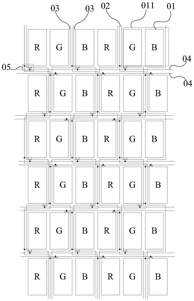
如图1所示,现有触控显示产品一般在阵列基板中由交叉设置的数据信号线02和栅线04划分像素区域,在各像素区域内设置像素电极01,数据信号线02通过开关晶体管05向像素电极01加载数据信号。通常,在数据信号线02的旁边增加触控信号线03,并且采用同一膜层制作完成数据信号线02和触控信号线03。如图1所示,可以看出同一条数据信号线02距离左侧的像素电极01较近,导致像素电极01与数据信号线02之间的耦合电容Cpd较大,容易产生画面显示不良,影响画面显示品质。As shown in FIG. 1 , in the existing touch display products, pixel areas are generally divided by
发明内容SUMMARY OF THE INVENTION
有鉴于此,本发明实施例提供了一种阵列基板、液晶显示面板及显示装置,用以解决现有的阵列基板中数据信号线与像素电极之间的耦合电容较大的问题。In view of this, embodiments of the present invention provide an array substrate, a liquid crystal display panel and a display device to solve the problem of large coupling capacitance between data signal lines and pixel electrodes in the existing array substrate.
因此,本发明实施例提供了一种阵列基板,包括:呈阵列排布的多个像素电极,与各所述像素电极对应连接的数据信号线,以及与所述数据信号线延伸方向一致的触控信号线;其中,Therefore, an embodiment of the present invention provides an array substrate, comprising: a plurality of pixel electrodes arranged in an array, data signal lines correspondingly connected to each of the pixel electrodes, and a contact line consistent with the extending direction of the data signal lines control signal line; among them,
以行方向的每相邻的两个所述像素电极为一电极组,各所述数据信号线位于所述电极组的列间隙处;且在行方向,所述数据信号线与相邻的所述电极组之间均设置有所述触控信号线。Each adjacent two pixel electrodes in the row direction is an electrode group, and each of the data signal lines is located at the column gap of the electrode group; and in the row direction, the data signal lines are connected with the adjacent ones. The touch signal lines are arranged between the electrode groups.
在一种可能的实现方式中,在本发明实施例提供的上述阵列基板中,各所述数据信号线与连接的各所述像素电极之间的距离均相同。In a possible implementation manner, in the above-mentioned array substrate provided in the embodiment of the present invention, the distances between each of the data signal lines and each of the connected pixel electrodes are the same.
在一种可能的实现方式中,在本发明实施例提供的上述阵列基板中,设置有所述数据信号线的所述列间隙的宽度大于所述电极组内像素电极列间隙的宽度。In a possible implementation manner, in the above-mentioned array substrate provided in the embodiment of the present invention, the width of the column gap where the data signal lines are disposed is greater than the width of the pixel electrode column gap in the electrode group.
在一种可能的实现方式中,在本发明实施例提供的上述阵列基板中,所述像素电极在列方向错开X个像素电极的位置,0<X<1。In a possible implementation manner, in the above-mentioned array substrate provided in the embodiment of the present invention, the pixel electrodes are shifted by X pixel electrodes in the column direction, 0<X<1.
在一种可能的实现方式中,在本发明实施例提供的上述阵列基板中,各所述数据信号线与各所述触控信号线沿着直线方向延伸。In a possible implementation manner, in the above-mentioned array substrate provided by the embodiment of the present invention, each of the data signal lines and each of the touch signal lines extend along a linear direction.
在一种可能的实现方式中,在本发明实施例提供的上述阵列基板中,各所述数据信号线与各所述触控信号线沿着折线方向延伸,且该折线方向包括位于不同所述列间隙处和不同行间隙处的多个线段。In a possible implementation manner, in the above-mentioned array substrate provided by the embodiment of the present invention, each of the data signal lines and each of the touch signal lines extend along a folded line direction, and the folded line direction includes positions at different positions on the Multiple line segments at column gaps and at different row gaps.
在一种可能的实现方式中,在本发明实施例提供的上述阵列基板中,所述数据信号线与所述触控信号线分别位于不同的膜层。In a possible implementation manner, in the above-mentioned array substrate provided by the embodiment of the present invention, the data signal lines and the touch signal lines are respectively located in different film layers.
在一种可能的实现方式中,在本发明实施例提供的上述阵列基板中,各所述数据信号线与同一列所述像素电极中的各所述像素电极连接。In a possible implementation manner, in the above-mentioned array substrate provided in the embodiment of the present invention, each of the data signal lines is connected to each of the pixel electrodes in the same column of the pixel electrodes.
在一种可能的实现方式中,在本发明实施例提供的上述阵列基板中,所述数据信号线与所述触控信号线一一对应。In a possible implementation manner, in the above-mentioned array substrate provided in the embodiment of the present invention, the data signal lines correspond to the touch signal lines one-to-one.
在一种可能的实现方式中,在本发明实施例提供的上述阵列基板中,所述阵列基板具有双栅结构;各所述数据信号线与相邻的两列所述像素电极中的各所述像素电极连接。In a possible implementation manner, in the above-mentioned array substrate provided by the embodiment of the present invention, the array substrate has a double gate structure; each of the data signal lines and each of the pixel electrodes in the adjacent two columns The pixel electrodes are connected.
在一种可能的实现方式中,在本发明实施例提供的上述阵列基板中,一条所述数据信号线对应于两条所述触控信号线。In a possible implementation manner, in the above-mentioned array substrate provided in the embodiment of the present invention, one of the data signal lines corresponds to two of the touch signal lines.
另一方面,本发明实施例还提供了一种液晶显示面板,包括本发明实施例提供的上述阵列基板。On the other hand, an embodiment of the present invention further provides a liquid crystal display panel, including the above-mentioned array substrate provided by an embodiment of the present invention.
另一方面,本发明实施例还提供了一种显示装置,包括本发明实施例提供的上述液晶显示面板。On the other hand, an embodiment of the present invention further provides a display device including the above-mentioned liquid crystal display panel provided by the embodiment of the present invention.
本发明实施例的有益效果包括:The beneficial effects of the embodiments of the present invention include:
本发明实施例提供的一种阵列基板、液晶显示面板及显示装置,包括呈阵列排布的多个像素电极,与各像素电极对应连接的数据信号线,以及与数据信号线延伸方向一致的触控信号线;其中,以行方向的每相邻的两个像素电极为一电极组,各数据信号线位于电极组的列间隙处,且在行方向,数据信号线与相邻的电极组之间均设置有触控信号线。由于将数据信号线与两侧的像素电极之间均设置了触控信号线,确保数据信号线始终位于触控信号线远离像素电极的一侧,增大了数据信号线与相邻的像素电极之间的距离,从而极大降低数据信号线与像素电极之间的耦合电容,降低产生画面显示不良的几率,提高了画面显示品质。An array substrate, a liquid crystal display panel, and a display device provided by embodiments of the present invention include a plurality of pixel electrodes arranged in an array, a data signal line corresponding to each pixel electrode, and a contact line consistent with the extending direction of the data signal line. control signal lines; wherein, each adjacent two pixel electrodes in the row direction is an electrode group, each data signal line is located at the column gap of the electrode group, and in the row direction, the data signal line and the adjacent electrode group are A touch signal line is arranged between them. Since the touch signal lines are arranged between the data signal lines and the pixel electrodes on both sides, it is ensured that the data signal lines are always located on the side of the touch signal lines away from the pixel electrodes, which increases the number of data signal lines and adjacent pixel electrodes. Therefore, the coupling capacitance between the data signal line and the pixel electrode is greatly reduced, the probability of poor picture display is reduced, and the picture display quality is improved.
附图说明Description of drawings
图1为现有技术中的阵列基板的结构示意图;FIG. 1 is a schematic structural diagram of an array substrate in the prior art;
图2为本发明实施例提供的阵列基板的结构示意图之一;FIG. 2 is a schematic structural diagram of an array substrate provided by an embodiment of the present invention;
图3为本发明实施例提供的阵列基板的结构示意图之二;FIG. 3 is a second schematic structural diagram of an array substrate provided by an embodiment of the present invention;
图4为本发明实施例提供的阵列基板的结构示意图之三;FIG. 4 is a third schematic structural diagram of an array substrate provided by an embodiment of the present invention;
图5为本发明实施例提供的阵列基板的结构示意图之四;FIG. 5 is a fourth schematic structural diagram of an array substrate according to an embodiment of the present invention;
图6为本发明实施例提供的阵列基板的结构示意图之五。FIG. 6 is a fifth schematic structural diagram of an array substrate provided by an embodiment of the present invention.
具体实施方式Detailed ways
下面结合附图,对本发明实施例提供的阵列基板、液晶显示面板及显示装置的具体实施方式进行详细地说明。The specific implementations of the array substrate, the liquid crystal display panel and the display device provided by the embodiments of the present invention will be described in detail below with reference to the accompanying drawings.
附图中各部件的形状和大小不反映阵列基板的真实比例,目的只是示意说明本发明内容。The shapes and sizes of the components in the drawings do not reflect the actual scale of the array substrate, and are only intended to illustrate the content of the present invention.
因此,本发明实施例提供了一种阵列基板,如图2至图6所示,包括:呈阵列排布的多个像素电极01,与各像素电极01对应连接的数据信号线02,以及与数据信号线02延伸方向一致的触控信号线03;其中,Therefore, an embodiment of the present invention provides an array substrate, as shown in FIG. 2 to FIG. 6 , comprising: a plurality of
以行方向的每相邻的两个像素电极01为一电极组011,各数据信号线02位于电极组011的列间隙处;且在行方向,数据信号线02与相邻的各电极组011之间均设置有触控信号线03。Taking every two
具体地,在本发明实施例提供上述阵列基板中,由于将数据信号线02与两侧的像素电极01之间均设置了触控信号线03,确保数据信号线02始终位于触控信号线03远离像素电极01的一侧,增大了数据信号线02与相邻的像素电极01之间的距离,从而极大降低数据信号线02与像素电极01之间的耦合电容Cpd,降低产生画面显示不良的几率,提高了画面显示品质。Specifically, in the above-mentioned array substrate provided by the embodiment of the present invention, since the
可选地,在本发明实施例提供上述阵列基板中,通过将数据信号线02设置为始终位于触控信号线03远离像素电极01的一侧,可以使数据信号线02与相邻的像素电极01之间的距离在大于0且小于等于15μm的范围。Optionally, in the above-mentioned array substrate provided in the embodiment of the present invention, by arranging the
在现有的阵列基板中,如图1所示,同一条数据信号线02与两侧的像素电极01间距不一致,距离左侧的像素电极01较近,距离右侧的像素电极01较远,这会导致耦合电容Cpd差异很大,进而也会产生画面显示不良,影响画面显示品质。In the existing array substrate, as shown in FIG. 1 , the distance between the same
基于此,可选地,在本发明实施例提供的上述阵列基板中,如图2至图6所示,各数据信号线02与连接的各像素电极01之间的距离均相同。Based on this, optionally, in the above-mentioned array substrate provided in the embodiment of the present invention, as shown in FIG. 2 to FIG. 6 , the distances between each
具体地,由于将各数据信号线02与连接的各像素电极01之间的距离均设置为相同,可以保证各数据信号线02与最邻近的一列像素电极01(一般为连接的像素电极01)之间具有相同的耦合电容Cpd,减少了不同的数据信号线02与像素电极01之间的耦合电容差异而产生的画面显示不良,提升了画面品质。Specifically, since the distances between each
可选地,在本发明实施例提供的上述阵列基板中,如图2至图6所示,以行方向的每相邻的两个像素电极01为一电极组011,各数据信号线02位于电极组011的列间隙处,可以认为,在每行像素电极01中,仅在间隔的像素电极列间隙处设置有数据信号线02。Optionally, in the above-mentioned array substrate provided by the embodiment of the present invention, as shown in FIG. 2 to FIG. 6 , each adjacent two
具体地,如图2和图3所示,可以仅在每行的奇数像素电极列间隙处设置数据信号线02,这样偶数像素电极列间隙处未设置数据信号线02,此种情况可以认为各组电极组011对齐排列。如图4至图5所示,可以仅在奇数行的偶数像素电极列间隙处设置数据信号线02,这样奇数行的奇数像素电极列间隙处未设置数据信号线02,并且,在偶数行的奇数像素电极列间隙处设置数据信号线02,这样偶数行的偶数像素电极列间隙处未设置数据信号线02,此种情况可以认为各行电极组011在列方向错开排列。如图6所示,可以仅在第一、二、五和六行的偶数像素电极列间隙处设置数据信号线02,这样第一、二、五和六行的奇数像素电极列间隙处未设置数据信号线02,并且,在第三和四行的奇数像素电极列间隙处设置数据信号线02,这样第三和四行的偶数像素电极列间隙处未设置数据信号线02,此种情况可以认为每两行电极组011在列方向错开排列。并且,在未设置数据信号线02的像素电极列间隙处,还可以根据实际需要设置其他信号线,例如触控信号线03或者检测信号线等,在此不做限定。Specifically, as shown in FIG. 2 and FIG. 3 , the
可选地,在本发明实施例提供的上述阵列基板中,如图2至图5所示,设置有数据信号线02的列间隙的宽度大于电极组011内像素电极列间隙的宽度。Optionally, in the above-mentioned array substrate provided by the embodiment of the present invention, as shown in FIG. 2 to FIG. 5 , the width of the column gap in which the
具体地,尽可能的缩小未设置数据信号线02的像素电极列间隙宽度,可以增大像素电极01的使用面积,从而提高像素的开口率。当然,在具体应用时,如图6所示,也可以将各像素电极列间隙的宽度设置为相同,在此不做限定。Specifically, the gap width of the pixel electrode column where the
可选地,在本发明实施例提供的上述阵列基板中,如图4和图5所示,在设置有数据信号线02的列间隙的宽度大于电极组内像素电极列间隙的宽度的基础上,可以设计像素电极01在列方向错开X个像素电极的位置,0<X<1,即在列方向,存在像素电极01不对齐排列的情况。这样可以减弱由于像素电极列间隙的宽度不同而引起的视觉效应。Optionally, in the above-mentioned array substrate provided by the embodiment of the present invention, as shown in FIG. 4 and FIG. 5 , on the basis that the width of the column gap where the
可选地,在本发明实施例提供的上述阵列基板中,如图2和图3所示,各数据信号线02与各触控信号线03可以沿着直线方向延伸。Optionally, in the above-mentioned array substrate provided by the embodiment of the present invention, as shown in FIG. 2 and FIG. 3 , each data signal
具体地,当各数据信号线02与各触控信号线03沿着直线方向延伸时,可以保证各数据信号线02与各触控信号线03的布线长度最小,有利于布线设计。但会在间隔的整列像素电极01的间隙处存在未设置任何数据信号线02的情况,由于设置数据信号线02的像素电极列间隙宽度通常大于未设置数据信号线02的像素电极列间隙宽度,而间隔的整列间隙不均匀排布不利于画面显示的视觉效果。Specifically, when each data signal
可选地,在本发明实施例提供的上述阵列基板中,如图4和图5所示,各数据信号线02与各触控信号线03可以沿着折线方向延伸,且该折线方向包括位于不同列间隙处和不同行间隙处的多个线段。Optionally, in the above-mentioned array substrate provided by the embodiment of the present invention, as shown in FIG. 4 and FIG. 5 , each data signal
具体地,当数据信号线02与触控信号线03沿着折线方向延伸时,可以认为数据信号线02与触控信号线03均呈“弓”字形设计。这样可以优化像素排列,可以减弱由于像素电极列间隙的宽度不同而引起的视觉效应。Specifically, when the
可选地,在本发明实施例提供的上述阵列基板中,如图4和图5所示,在每相邻的两行像素电极中,设置有数据信号线02的像素电极列间隙的位置互不相同,例如在奇数行的偶数像素电极列间隙处设置数据信号线02,奇数行的奇数像素电极列间隙处未设置数据信号线02,并且,在偶数行的奇数像素电极列间隙处设置数据信号线02,偶数行的偶数像素电极列间隙处未设置数据信号线02;即沿着折线方向延伸的每条数据信号线02在每行像素电极01处均进行转折。或者,可以认为,各行电极组011在列方向错开一个像素电极左右的位置排列。Optionally, in the above-mentioned array substrate provided by the embodiment of the present invention, as shown in FIG. 4 and FIG. 5 , in every two adjacent rows of pixel electrodes, the positions of the pixel electrode column gaps where the data signal
当然,沿着折线方向延伸的每条数据信号线02也可以在任意行像素电极01处进行转折,例如图6所示,每条数据信号线02可以每两行像素电极01处进行转折,在此不做限定。Of course, each data signal
可选地,在本发明实施例提供的上述阵列基板中,数据信号线02与触控信号线02分别位于不同的膜层,以确保两者在交叉位置处不会发生短路。Optionally, in the above-mentioned array substrate provided in the embodiment of the present invention, the data signal
可选地,在本发明实施例提供的上述阵列基板中,如图2和图4所示,各数据信号线02与同一列像素电极01中的各像素电极01连接,即数据信号线02与像素电极01列之间为一一对应关系。此时,阵列基板一般为单栅结构,即一行像素电极01中的各像素电极01通过对应的各开关晶体管05与一条栅线04连接。Optionally, in the above-mentioned array substrate provided by the embodiment of the present invention, as shown in FIG. 2 and FIG. 4 , each data signal
具体地,当各数据信号线02与各触控信号线03沿着直线方向延伸时,如图2所示,数据信号线02位于连接的像素电极01列的一侧。当各数据信号线02与各触控信号线03沿着折线方向延伸时,如图4所示,数据信号线02位于连接的像素电极01列的两侧。Specifically, when each data signal
可选地,在本发明实施例提供的上述阵列基板中,在阵列基板为单栅结构时,数据信号线02可以与触控信号线02一一对应。Optionally, in the above-mentioned array substrate provided by the embodiment of the present invention, when the array substrate has a single-gate structure, the data signal
具体地,如图2和图4所示,仅在数据信号线02与连接的像素电极01之间设置触控信号线03,未设置数据信号线02的像素电极列间隙处不会设置触控信号线03,保证未设置数据信号线02的像素电极列间隙可以具有最小的宽度,这样可以尽量增大像素开口率。Specifically, as shown in FIG. 2 and FIG. 4 , the
可选地,在本发明实施例提供的上述阵列基板中,如图3和图5所示,阵列基板也可以具有双栅结构,即一行像素电极01中的各像素电极01通过对应的各开关晶体管05分别与两条栅线04连接,这样可以节约一半的数据信号线02,从而有利于提高开口率;此时,各数据信号线02与相邻的两列像素电极01中的各像素电极01连接。Optionally, in the above-mentioned array substrate provided in the embodiment of the present invention, as shown in FIG. 3 and FIG. 5 , the array substrate may also have a double gate structure, that is, each
可选地,在本发明实施例提供的上述阵列基板中,如图3和图5所示,一条数据信号线02对应于两条触控信号线03。Optionally, in the above-mentioned array substrate provided in the embodiment of the present invention, as shown in FIG. 3 and FIG. 5 , one
具体地,如图3和图5所示,仅在数据信号线02与连接的像素电极01之间设置触控信号线03,未设置数据信号线02的像素电极列间隙处不会设置触控信号线03,保证未设置数据信号线02的像素电极列间隙可以具有最小的宽度,这样可以尽量增大像素开口率。Specifically, as shown in FIG. 3 and FIG. 5 , the
基于同一发明构思,本发明实施例还提供了一种液晶显示面板,包括本发明实施例提供的上述阵列基板。由于该液晶显示面板解决问题的原理与前述一种阵列基板相似,因此该液晶显示面板的实施可以参见阵列基板的实施,重复之处不再赘述。Based on the same inventive concept, an embodiment of the present invention further provides a liquid crystal display panel, including the above-mentioned array substrate provided by an embodiment of the present invention. Since the principle of solving the problem of the liquid crystal display panel is similar to that of the aforementioned array substrate, the implementation of the liquid crystal display panel can refer to the implementation of the array substrate, and the repetition will not be repeated.
基于同一发明构思,本发明实施例还提供了一种显示装置,包括本发明实施例提供的上述液晶显示面板,该显示装置可以为:手机、平板电脑、电视机、显示器、笔记本电脑、数码相框、导航仪等任何具有显示功能的产品或部件。该显示装置的实施可以参见上述液晶显示面板的实施例,重复之处不再赘述。Based on the same inventive concept, an embodiment of the present invention also provides a display device, including the above-mentioned liquid crystal display panel provided by the embodiment of the present invention, and the display device may be: a mobile phone, a tablet computer, a TV, a monitor, a notebook computer, a digital photo frame , navigator and any other product or component with display function. For the implementation of the display device, reference may be made to the above-mentioned embodiments of the liquid crystal display panel, and repeated descriptions will not be repeated.
本发明实施例提供的上述阵列基板、液晶显示面板及显示装置,包括呈阵列排布的多个像素电极,与各像素电极对应连接的数据信号线,以及与数据信号线延伸方向一致的触控信号线;其中,以行方向的每相邻的两个像素电极为一电极组,各数据信号线位于电极组的列间隙处,且在行方向数据信号线与相邻的电极组之间均设置有触控信号线。由于将数据信号线与两侧的像素电极之间均设置了触控信号线,确保数据信号线始终位于触控信号线远离像素电极的一侧,增大了数据信号线与相邻的像素电极之间的距离,从而极大降低数据信号线与像素电极之间的耦合电容,降低产生画面显示不良的几率,提高了画面显示品质。The above-mentioned array substrate, liquid crystal display panel, and display device provided by the embodiments of the present invention include a plurality of pixel electrodes arranged in an array, a data signal line corresponding to each pixel electrode, and a touch control line consistent with the extending direction of the data signal line. Signal lines; wherein, each adjacent two pixel electrodes in the row direction is an electrode group, and each data signal line is located at the column gap of the electrode group, and between the data signal line in the row direction and the adjacent electrode groups A touch signal line is provided. Since the touch signal lines are arranged between the data signal lines and the pixel electrodes on both sides, it is ensured that the data signal lines are always located on the side of the touch signal lines away from the pixel electrodes, which increases the number of data signal lines and adjacent pixel electrodes. Therefore, the coupling capacitance between the data signal line and the pixel electrode is greatly reduced, the probability of poor picture display is reduced, and the picture display quality is improved.
显然,本领域的技术人员可以对本发明进行各种改动和变型而不脱离本发明的精神和范围。这样,倘若本发明的这些修改和变型属于本发明权利要求及其等同技术的范围之内,则本发明也意图包含这些改动和变型在内。It will be apparent to those skilled in the art that various modifications and variations can be made in the present invention without departing from the spirit and scope of the invention. Thus, provided that these modifications and variations of the present invention fall within the scope of the claims of the present invention and their equivalents, the present invention is also intended to include these modifications and variations.
Claims (13)
Priority Applications (2)
| Application Number | Priority Date | Filing Date | Title |
|---|---|---|---|
| CN201711022303.3A CN107817926B (en) | 2017-10-27 | 2017-10-27 | Array substrate, liquid crystal display panel and display device |
| US15/919,363 US10585314B2 (en) | 2017-10-27 | 2018-03-13 | Array substrate, liquid crystal display panel and display apparatus |
Applications Claiming Priority (1)
| Application Number | Priority Date | Filing Date | Title |
|---|---|---|---|
| CN201711022303.3A CN107817926B (en) | 2017-10-27 | 2017-10-27 | Array substrate, liquid crystal display panel and display device |
Publications (2)
| Publication Number | Publication Date |
|---|---|
| CN107817926A CN107817926A (en) | 2018-03-20 |
| CN107817926B true CN107817926B (en) | 2021-03-23 |
Family
ID=61603100
Family Applications (1)
| Application Number | Title | Priority Date | Filing Date |
|---|---|---|---|
| CN201711022303.3A Active CN107817926B (en) | 2017-10-27 | 2017-10-27 | Array substrate, liquid crystal display panel and display device |
Country Status (2)
| Country | Link |
|---|---|
| US (1) | US10585314B2 (en) |
| CN (1) | CN107817926B (en) |
Families Citing this family (10)
| Publication number | Priority date | Publication date | Assignee | Title |
|---|---|---|---|---|
| US10803818B2 (en) * | 2018-10-24 | 2020-10-13 | HKC Corporation Limited | Pixel architecture, display substrate, and display |
| CN110085125B (en) * | 2019-05-05 | 2021-10-15 | 京东方科技集团股份有限公司 | Array substrate and driving method thereof, display panel and display device |
| CN112526778B (en) * | 2019-09-19 | 2024-06-28 | 群创光电股份有限公司 | Display device and touch display device |
| CN113325638B (en) * | 2020-02-28 | 2025-04-25 | 京东方科技集团股份有限公司 | Array substrate and display device |
| CN113820893B (en) | 2020-06-18 | 2022-12-20 | 京东方科技集团股份有限公司 | Display panel and display device |
| CN112034656B (en) * | 2020-09-11 | 2022-08-26 | 合肥鑫晟光电科技有限公司 | Array substrate and display device |
| CN112328117B (en) * | 2020-11-17 | 2023-12-12 | 武汉华星光电半导体显示技术有限公司 | Touch display substrate, touch display panel and touch display device |
| CN113253530B (en) * | 2021-07-14 | 2021-09-17 | 北京京东方技术开发有限公司 | Display panel and display device |
| WO2025059799A1 (en) * | 2023-09-18 | 2025-03-27 | 京东方科技集团股份有限公司 | Touch-control display substrate and touch-control display apparatus |
| JP7703626B2 (en) * | 2023-12-12 | 2025-07-07 | シャープディスプレイテクノロジー株式会社 | Active matrix substrate, in-cell touch panel, and display device |
Family Cites Families (40)
| Publication number | Priority date | Publication date | Assignee | Title |
|---|---|---|---|---|
| JP3358744B2 (en) * | 1993-05-06 | 2002-12-24 | シャープ株式会社 | Liquid crystal display |
| AU2002336341A1 (en) * | 2002-02-20 | 2003-09-09 | Planar Systems, Inc. | Light sensitive display |
| KR101100884B1 (en) * | 2004-11-08 | 2012-01-02 | 삼성전자주식회사 | Display devices and drive devices for display devices |
| US20070109239A1 (en) * | 2005-11-14 | 2007-05-17 | Den Boer Willem | Integrated light sensitive liquid crystal display |
| KR101349096B1 (en) * | 2006-12-27 | 2014-01-09 | 삼성디스플레이 주식회사 | Display device |
| KR101338011B1 (en) * | 2007-01-25 | 2013-12-06 | 삼성디스플레이 주식회사 | Display device |
| JP4862777B2 (en) * | 2007-08-10 | 2012-01-25 | カシオ計算機株式会社 | Display device |
| US20090115735A1 (en) * | 2007-11-06 | 2009-05-07 | Himax Technologies Limited | Sensor with pressure-induced varied capacitance |
| KR20090075369A (en) * | 2008-01-04 | 2009-07-08 | 삼성전자주식회사 | Display panel |
| KR101458569B1 (en) * | 2008-03-13 | 2014-11-12 | 삼성디스플레이 주식회사 | Display device |
| TWI417766B (en) * | 2008-05-23 | 2013-12-01 | Innolux Corp | Touch-sensitive liquid crystal display device and method for driving same |
| US8098345B2 (en) * | 2008-11-21 | 2012-01-17 | Sharp Kabushiki Kaisha | Liquid crystal display device and electronics device |
| JP2010185944A (en) * | 2009-02-10 | 2010-08-26 | Toshiba Mobile Display Co Ltd | Liquid crystal display element |
| TWI396011B (en) * | 2009-06-16 | 2013-05-11 | Au Optronics Corp | Touch panel |
| CN102023429B (en) * | 2009-09-17 | 2013-10-23 | 北京京东方光电科技有限公司 | TFT-LCK array substrate and method for manufacturing same and method for repairing broken lines |
| US8018399B2 (en) * | 2009-11-18 | 2011-09-13 | Century Display(ShenZhen) Co., Ltd. | Pixel array |
| KR101761861B1 (en) * | 2010-06-18 | 2017-07-27 | 삼성디스플레이 주식회사 | Touch sensible display device |
| KR101726739B1 (en) * | 2010-12-21 | 2017-04-14 | 삼성디스플레이 주식회사 | Touch display substrate and touch display panel having the same |
| CN102629607B (en) * | 2012-02-09 | 2016-02-10 | 京东方科技集团股份有限公司 | Array base palte and dual field of view display device and manufacture method thereof |
| CN102937852B (en) * | 2012-10-19 | 2015-08-05 | 北京京东方光电科技有限公司 | A kind of capacitance type in-cell touch panel, its driving method and display device |
| CN102955637B (en) * | 2012-11-02 | 2015-09-09 | 北京京东方光电科技有限公司 | A kind of capacitance type in-cell touch panel, its driving method and display device |
| KR101906248B1 (en) * | 2012-12-13 | 2018-10-11 | 엘지디스플레이 주식회사 | Liquid crystal display device |
| CN103558946A (en) * | 2013-11-15 | 2014-02-05 | 京东方科技集团股份有限公司 | Touch structure, liquid crystal panel and display device |
| CN103728761B (en) * | 2013-12-26 | 2016-07-13 | 深圳市华星光电技术有限公司 | An embedded touch array substrate and liquid crystal display panel |
| CN103728760A (en) * | 2013-12-26 | 2014-04-16 | 深圳市华星光电技术有限公司 | Touch liquid crystal display and array substrate thereof |
| CN103728762A (en) * | 2013-12-26 | 2014-04-16 | 深圳市华星光电技术有限公司 | Touch liquid crystal display and array substrate thereof |
| CN103760703A (en) * | 2013-12-30 | 2014-04-30 | 深圳市华星光电技术有限公司 | Embedded touch device of double-gate panel |
| CN103676388A (en) * | 2013-12-30 | 2014-03-26 | 合肥京东方光电科技有限公司 | Array substrate, display panel, display method of display panel and display device |
| CN103955309B (en) * | 2014-04-14 | 2017-08-25 | 京东方科技集团股份有限公司 | Display panel and its driving method, display device |
| CN104090697B (en) * | 2014-06-30 | 2017-02-08 | 京东方科技集团股份有限公司 | Capacitance type embedded touch screen and touch location method and display device of capacitance type embedded touch screen |
| CN104657024A (en) * | 2015-03-13 | 2015-05-27 | 京东方科技集团股份有限公司 | Built-in touch screen and display device |
| CN104793812B (en) * | 2015-04-13 | 2017-01-25 | 京东方科技集团股份有限公司 | A kind of OLED display substrate, touch display panel and display device |
| CN104934008A (en) * | 2015-07-09 | 2015-09-23 | 京东方科技集团股份有限公司 | Array substrate and driving method thereof, display panel and display apparatus |
| CN105093611B (en) * | 2015-07-21 | 2018-09-11 | 京东方科技集团股份有限公司 | A kind of array substrate and its driving method, display panel, display device |
| KR102485387B1 (en) * | 2016-01-20 | 2023-01-06 | 삼성디스플레이 주식회사 | Display device |
| KR102435900B1 (en) * | 2016-01-21 | 2022-08-26 | 삼성디스플레이 주식회사 | Display device |
| CN105511688B (en) * | 2016-01-29 | 2018-06-19 | 上海天马微电子有限公司 | Array substrate, display and electronic equipment |
| CN105629612B (en) * | 2016-03-14 | 2019-04-05 | 昆山龙腾光电有限公司 | Thin-film transistor array base-plate and preparation method thereof |
| CN105652498A (en) * | 2016-03-22 | 2016-06-08 | 上海中航光电子有限公司 | Array substrate, touch display panel and touch display device |
| US10203530B1 (en) * | 2017-11-28 | 2019-02-12 | Shenzhen China Star Optoelectronics Semiconductor Display Technology Co., Ltd. | Pixel driving circuit and LCD panel |
-
2017
- 2017-10-27 CN CN201711022303.3A patent/CN107817926B/en active Active
-
2018
- 2018-03-13 US US15/919,363 patent/US10585314B2/en active Active
Also Published As
| Publication number | Publication date |
|---|---|
| US10585314B2 (en) | 2020-03-10 |
| US20190129258A1 (en) | 2019-05-02 |
| CN107817926A (en) | 2018-03-20 |
Similar Documents
| Publication | Publication Date | Title |
|---|---|---|
| CN107817926B (en) | Array substrate, liquid crystal display panel and display device | |
| CN105609037B (en) | A kind of array substrate, touch-control display panel and touch control display apparatus | |
| US10649289B2 (en) | Array substrate, display panel and display device | |
| CN104898343B (en) | Array base palte, display panel and display device | |
| US10884562B2 (en) | Touch substrate, touch control display panel, and touch control display apparatus | |
| US10082905B2 (en) | Touch control display panel and touch control display device | |
| US20170031223A1 (en) | Array substrate, liquid crystal display panel and display device | |
| US9176350B2 (en) | Pixel array and liquid crystal display device | |
| CN106707646A (en) | Array base plate and display panel | |
| CN105467643B (en) | Integrated touch display panel and touch display device | |
| CN104503633A (en) | Embedded touch screen, drive method thereof and display device | |
| US20160358570A1 (en) | Display apparatus | |
| CN108594552B (en) | Display substrate, display panel, display device and driving method thereof | |
| TWI537641B (en) | Fan-out wire structure and display panel thereof | |
| US20190088681A1 (en) | Array substrate, method for manufacturing the same, and display device | |
| US10042494B2 (en) | Array substrate, touch display panel and touch display device | |
| CN105974686A (en) | Array substrate and display panel | |
| JP2020525807A (en) | Array substrate and display device | |
| CN103926768B (en) | A kind of array base palte, display floater and display device | |
| CN104730781A (en) | ADS array substrate, manufacturing method thereof, and display device comprising same | |
| CN107068046A (en) | Display panel and display device | |
| CN109614009B (en) | Touch display panel and touch display device | |
| US20200310572A1 (en) | Touch substrate, display panel and display device | |
| US9425166B2 (en) | GOA layout method, array substrate and display device | |
| CN209044564U (en) | A kind of array substrate, In-cell touch panel and display device |
Legal Events
| Date | Code | Title | Description |
|---|---|---|---|
| PB01 | Publication | ||
| PB01 | Publication | ||
| SE01 | Entry into force of request for substantive examination | ||
| SE01 | Entry into force of request for substantive examination | ||
| GR01 | Patent grant | ||
| GR01 | Patent grant |