Detailed Description
Example embodiments of the present disclosure include systems, devices, and methods for photonic fused three-dimensional or "3D" printing using powdered, pasty, or liquid fusible materials. In such embodiments, the layers of fusible material are built upon one another. The structure of each layer is defined by printing or otherwise applying a pattern using an inhibiting material, such as a non-fusing absorptive material, a non-fusing reflective material, or a material that chemically or physically inhibits the fusible material from fusing.
Each combined layer of fusible material and inhibiting material may be exposed to photonic energy. As used herein, the terms "photonic energy" and "photonic fusion" refer to energy or processes involving incoherent light emission having a spectral range of about 0.2 microns to 1.5 microns. In various embodiments, the photonic energy may be applied to all or a portion of the uppermost layer simultaneously in a controlled burst or flash (flash). In response to photon energy, the areas of the uppermost layer of fusible material that are not masked or inhibited by the inhibiting material may be purified, fused, melted, vaporized, or melted. In some examples, the fusion of the fusible material in response to photonic energy may occur on an intralayer and interlayer basis. In such embodiments, the regions of fusible material masked/inhibited by the inhibiting material may remain in an unfused state. Specific details of three-dimensional printing processes and apparatus are described in more detail herein with reference to various examples and figures.
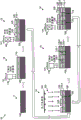
Fig. 1 illustrates an example process 10 for generating a three-dimensional object using photon fusion, in accordance with various embodiments of the present disclosure. As shown, the process 10 may begin by providing a substrate 105 at reference numeral 11. In some embodiments, the substrate 105 may be composed of and/or include materials similar to the fusible materials used in other parts of the process. For example, the substrate 105 may include a metal, plastic, wood, glass, ceramic, or other material substrate formed in a separate process.
The substrate 105 may include a disposable and/or reusable platform that a corresponding three-dimensional printing device may manipulate while handling other processes of three-dimensional printing. For example, the substrate 105 may be moved in multiple dimensions by a three-dimensional printer as required by the processes described herein. For example, the substrate 105 may be moved relative to other elements of the three-dimensional printer to facilitate, improve, or optimize the results of various three-dimensional printing processes.
At reference numeral 12, the example process 10 can include laying down a layer of fusible material 110 using a fusible material applicator 130. In some examples, the fusible material applicator 130 can include a printhead-type applicator that moves relative to the substrate 105 in a direction such as 131. In some embodiments, the fusible material applicator 130 can include a substrate wide arrangement such that the layer 110 can be laid down in a single pass over a substrate 105 having particular dimensions. For example, the fusible material applicator 130 may include a "page wide array" of nozzles or openings that release the layer of fusible material 110 on the substrate 105 as it moves in the direction indicated by arrow 131.
To achieve a variable thickness layer of fusible material 110, the fusible material applicator 130 can make multiple passes over the substrate 100 to tend to build the layer to a particular thickness. In other examples, the rate at which the layer of fusible material 110 is lowered by the fusible material applicator 130 may be adjusted to achieve a particular thickness. Thus, embodiments of the present invention may coat a layer of fusible material as thin as one particle of fusible material.
Once the layer of fusible material 110 is laid down, the inhibiting material applicator 140 may lay down the patterned layer of inhibiting material 120 at the reference mark 13. In one example, the pattern of the patterned suppression material layer 120 may include a negative of the desired layer to be fused in that particular layer of the three-dimensional object. In this way, the patterned inhibiting material layer 120 may establish a plurality of exposed regions 125 of the fusible material layer 110 and corresponding blocked regions of the fusible material 110 under the area covered by the inhibiting material 120 or in contact with the inhibiting material 120. The patterned suppression material layer 120 may be based on a corresponding model of the desired three-dimensional object.
The inhibiting material applicator 140 may include any type of printing device capable of applying a pattern of inhibiting material 120 on the layer of fusible material 110. For example, the inhibiting material applicator 140 may include an inkjet (e.g., thermal inkjet, piezo inkjet, etc.) or a spray that may selectively apply a liquid or semi-liquid (e.g., gel) layer 120 of inhibiting material onto the fusible material layer 110.
The inhibiting material applicator 140 may be movable relative to the substrate 105 and/or the layer of fusible material 110 along a direction 141. In various examples, direction 141 may include a two-dimensional or three-dimensional degree of freedom through which inhibiting material 120 is applied. In some embodiments, the inhibiting material applicator 140 may include a page wide array print head or a scanning print head that moves across one dimension of the layer of fusible material 110 while scanning across another dimension. In any such embodiment, the distance between the inhibiting material applicator 140 and the fusible material layer 110 can be varied to accommodate and/or optimize the quality of the application of the inhibiting material 120. For example, when building the layer of fusible material 110 and the layer of inhibiting material 120, example embodiments of the present disclosure may include moving the inhibiting material applicator 140 further away from the substrate 105 to provide clearance.
At reference numeral 14, the inhibiting material layer 120 of the fusible material layer 110 can be exposed to photonic energy 151 emitted by the photon emitter 150. In some embodiments, the photonic energy is provided by an incoherent light source. For example, the incoherent light source may comprise a xenon (Xe) source. Such Xe sources can emit incoherent photon energy (e.g., electromagnetic radiation) in the 150nm to 1100nm range with radiation peaks below 1 micron (e.g., 475nm, 827nm, 885nm, 919nm, and 980nm) in the visible and near IR.
Photonic energy may be delivered in short pulses simultaneously across some or all of the surfaces of the inhibiting material 120 and the uppermost layer of fusible material 110. In some embodiments, the pulse of photon energy is less than 1 millisecond. Such short pulses may be used to ensure that only a single top layer of fusible material is heated to the melting point without dissipating energy due to heating of the underlying layer or due to significant radiation into the air. Thus, embodiments using short pulses of photonic energy 151 allow for melting of particles while using relatively low power densities.
The portion of the uppermost layer of the fusible material layer 110 below the region 125 is exposed by the pattern of the inhibiting material layer 120, and the inhibiting material layer 120 may react to photon energy 151 by heating to a temperature at which the fusible material 110 fuses. In some embodiments, the regions of the fusible material layer 110 under the pattern of the inhibit layer 120 are protected from the photon energy 151 and thus do not fuse.
Embodiments of the present disclosure may include a restraining material 120 that uses various mechanisms to restrain the fusion of the fusible material 110. In an example embodiment, the inhibiting material 120 may include a material that reflects or absorbs electromagnetic radiation within the spectral range of the photon emitter 150.
In one example, the inhibiting material 120 may include a white ink including a reflective additive, such as titanium oxide (TiO 2). Example white inks can reflect electromagnetic radiation in the UV, visible, and near IR regions while transmitting wavelengths above 1 micron. In other embodiments, the inhibiting material 120 may include a multilayer structure that provides an interference filter that selectively reflects electromagnetic radiation of the photon emitter 150. For example, the reflective material may include layers of different materials applied by a suppression material applicator that combine to form an interference dielectric mirror having a stop band corresponding to the spectral range of the photon emitter 150. In such embodiments, photon energy 151 incident on the surface of the reflective material is reflected off of the underlying fusible material 110, thereby masking the underlying fusible material 110.
In another example, the inhibiting material 120 may include a material that rapidly absorbs photon energy 151 but does not fuse or otherwise be a thermal insulator or nonconductor. For example, the inhibiting material layer 120 may include a material layer that: which absorbs electromagnetic radiation (e.g., Xe radiation) from the photon emitter 150, melts and/or evaporates during the light pulse, thereby shielding the underlying fusible material layer 110 from fusing. Exemplary absorbing materials that evaporate in response to applied photonic energy include, but are not limited to, polymers, latexes, and the like.
In yet another example, the inhibiting material 120 may include a chemical or physical property that affects the underlying fusible material, preventing it from fusing in response to the photonic energy 151.
As illustrated at reference numeral 15, the regions 115 of the fusible material 110 left exposed by the gaps 125 in the patterned inhibiting material layer 120 may be fused by the photon energy 151 to form solid components in the fusible material layer 110. To form the next layer of the three-dimensional object, the fusible material applicator 130 may deposit another layer of fusible material, here designated as fusible material layer 110-2. As shown, a layer of fusible material 110-2 can be laid down over the first layer of fusible material 110-1 and the patterned layer of inhibiting material 120. As shown, the subsequent layer of fusible material 110-2 can fill in the gap (previously designated 125) while maintaining a substantially planar upper surface.
In the event that a subsequent layer of fusible material 110-2 is applied to the previously applied layer of fusible material 110-1 and layer of inhibiting material 120, the inhibiting material applicator 140 may apply another patterned layer of inhibiting material 120 according to the corresponding model of the three-dimensional object. As with the previously patterned inhibiting material layer 120, the uppermost patterned inhibiting material layer 120 may be left with a gap 125 to establish an exposed layer of the fusible material layer 110-2. At this time, the process depicted at reference numerals 14, 15, and 16 may be repeated to successively build the three-dimensional object 115 of fusible material.
The wavelength, intensity, and/or duration of the photonic energy 151 may vary based on the material properties of the restraining material layer 120 and/or the fusible material layer 110. For example, photonic energy 151 emitted by photonic emitter 150 may include high intensity photonic energy that may be delivered in short pulses. In some embodiments, the pulses may be delivered as a series of short pulses. In such embodiments, the duration and intensity of the photonic energy 151 may help to remove unwanted impurities from the fusible material 110, faster fusing of the fusible material 110, limit heat leakage (cladding), and promote fusion between layers of the fusible material 110.
In various embodiments, the material and thickness between layers of the fusible material 110 may be varied to form alloys or semi-alloys in the resulting three-dimensional object. Fig. 2 depicts an example of alloy formation according to various embodiments of the present disclosure. As shown in the cross-sectional view at reference numeral 20, a plurality of fusible material layers 110-1 and 110-2 are constructed to create a fused material region 115. A subsequent layer of fusible material 111 is placed over the fused material region 115 and another patterned layer of inhibiting material 120 is placed over the fusible material layer 111 to create an exposed region 125. In such embodiments, the fusible material 110 and the fusible material 111 may be different. For example, the fusible material may comprise one metal, while the fusible material layer 111 may comprise a different metal. When the fusible material layer 111 is exposed to photonic energy 151, portions may fuse and/or bond with the underlying previously fused fusible material layer 110 to create a localized alloy.
At reference numeral 21, the stack of materials may be exposed to a photon injection process according to various embodiments described herein. In response to the photonic energy 151, the exposed regions of the fusible material layer 111 can fuse to generate fused fusible material regions 117 and fused fusible material regions 116. The fused fusible material region 116 can include a mixture of fusible materials 110 and 111. In this manner, various fused fusible material regions may be established to have particular alloy properties based on the use of different fusible materials within the layers of the resulting three-dimensional object.
Fig. 3 depicts a schematic diagram of a three-dimensional printer 300. As shown, the three-dimensional printer 300 may include a processor 310 for executing machine-readable executable code stored in a memory 330 to carry out operations and control other components of the three-dimensional printer 300. In various examples, processor 310 may be a microprocessor, a microcontroller, an Application Specific Integrated Circuit (ASIC), and the like. According to an example embodiment, the processor 310 is a hardware component, such as a circuit. Memory 330 may include volatile or non-volatile memory, such as Dynamic Random Access Memory (DRAM), electrically erasable programmable read-only memory (EEPROM), Magnetoresistive Random Access Memory (MRAM), memristors, flash memory, floppy disks, compact disk read-only memory (CD-ROM), digital video disk read-only memory (DVD-ROM), or other optical or magnetic media on which executable code may be stored, among others.
The processor 310 may execute the three-dimensional printing code 331. The three-dimensional printing code 331 may include instructions for generating control signals that cause the suppression material applicator 140, the photonic energy emitter 150, and/or the fusible material applicator 130 to implement corresponding operations of a three-dimensional printing process according to various embodiments of the present disclosure. For example, the instructions included in the three-dimensional printing code 331 may cause the processor 310 to control components of the three-dimensional printer 300 to perform the example process 100 depicted in fig. 1 and/or the method described with reference to fig. 4.
In some example embodiments, the three-dimensional printer may include a communication interface 320. The communication interface 320 may be used by the processor 310 to send and receive commands in response signals to and from an external computing device, such as a desktop, laptop, or server computer. In various embodiments, communication interface 320 may include a networking communication interface, a Universal Serial Bus (USB) interface, a parallel communication interface, a serial communication interface, or any other communication interface suitable for communicating with other electronic or computing devices. For example, the three-dimensional printer 300 may receive print instructions and/or electronic files through the communication interface 320. The instructions or electronic files may include computer readable code containing instructions or models that the processor 310 may use to generate three-dimensional objects using other components of the three-dimensional printer 300 according to embodiments of the present disclosure.
Fig. 4 is a flow diagram of an example method 400 for printing a three-dimensional object according to various embodiments of the present disclosure. As shown, the method 400 may begin at block 410, where the fusible material applicator 130 may build up the layer of fusible material 110. The layer of fusible material 110 can include various types of fusible materials, such as fusible powders, fusible gels, fusible slurries, fusible liquids, and the like. The thickness of the layer of fusible material 110 placed by the fusible material applicator 130 may vary based on the properties of the fusible material and/or the physical characteristics of the particular layer of the resulting three-dimensional object. In some embodiments, the fusible material applicator 130 can include a system for spraying, spreading, or jetting the fusible material. As such, the fusible material applicator 130 can include various sprayers, spreaders, rollers, nozzles, and the like in a head unit that can scan across a substrate surface, substrate, or previously applied layer of fusible material.
Once the layer of fusible material is established, a pattern of inhibiting material may be applied to the surface of the layer of fusible material. In some embodiments described herein, a pattern of fusible material can be printed, painted, or otherwise dispensed onto a surface of a layer of fusible material to define a plurality of exposed and obscured areas of an underlying layer of fusible material. The exposed areas represent regions at which the fusible material can be fused to generate a particular physical component of the three-dimensional object. The pattern of inhibiting material may be applied by inhibiting material applicator 140, as described herein. In some embodiments, the inhibiting material may include a reflective ink, such as one containing TiO2To reflect incident photon energy away from the underlying white ink of the fusible material.
In the case where a pattern of inhibiting material is disposed on the underlying layer of fusible material 110, the photon emitter 150 may be used to apply a specific amount of photon energy 151 to the areas of the fusible material 110 exposed by the pattern. Application of the photonic energy 151 may cause the exposed regions of the fusible material 100 to fuse into a solid or semi-solid state. In an example embodiment, photon emitter 150 may use any type of high intensity, short duration burst of photonic energy that simultaneously exposes the top surface of the stack of fusible material layer 110 and inhibiting material layer 120, either in whole or in sections. Such photon energy can rapidly and controllably fuse the layers of fusible material without being limited to inhibiting thermal leakage in unexposed/blocked areas of the fusible material beneath the layer of material 120. Once the regions of the particular layer of fusible material 110 are fused, the processes in blocks 410, 420, and 430 may be repeated to build the layers of the three-dimensional object until it is complete.
These and other variations, modifications, additions, and improvements may fall within the scope of the appended claim(s). As used in the description herein and throughout the claims that follow, "a", "an", and "the" include plural references unless the context clearly dictates otherwise. Also, as used in the description herein and throughout the claims that follow, the meaning of "in. All of the features disclosed in this specification (including any accompanying claims, abstract and drawings), and/or all of the elements of any method or process so disclosed, may be combined in any combination, except combinations where at least some of such features and/or elements are mutually exclusive.