[go: up one dir, main page]

CN107564980B - Semiconductor device and method for manufacturing the same - Google Patents

Semiconductor device and method for manufacturing the same Download PDF

Info

Publication number
CN107564980B
CN107564980B CN201610510623.2A CN201610510623A CN107564980B CN 107564980 B CN107564980 B CN 107564980B CN 201610510623 A CN201610510623 A CN 201610510623A CN 107564980 B CN107564980 B CN 107564980B
Authority
CN
China
Prior art keywords
layer
semiconductor layer
semiconductor
nanopillars
aluminum
Prior art date
Legal status (The legal status is an assumption and is not a legal conclusion. Google has not performed a legal analysis and makes no representation as to the accuracy of the status listed.)
Active
Application number
CN201610510623.2A
Other languages
Chinese (zh)
Other versions
CN107564980A (en
Inventor
周鸣
Current Assignee (The listed assignees may be inaccurate. Google has not performed a legal analysis and makes no representation or warranty as to the accuracy of the list.)
Semiconductor Manufacturing International Shanghai Corp
Semiconductor Manufacturing International Beijing Corp
Original Assignee
Semiconductor Manufacturing International Shanghai Corp
Semiconductor Manufacturing International Beijing Corp
Priority date (The priority date is an assumption and is not a legal conclusion. Google has not performed a legal analysis and makes no representation as to the accuracy of the date listed.)
Filing date
Publication date
Application filed by Semiconductor Manufacturing International Shanghai Corp, Semiconductor Manufacturing International Beijing Corp filed Critical Semiconductor Manufacturing International Shanghai Corp
Priority to CN201610510623.2A priority Critical patent/CN107564980B/en
Priority to US15/477,798 priority patent/US11139405B2/en
Priority to EP17178367.3A priority patent/EP3264474A1/en
Publication of CN107564980A publication Critical patent/CN107564980A/en
Application granted granted Critical
Publication of CN107564980B publication Critical patent/CN107564980B/en
Priority to US17/445,879 priority patent/US20210391483A1/en
Active legal-status Critical Current
Anticipated expiration legal-status Critical

Links

Images

Classifications

    • HELECTRICITY
    • H10SEMICONDUCTOR DEVICES; ELECTRIC SOLID-STATE DEVICES NOT OTHERWISE PROVIDED FOR
    • H10FINORGANIC SEMICONDUCTOR DEVICES SENSITIVE TO INFRARED RADIATION, LIGHT, ELECTROMAGNETIC RADIATION OF SHORTER WAVELENGTH OR CORPUSCULAR RADIATION
    • H10F77/00Constructional details of devices covered by this subclass
    • H10F77/20Electrodes
    • H10F77/206Electrodes for devices having potential barriers
    • H10F77/211Electrodes for devices having potential barriers for photovoltaic cells
    • CCHEMISTRY; METALLURGY
    • C01INORGANIC CHEMISTRY
    • C01BNON-METALLIC ELEMENTS; COMPOUNDS THEREOF; METALLOIDS OR COMPOUNDS THEREOF NOT COVERED BY SUBCLASS C01C
    • C01B32/00Carbon; Compounds thereof
    • C01B32/15Nano-sized carbon materials
    • C01B32/182Graphene
    • C01B32/184Preparation
    • HELECTRICITY
    • H10SEMICONDUCTOR DEVICES; ELECTRIC SOLID-STATE DEVICES NOT OTHERWISE PROVIDED FOR
    • H10FINORGANIC SEMICONDUCTOR DEVICES SENSITIVE TO INFRARED RADIATION, LIGHT, ELECTROMAGNETIC RADIATION OF SHORTER WAVELENGTH OR CORPUSCULAR RADIATION
    • H10F10/00Individual photovoltaic cells, e.g. solar cells
    • HELECTRICITY
    • H10SEMICONDUCTOR DEVICES; ELECTRIC SOLID-STATE DEVICES NOT OTHERWISE PROVIDED FOR
    • H10FINORGANIC SEMICONDUCTOR DEVICES SENSITIVE TO INFRARED RADIATION, LIGHT, ELECTROMAGNETIC RADIATION OF SHORTER WAVELENGTH OR CORPUSCULAR RADIATION
    • H10F71/00Manufacture or treatment of devices covered by this subclass
    • HELECTRICITY
    • H10SEMICONDUCTOR DEVICES; ELECTRIC SOLID-STATE DEVICES NOT OTHERWISE PROVIDED FOR
    • H10FINORGANIC SEMICONDUCTOR DEVICES SENSITIVE TO INFRARED RADIATION, LIGHT, ELECTROMAGNETIC RADIATION OF SHORTER WAVELENGTH OR CORPUSCULAR RADIATION
    • H10F77/00Constructional details of devices covered by this subclass
    • H10F77/10Semiconductor bodies
    • H10F77/14Shape of semiconductor bodies; Shapes, relative sizes or dispositions of semiconductor regions within semiconductor bodies
    • H10F77/143Shape of semiconductor bodies; Shapes, relative sizes or dispositions of semiconductor regions within semiconductor bodies comprising quantum structures
    • H10F77/1437Quantum wires or nanorods
    • HELECTRICITY
    • H10SEMICONDUCTOR DEVICES; ELECTRIC SOLID-STATE DEVICES NOT OTHERWISE PROVIDED FOR
    • H10FINORGANIC SEMICONDUCTOR DEVICES SENSITIVE TO INFRARED RADIATION, LIGHT, ELECTROMAGNETIC RADIATION OF SHORTER WAVELENGTH OR CORPUSCULAR RADIATION
    • H10F77/00Constructional details of devices covered by this subclass
    • H10F77/10Semiconductor bodies
    • H10F77/14Shape of semiconductor bodies; Shapes, relative sizes or dispositions of semiconductor regions within semiconductor bodies
    • H10F77/147Shapes of bodies
    • HELECTRICITY
    • H10SEMICONDUCTOR DEVICES; ELECTRIC SOLID-STATE DEVICES NOT OTHERWISE PROVIDED FOR
    • H10FINORGANIC SEMICONDUCTOR DEVICES SENSITIVE TO INFRARED RADIATION, LIGHT, ELECTROMAGNETIC RADIATION OF SHORTER WAVELENGTH OR CORPUSCULAR RADIATION
    • H10F77/00Constructional details of devices covered by this subclass
    • H10F77/20Electrodes
    • H10F77/244Electrodes made of transparent conductive layers, e.g. transparent conductive oxide [TCO] layers
    • HELECTRICITY
    • H10SEMICONDUCTOR DEVICES; ELECTRIC SOLID-STATE DEVICES NOT OTHERWISE PROVIDED FOR
    • H10FINORGANIC SEMICONDUCTOR DEVICES SENSITIVE TO INFRARED RADIATION, LIGHT, ELECTROMAGNETIC RADIATION OF SHORTER WAVELENGTH OR CORPUSCULAR RADIATION
    • H10F77/00Constructional details of devices covered by this subclass
    • H10F77/70Surface textures, e.g. pyramid structures
    • H10F77/703Surface textures, e.g. pyramid structures of the semiconductor bodies, e.g. textured active layers
    • HELECTRICITY
    • H10SEMICONDUCTOR DEVICES; ELECTRIC SOLID-STATE DEVICES NOT OTHERWISE PROVIDED FOR
    • H10FINORGANIC SEMICONDUCTOR DEVICES SENSITIVE TO INFRARED RADIATION, LIGHT, ELECTROMAGNETIC RADIATION OF SHORTER WAVELENGTH OR CORPUSCULAR RADIATION
    • H10F77/00Constructional details of devices covered by this subclass
    • H10F77/70Surface textures, e.g. pyramid structures
    • H10F77/707Surface textures, e.g. pyramid structures of the substrates or of layers on substrates, e.g. textured ITO layer on a glass substrate
    • HELECTRICITY
    • H10SEMICONDUCTOR DEVICES; ELECTRIC SOLID-STATE DEVICES NOT OTHERWISE PROVIDED FOR
    • H10FINORGANIC SEMICONDUCTOR DEVICES SENSITIVE TO INFRARED RADIATION, LIGHT, ELECTROMAGNETIC RADIATION OF SHORTER WAVELENGTH OR CORPUSCULAR RADIATION
    • H10F77/00Constructional details of devices covered by this subclass
    • H10F77/93Interconnections
    • H10F77/933Interconnections for devices having potential barriers
    • H10F77/935Interconnections for devices having potential barriers for photovoltaic devices or modules
    • H10F77/939Output lead wires or elements
    • HELECTRICITY
    • H10SEMICONDUCTOR DEVICES; ELECTRIC SOLID-STATE DEVICES NOT OTHERWISE PROVIDED FOR
    • H10FINORGANIC SEMICONDUCTOR DEVICES SENSITIVE TO INFRARED RADIATION, LIGHT, ELECTROMAGNETIC RADIATION OF SHORTER WAVELENGTH OR CORPUSCULAR RADIATION
    • H10F77/00Constructional details of devices covered by this subclass
    • H10F77/95Circuit arrangements
    • H10F77/953Circuit arrangements for devices having potential barriers
    • H10F77/955Circuit arrangements for devices having potential barriers for photovoltaic devices
    • H10P14/3464
    • YGENERAL TAGGING OF NEW TECHNOLOGICAL DEVELOPMENTS; GENERAL TAGGING OF CROSS-SECTIONAL TECHNOLOGIES SPANNING OVER SEVERAL SECTIONS OF THE IPC; TECHNICAL SUBJECTS COVERED BY FORMER USPC CROSS-REFERENCE ART COLLECTIONS [XRACs] AND DIGESTS
    • Y02TECHNOLOGIES OR APPLICATIONS FOR MITIGATION OR ADAPTATION AGAINST CLIMATE CHANGE
    • Y02EREDUCTION OF GREENHOUSE GAS [GHG] EMISSIONS, RELATED TO ENERGY GENERATION, TRANSMISSION OR DISTRIBUTION
    • Y02E10/00Energy generation through renewable energy sources
    • Y02E10/50Photovoltaic [PV] energy

Landscapes

  • Chemical & Material Sciences (AREA)
  • Engineering & Computer Science (AREA)
  • Organic Chemistry (AREA)
  • Materials Engineering (AREA)
  • Nanotechnology (AREA)
  • Inorganic Chemistry (AREA)
  • Life Sciences & Earth Sciences (AREA)
  • Sustainable Energy (AREA)
  • Sustainable Development (AREA)
  • Manufacturing & Machinery (AREA)
  • Carbon And Carbon Compounds (AREA)
  • Condensed Matter Physics & Semiconductors (AREA)
  • Microelectronics & Electronic Packaging (AREA)
  • Power Engineering (AREA)
  • Computer Hardware Design (AREA)
  • General Physics & Mathematics (AREA)
  • Physics & Mathematics (AREA)
  • Crystallography & Structural Chemistry (AREA)
  • Thin Film Transistor (AREA)

Abstract

本发明公开了一种半导体装置及其制造方法,涉及半导体技术领域。其中,所述方法包括:提供衬底结构,所述衬底结构包括:导电层;和在所述导电层之上的彼此间隔开的多个纳米柱,每个纳米柱包括第一半导体层和在所述第一半导体层上的第二半导体层,所述第一半导体层与所述第二半导体层的导电类型不同;在所述多个纳米柱之上形成石墨烯层,其中每个纳米柱之上的石墨烯层彼此连通。本发明可以提高太阳能电池的转换效率。

Figure 201610510623

The invention discloses a semiconductor device and a manufacturing method thereof, and relates to the technical field of semiconductors. Wherein, the method includes: providing a substrate structure, the substrate structure comprising: a conductive layer; and a plurality of nanopillars spaced apart from each other over the conductive layer, each nanopillar comprising a first semiconductor layer and a second semiconductor layer on the first semiconductor layer, the first semiconductor layer and the second semiconductor layer having different conductivity types; a graphene layer is formed on the plurality of nanopillars, wherein each nanometer The graphene layers above the pillars communicate with each other. The present invention can improve the conversion efficiency of the solar cell.

Figure 201610510623

Description

Semiconductor device and method for manufacturing the same
Technical Field
The present invention relates to the field of semiconductor technology, and more particularly, to a semiconductor device and a method for manufacturing the same, and more particularly, to a solar cell and a method for manufacturing the same.
Background
With the increasing tension of global energy, solar energy has been vigorously developed as a new energy source. The solar cell is mainly made of semiconductor materials, and the photoelectric materials are used for absorbing light energy and further performing photoelectric conversion, so that the light energy is converted into electric energy. At present, solar cells mainly comprise three types of monocrystalline silicon solar cells, polycrystalline silicon solar cells and amorphous silicon solar cells, and the conversion efficiency of industrialized solar cells is about 20%, about 17% and about 10% respectively. Therefore, the conversion efficiency of the conventional solar cell is relatively low, and a new technical scheme is needed to improve the conversion efficiency of the solar cell.
Disclosure of Invention
An object of one embodiment of the present disclosure is to provide a novel semiconductor device and a method for manufacturing the same, which can improve the conversion efficiency of a solar cell.
According to an embodiment of the present disclosure, there is provided a method of manufacturing a semiconductor device, including: providing a substrate structure, the substrate structure comprising: a conductive layer; and a plurality of nanopillars spaced apart from each other over the conductive layer, each nanopillar including a first semiconductor layer and a second semiconductor layer on the first semiconductor layer, the first semiconductor layer being of a different conductivity type than the second semiconductor layer; forming a graphene layer over the plurality of nanopillars, wherein the graphene layer over each nanopillar is in communication with each other.
In one embodiment, each of the nanopillars further comprises an aluminum layer on the second semiconductor layer.
In one embodiment, the substrate structure further comprises a substrate, the conductive layer being located on the substrate.
In one embodiment, the substrate structure further comprises: a third semiconductor layer on the conductive layer, a material of the third semiconductor layer being the same as a material of the first semiconductor layer; the plurality of nano-pillars is located over the third semiconductor layer.
In one embodiment, the step of providing a substrate structure comprises: providing an initial substrate structure comprising: a conductive layer; a first semiconductor layer on the conductive layer; a second semiconductor layer on the first semiconductor layer; and an aluminum layer on the second semiconductor layer; oxidizing an upper portion of the aluminum layer by an anodic oxidation process to form an aluminum oxide layer, wherein a plurality of nanopores are formed in the aluminum oxide layer, the nanopores extending from an upper surface of the aluminum oxide layer to a lower portion of the aluminum layer; filling a hard mask in the plurality of nanopores; etching the aluminum oxide layer, the lower part of the aluminum layer, the second semiconductor layer and at least one part of the first semiconductor layer in sequence by taking the hard mask as a mask; removing the hard mask, thereby forming the plurality of nanopillars.
In one embodiment, the material of the first semiconductor layer and the second semiconductor layer comprises silicon; the etching the aluminum oxide layer, the lower portion of the aluminum layer, the second semiconductor layer, and at least a portion of the first semiconductor layer in sequence using the hard mask as a mask includes: etching the aluminum oxide layer and the aluminum layer by using the second semiconductor layer as a stop layer and using Cl-containing plasma; etching at least a portion of the second semiconductor layer and the first semiconductor layer using a plasma comprising F.
In one embodiment, the anodizing process is performed using a neutral electrolyte including ammonium pentaborate and ammonium adipate and/or an acidic electrolyte including phosphoric acid and oxalic acid at a voltage of 0-100V.
In one embodiment, the method further comprises: and after removing the hard mask, cleaning the surface of the aluminum layer in the nano-pillar.
In one embodiment, the forming a continuous graphene layer over the plurality of nanopillars comprises: forming a graphene layer on a metal substrate in advance; transferring the graphene layer formed on the metal substrate onto the plurality of nanopillars.
In one embodiment, the method further comprises: forming a protective layer on the graphene layer.
In one embodiment, the nanopore has a lateral dimension of 5-5000 nm.
In one embodiment, the lateral dimension of the nanopillars is 5-5000 nm.
In one embodiment, the material of the first semiconductor layer is the same as the material of the second semiconductor layer.
In one embodiment, a material of the first semiconductor layer and a material of the second semiconductor layer are different.
According to another embodiment of the present disclosure, there is provided a semiconductor device including: a conductive layer; a plurality of nanopillars spaced apart from each other over the conductive layer, each nanopillar including a first semiconductor layer and a second semiconductor layer on the first semiconductor layer, the first semiconductor layer being of a different conductivity type than the second semiconductor layer; and a graphene layer over the plurality of nanopillars, wherein the graphene layer over each nanopillar is in communication with each other.
In one embodiment, each of the nanopillars further comprises an aluminum layer on the second semiconductor layer.
In one embodiment, the apparatus further comprises: a third semiconductor layer on the conductive layer, a material of the third semiconductor layer being the same as a material of the first semiconductor layer; wherein the plurality of nanopillars is located over the third semiconductor layer.
In one embodiment, the apparatus further comprises: a substrate, the conductive layer being located on the substrate.
In one embodiment, the apparatus further comprises: a protective layer on the graphene layer.
In one embodiment, the lateral dimension of the nanopillars is 5-5000 nm.
In one embodiment, the material of the first semiconductor layer is the same as the material of the second semiconductor layer.
In one embodiment, a material of the first semiconductor layer and a material of the second semiconductor layer are different.
Other features, aspects, and advantages of the present disclosure will become apparent from the following detailed description of exemplary embodiments thereof, which is to be read in connection with the accompanying drawings.
Drawings
The accompanying drawings, which are incorporated in and constitute a part of this specification, illustrate exemplary embodiments of the disclosure and together with the description, serve to explain the principles of the disclosure, in which:
FIG. 1 is a simplified flow diagram of a method of manufacturing a semiconductor device according to one embodiment of the present disclosure;
FIG. 2A shows a schematic cross-sectional view of a substrate structure according to one embodiment of the present disclosure;
fig. 2B illustrates a schematic cross-sectional view of forming a graphene layer on a plurality of nanopillars according to one embodiment of the present disclosure;
fig. 2C shows a schematic cross-sectional view of forming a protective layer on a graphene layer according to one embodiment of the present disclosure;
FIG. 3A shows a schematic cross-sectional view of a substrate structure according to another embodiment of the present disclosure;
fig. 3B illustrates a schematic cross-sectional view of forming a graphene layer on a plurality of nanopillars according to another embodiment of the present disclosure;
fig. 3C shows a schematic cross-sectional view of a protective layer formed on a graphene layer according to another embodiment of the present disclosure;
FIG. 4A shows a schematic cross-sectional view of one stage of forming a substrate structure according to one embodiment of the present disclosure;
FIG. 4B shows a schematic cross-sectional view of one stage of forming a substrate structure according to one embodiment of the present disclosure;
FIG. 4C shows a schematic cross-sectional view of one stage of forming a substrate structure according to one embodiment of the present disclosure;
FIG. 4D shows a schematic cross-sectional view of one stage of forming a substrate structure according to one embodiment of the present disclosure;
figure 4E shows a schematic cross-sectional view of one stage of forming a substrate structure, according to one embodiment of the present disclosure.
Detailed Description
Various exemplary embodiments of the present disclosure will now be described in detail with reference to the accompanying drawings. It should be understood that the relative arrangement of parts and steps, numerical expressions, and numerical values set forth in these embodiments should not be construed as limiting the scope of the present invention unless it is specifically stated otherwise.
Further, it should be understood that the dimensions of the various elements shown in the figures are not necessarily drawn to scale relative to actual scale, for example, the thickness or width of some layers may be exaggerated relative to other layers for ease of illustration.
The following description of the exemplary embodiment(s) is merely illustrative and is not intended to limit the invention, its application, or uses in any way.
Techniques, methods, and apparatus known to those of ordinary skill in the relevant art may not be discussed in detail, but are intended to be part of the specification as applicable.
It should be noted that like reference numerals and letters refer to like items in the following figures, and thus, once an item is defined or illustrated in one figure, further discussion thereof will not be required in the subsequent description of the figures.
Fig. 1 is a simplified flow diagram of a method of manufacturing a semiconductor device according to one embodiment of the present disclosure. As shown in fig. 1, the method comprises the steps of:
step 102, a substrate structure is provided. The substrate structure includes a conductive layer and a plurality of nano-pillars spaced apart from each other over the conductive layer. Each nano column comprises a first semiconductor layer and a second semiconductor layer on the first semiconductor layer, the conductivity types of the first semiconductor layer and the second semiconductor layer are different, and a PN junction is formed at the contact interface of the first semiconductor layer and the second semiconductor layer.
At step 104, a graphene layer is formed over the plurality of nanopillars, wherein the graphene layer over each nanopillar is in communication with each other.
Compared with the conventional solar cell, the semiconductor device obtained by the manufacturing method provided by the disclosure can be used as the solar cell, and on one hand, the surface area of the nano-column is obviously increased, so that the absorption efficiency of photons can be greatly improved, and the conversion efficiency of the solar cell is improved; on the other hand, the graphene layer is used as an electrode of the solar cell, so that the contact resistance between the electrode and a semiconductor can be reduced, the electromigration speed is improved, and the conversion efficiency of the solar cell is improved.
Fig. 2A-2C illustrate various stages of a method of fabricating a semiconductor device according to one embodiment of the present disclosure. A method of manufacturing a semiconductor device according to an embodiment of the present disclosure is described in detail below with reference to fig. 2A to 2C.
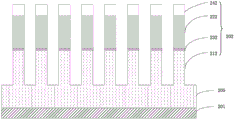
First, as shown in fig. 2A, a substrate structure is provided. The substrate structure includes a conductive layer 201 and a plurality of nano-pillars 202 spaced apart from each other over the conductive layer 201. Among them, the material of the conductive layer 201 may be an electrode material such as Al. Each of the nano-pillars 202 includes a first semiconductor layer 212 and a second semiconductor layer 222 on the first semiconductor layer 212. Here, the first semiconductor layer 212 and the second semiconductor layer 222 are different in conductivity type, so that a PN junction 232 may be formed at a contact interface of the first semiconductor layer 212 and the second semiconductor layer 222. In one embodiment, the material of the first semiconductor layer 212 and the material of the second semiconductor layer 222 may be the same, thereby forming a homojunction PN at the contact interface of the first semiconductor layer 212 and the second semiconductor layer 222. In another embodiment, the material of the first semiconductor layer 212 and the material of the second semiconductor layer 222 may also be different, so that a hetero PN junction is formed at a contact interface of the first semiconductor layer 212 and the second semiconductor layer 222. In addition, the substrate structure may further include a substrate (not shown), and the conductive layer 212 may be on the substrate.
Thereafter, as shown in fig. 2B, a graphene layer 203 is formed over the plurality of nanopillars 202, wherein the graphene layer 203 over each nanopillar 202 is in communication with each other. In one embodiment, the graphene layer may be formed on a metal substrate such as copper, platinum, tungsten, or nickel in advance; then, the graphene layer formed on the metal substrate is transferred onto the plurality of nanopillars. For example, a graphene layer may be deposited on a copper substrate by Chemical Vapor Deposition (CVD) or Plasma Enhanced Chemical Vapor Deposition (PECVD) at a temperature of 700-; and then transferring the graphene layer onto the nano-pillars by means of wet transfer. However, the present disclosure is not limited thereto, and the transfer of the graphene may be performed in other manners.
The structure of the resulting semiconductor device is described below with reference to fig. 2B.
As shown in fig. 2B, the semiconductor device includes: an electrically conductive layer 201, a plurality of nanopillars 202 spaced apart from one another over the electrically conductive layer 201, and a graphene layer 203 over the plurality of nanopillars 202, wherein the graphene layer 203 over each nanopillar 202 is in communication with one another. Each of the nano-pillars 202 includes a first semiconductor layer 212 and a second semiconductor layer 222 on the first semiconductor layer 212, the first semiconductor layer 212 and the second semiconductor layer 222 have different conductivity types, and a PN junction 232 may be formed at a contact interface of the first semiconductor layer 212 and the second semiconductor layer 222. In one embodiment, the lateral dimension of the nanopillars may be 5-5000 nm.
Thereafter, as shown in fig. 2C, a protective layer 204 may also be formed on the graphene layer 203 in the semiconductor device shown in fig. 2B. Preferably, the protective layer 204 may be a glass film; more preferably, the protective layer 204 may be a silica glass film.
Fig. 3A-3C illustrate various stages of a method of fabricating a semiconductor device according to another embodiment of the present disclosure. It should be noted that, since the manufacturing process of the semiconductor device has been described in detail with reference to fig. 2A to 2C, the present embodiment only focuses on the differences from the above embodiments, and reference may be made to the description of the above embodiments for relevant points.
First, as shown in fig. 3A, a substrate structure is provided. In contrast to the substrate structure shown in fig. 2A, each of the nano-pillars in the substrate structure shown in fig. 3A may further include an aluminum layer 242 on the second semiconductor layer 222. In addition, the substrate structure shown in fig. 3A may further include a third semiconductor layer 205 on the conductive layer 201, and the plurality of nano-pillars 202 are located on the third semiconductor layer 205. Here, the material of the third semiconductor layer 205 is the same as that of the first semiconductor layer 212, and is, for example, silicon. Note that since the material of the third semiconductor layer 205 is the same as that of the first semiconductor layer 212, fig. 3A integrally shows the third semiconductor layer 205 and the first semiconductor layer 212.
Then, as shown in fig. 3B, a graphene layer 203 is formed over the plurality of nanopillars 202, wherein the graphene layer 203 over each nanopillar 202 is in communication with each other. The graphene layer 203 may be formed according to the above-described manner, and will not be described in detail herein.
The structure of the resulting semiconductor device is described below with reference to fig. 3B.
As shown in fig. 3B, the semiconductor device includes: the semiconductor device includes an electrically conductive layer 201, a third semiconductor layer 205 on the electrically conductive layer 201, a plurality of nanopillars 202 spaced apart from each other on top of the third semiconductor layer 205, and a graphene layer 203 on top of the plurality of nanopillars 202, wherein the graphene layer 203 on top of each nanopillar 202 is in communication with each other, and a material of the third semiconductor layer 205 is the same as a material of the first semiconductor layer 212. Each of the nano-pillars 202 includes a first semiconductor layer 212, a second semiconductor layer 222 on the first semiconductor layer 212, and an aluminum layer 232 on the second semiconductor layer 222, the first semiconductor layer 212 and the second semiconductor layer 222 have different conductivity types, and a PN junction 232 is formed at a contact interface of the first semiconductor layer 212 and the second semiconductor layer 222.
Thereafter, as shown in fig. 3C, a protective layer 204, such as a glass film or the like, may also be formed on the graphene layer 203.
The substrate structures shown in fig. 2A and 3A may be formed according to different ways. One specific implementation of forming the substrate structure is described below in conjunction with fig. 4A-4E.
First, as shown in fig. 4A, an initial substrate structure is provided, which includes: a conductive layer 201, a first semiconductor layer 212 over the conductive layer 201, a second semiconductor layer 222 over the first semiconductor layer 212, and an aluminum layer 242 over the second semiconductor layer. The contact interface of the first semiconductor layer 212 and the second semiconductor layer 222 forms a PN junction 232.
Then, as shown in fig. 4B, an upper portion of the aluminum layer 242 is oxidized through an anodic oxidation process to form an aluminum oxide layer 401, wherein a plurality of nano holes 402 are formed in the aluminum oxide layer 401, and the nano holes 402 extend from an upper surface of the aluminum oxide layer 401 to a lower portion of the aluminum layer 242. It should be understood that "upper" and "lower" are merely relative concepts, i.e., the upper portion of the aluminum layer 242 is located relatively above the aluminum layer 242 with respect to the lower portion of the aluminum layer 242. In one embodiment, the lateral dimension (e.g., diameter) of the nanopore may be 5-5000nm, such as 10nm, 50nm, 100nm, 1000nm, 3000nm, and the like. In one embodiment, the above-described anodizing process may be performed using a neutral electrolyte including ammonium pentaborate and ammonium adipate and/or an acidic electrolyte including phosphoric acid and oxalic acid at a voltage of 0 to 100V. However, the present disclosure is not limited thereto. One skilled in the art can adjust the process conditions of the anodization process to obtain nanopores of different lateral dimensions in light of the teachings of the present disclosure.
It is noted that the "lateral dimension" of the nanopore/pillar herein refers to the dimension in the direction perpendicular to the direction in which the nanopore/pillar extends, e.g., the "lateral" refers to the horizontal direction if the nanopore extends vertically downward.
Next, as shown in fig. 4C, a hard mask 403 is filled in the plurality of nano holes 402. For example, a hard mask material such as titanium nitride may be deposited to fill the plurality of nanopores 402 and cover the aluminum oxide layer 401, after which the hard mask material may be planarized, e.g., Chemical Mechanical Polishing (CMP), to obtain a hard mask 403 having a surface substantially flush with the surface of the aluminum oxide layer 401.
Next, as shown in fig. 4D and 4E, the aluminum oxide layer 401, the lower portion of the aluminum layer 242, the second semiconductor layer 222, and at least a portion of the first semiconductor layer 212 are sequentially etched using the hard mask 403 as a mask. In one embodiment, the material of the first semiconductor layer 212 and the second semiconductor layer 222 may include silicon. First, the aluminum oxide layer 401 and the aluminum layer 242 may be etched using a Cl-containing plasma with the second semiconductor layer 222 as a stop layer, for example, BCl may be used3Obtaining a Cl-containing plasma as a source gas; then, at least a portion of the second semiconductor layer 222 and the first semiconductor layer 212 may be etched using the F-containing plasma.
In one implementation, as shown in fig. 4D, only a portion of the first semiconductor layer 212 may be etched away, that is, the first semiconductor layer 212 may stop in the first semiconductor layer 212 above the conductive layer 201 when etching the first semiconductor layer 212. The unetched portion 212A of the first semiconductor layer 212 serves as the third semiconductor layer 205 shown in fig. 3A, and the remaining portion 212B of the etched portion of the first semiconductor layer 212 and the second semiconductor layer 222 constitute the nanopillar 202 shown in fig. 3A.
In another implementation, as shown in fig. 4E, the first semiconductor layer 212 may be etched while stopping on the conductive layer 201.
After that, the hard mask 403 is removed, so that the substrate structure shown in fig. 3A can be formed. Preferably, after removing the hard mask 403, the surface of the aluminum layer 242 in the nanopillars may be cleaned to remove aluminum oxide of the surface of the aluminum layer. In one embodiment, the surface of the aluminum layer 242 in the nanopillars may be cleaned with a weakly alkaline cleaning agent, such as sodium carbonate or triethanolamine.
Thereafter, the aluminum layer 242 on the second semiconductor layer 222 may also be removed, thereby forming the substrate structure shown in fig. 2A.
So far, the semiconductor device and the manufacturing method thereof according to the embodiments of the present disclosure have been described in detail. Some details which are well known in the art have not been described in order to avoid obscuring the concepts of the present disclosure, and it will be fully apparent to those skilled in the art from the above description how to implement the techniques disclosed herein. In addition, the embodiments taught by the present disclosure can be freely combined. It will be appreciated by those skilled in the art that numerous modifications may be made to the embodiments described above without departing from the spirit and scope of the disclosure as defined by the appended claims.

Claims (19)

1. A method for manufacturing a semiconductor device, comprising:
providing a substrate structure, the substrate structure comprising:
a conductive layer; and
a plurality of nanopillars spaced apart from each other over the conductive layer, each nanopillar comprising a first semiconductor layer, a second semiconductor layer on the first semiconductor layer, and an aluminum layer on the second semiconductor layer, the first semiconductor layer being of a different conductivity type than the second semiconductor layer;
forming a graphene layer over the plurality of nanopillars, wherein the graphene layer over each nanopillar is in communication with each other;
wherein the step of providing a substrate structure comprises:
providing an initial substrate structure comprising:
a conductive layer;
a first semiconductor layer on the conductive layer;
a second semiconductor layer on the first semiconductor layer; and
an aluminum layer on the second semiconductor layer;
oxidizing an upper portion of the aluminum layer by an anodic oxidation process to form an aluminum oxide layer, wherein a plurality of nanopores are formed in the aluminum oxide layer, the nanopores extending from an upper surface of the aluminum oxide layer to a lower portion of the aluminum layer;
filling a hard mask in the plurality of nanopores;
etching the aluminum oxide layer, the lower part of the aluminum layer, the second semiconductor layer and at least one part of the first semiconductor layer in sequence by taking the hard mask as a mask;
removing the hard mask, thereby forming the plurality of nanopillars.
2. The method of claim 1, wherein the substrate structure further comprises a substrate, the conductive layer being on the substrate.
3. The method of claim 1, wherein the substrate structure further comprises:
a third semiconductor layer on the conductive layer, a material of the third semiconductor layer being the same as a material of the first semiconductor layer;
the plurality of nano-pillars is located over the third semiconductor layer.
4. The method of claim 1, wherein the material of the first semiconductor layer and the second semiconductor layer comprises silicon;
the etching the aluminum oxide layer, the lower portion of the aluminum layer, the second semiconductor layer, and at least a portion of the first semiconductor layer in sequence using the hard mask as a mask includes:
etching the aluminum oxide layer and the aluminum layer by using the second semiconductor layer as a stop layer and using Cl-containing plasma;
etching at least a portion of the second semiconductor layer and the first semiconductor layer using a plasma comprising F.
5. The method according to claim 1, wherein the anodizing process is performed at a voltage of 0-100V using a neutral electrolyte comprising ammonium pentaborate and ammonium adipate and/or an acidic electrolyte comprising phosphoric acid and oxalic acid.
6. The method of claim 1, further comprising:
and after removing the hard mask, cleaning the surface of the aluminum layer in the nano-pillar.
7. The method of claim 1, wherein forming a continuous graphene layer over the plurality of nanopillars comprises:
forming a graphene layer on a metal substrate in advance;
transferring the graphene layer formed on the metal substrate onto the plurality of nanopillars.
8. The method of claim 1, further comprising:
forming a protective layer on the graphene layer.
9. The method of claim 1, wherein the nanopore has a lateral dimension of 5-5000 nm.
10. The method of claim 1, wherein the nanopillars have a lateral dimension of 5-5000 nm.
11. The method of claim 1, wherein a material of the first semiconductor layer and a material of the second semiconductor layer are the same.
12. The method of claim 1, wherein a material of the first semiconductor layer and a material of the second semiconductor layer are different.
13. A semiconductor device, comprising:
a conductive layer;
a plurality of nanopillars spaced apart from each other over the conductive layer, each nanopillar comprising a first semiconductor layer, a second semiconductor layer on the first semiconductor layer, and an aluminum layer on the second semiconductor layer, the first semiconductor layer being of a different conductivity type than the second semiconductor layer; and
a graphene layer over the plurality of nanopillars, wherein the graphene layer over each nanopillar is in communication with each other;
wherein the second semiconductor layer is located on an upper surface of the first semiconductor layer and not on a side surface of the first semiconductor layer, and the aluminum layer is located on an upper surface of the second semiconductor layer and not on a side surface of the second semiconductor layer.
14. The apparatus of claim 13, further comprising:
a third semiconductor layer on the conductive layer, a material of the third semiconductor layer being the same as a material of the first semiconductor layer;
wherein the plurality of nanopillars is located over the third semiconductor layer.
15. The apparatus of claim 13, further comprising:
a substrate, the conductive layer being located on the substrate.
16. The apparatus of claim 13, further comprising:
a protective layer on the graphene layer.
17. The device of claim 13, wherein the nanopillars have a lateral dimension of 5-5000 nm.
18. The apparatus of claim 13, wherein a material of the first semiconductor layer and a material of the second semiconductor layer are the same.
19. The apparatus of claim 13, wherein a material of the first semiconductor layer and a material of the second semiconductor layer are different.
CN201610510623.2A 2016-07-01 2016-07-01 Semiconductor device and method for manufacturing the same Active CN107564980B (en)

Priority Applications (4)

Application Number Priority Date Filing Date Title
CN201610510623.2A CN107564980B (en) 2016-07-01 2016-07-01 Semiconductor device and method for manufacturing the same
US15/477,798 US11139405B2 (en) 2016-07-01 2017-04-03 Method for fabricating nanopillar solar cell using graphene
EP17178367.3A EP3264474A1 (en) 2016-07-01 2017-06-28 Method for fabricating nanopillar solar cell using graphene
US17/445,879 US20210391483A1 (en) 2016-07-01 2021-08-25 Nanopillar solar cell using graphene

Applications Claiming Priority (1)

Application Number Priority Date Filing Date Title
CN201610510623.2A CN107564980B (en) 2016-07-01 2016-07-01 Semiconductor device and method for manufacturing the same

Publications (2)

Publication Number Publication Date
CN107564980A CN107564980A (en) 2018-01-09
CN107564980B true CN107564980B (en) 2020-03-31

Family

ID=59253371

Family Applications (1)

Application Number Title Priority Date Filing Date
CN201610510623.2A Active CN107564980B (en) 2016-07-01 2016-07-01 Semiconductor device and method for manufacturing the same

Country Status (3)

Country Link
US (2) US11139405B2 (en)
EP (1) EP3264474A1 (en)
CN (1) CN107564980B (en)

Families Citing this family (3)

* Cited by examiner, † Cited by third party
Publication number Priority date Publication date Assignee Title
US11239415B2 (en) * 2019-04-18 2022-02-01 Nanya Technology Corporation Memory device and fabrication method thereof
CN112186055B (en) * 2020-09-29 2022-01-07 复旦大学 A combined solar energy three-dimensional integrated system and preparation method thereof
CN113948546A (en) * 2021-09-17 2022-01-18 国家电投集团科学技术研究院有限公司 Laminated battery and preparation method thereof

Citations (2)

* Cited by examiner, † Cited by third party
Publication number Priority date Publication date Assignee Title
CN103219413A (en) * 2013-04-10 2013-07-24 中国科学院微电子研究所 A kind of graphene radial heterojunction solar cell and preparation method thereof
CN103875080A (en) * 2011-08-19 2014-06-18 浦项工科大学校产学协力团 Solar cell and method for manufacturing same

Family Cites Families (16)

* Cited by examiner, † Cited by third party
Publication number Priority date Publication date Assignee Title
US5581091A (en) * 1994-12-01 1996-12-03 Moskovits; Martin Nanoelectric devices
JP4235440B2 (en) 2002-12-13 2009-03-11 キヤノン株式会社 Semiconductor device array and manufacturing method thereof
US20060207647A1 (en) 2005-03-16 2006-09-21 General Electric Company High efficiency inorganic nanorod-enhanced photovoltaic devices
JP2009506546A (en) 2005-08-24 2009-02-12 ザ トラスティーズ オブ ボストン カレッジ Apparatus and method for solar energy conversion using nanoscale co-metallic structures
JP5667748B2 (en) * 2009-03-18 2015-02-12 株式会社東芝 Light transmissive solar cell and method for manufacturing the same
US10164135B2 (en) * 2009-08-07 2018-12-25 Guardian Glass, LLC Electronic device including graphene-based layer(s), and/or method or making the same
US20130019924A1 (en) 2009-11-25 2013-01-24 The Trustees Of Boston College Nanoscopically Thin Photovoltaic Junction Solar Cells
US8513722B2 (en) * 2010-03-02 2013-08-20 Micron Technology, Inc. Floating body cell structures, devices including same, and methods for forming same
JP2012074569A (en) * 2010-09-29 2012-04-12 Jx Nippon Oil & Energy Corp Photoelectric conversion element
WO2012088481A2 (en) * 2010-12-22 2012-06-28 California Institute Of Technology Heterojunction microwire array semiconductor devices
WO2013062727A1 (en) * 2011-10-24 2013-05-02 Applied Materials, Inc. Method and apparatus of removing a passivation film and improving contact resistance in rear point contact solar cells
US20140251411A1 (en) * 2013-03-05 2014-09-11 Qualcomm Mems Technologies, Inc. Large area photovoltaic energy-collecting window/skylight
FR3005785B1 (en) * 2013-05-14 2016-11-25 Aledia OPTOELECTRONIC DEVICE AND METHOD FOR MANUFACTURING THE SAME
US9390923B2 (en) * 2014-07-03 2016-07-12 Applied Materials, Inc. Methods of removing residual polymers formed during a boron-doped amorphous carbon layer etch process
US9147875B1 (en) * 2014-09-10 2015-09-29 Cellink Corporation Interconnect for battery packs
JP6030176B2 (en) * 2015-03-19 2016-11-24 株式会社東芝 Photoelectric conversion element and manufacturing method thereof

Patent Citations (2)

* Cited by examiner, † Cited by third party
Publication number Priority date Publication date Assignee Title
CN103875080A (en) * 2011-08-19 2014-06-18 浦项工科大学校产学协力团 Solar cell and method for manufacturing same
CN103219413A (en) * 2013-04-10 2013-07-24 中国科学院微电子研究所 A kind of graphene radial heterojunction solar cell and preparation method thereof

Also Published As

Publication number Publication date
CN107564980A (en) 2018-01-09
EP3264474A1 (en) 2018-01-03
US11139405B2 (en) 2021-10-05
US20210391483A1 (en) 2021-12-16
US20180006169A1 (en) 2018-01-04

Similar Documents

Publication Publication Date Title
Huang et al. Ordered arrays of vertically aligned [110] silicon nanowires by suppressing the crystallographically preferred< 100> etching directions
Huang et al. Fabrication of silicon nanowires with precise diameter control using metal nanodot arrays as a hard mask blocking material in chemical etching
Togonal et al. Effect of wettability on the agglomeration of silicon nanowire arrays fabricated by metal-assisted chemical etching
JP5477752B2 (en) Method for forming a diode
US9051175B2 (en) Bulk nano-ribbon and/or nano-porous structures for thermoelectric devices and methods for making the same
US9337380B2 (en) Method for fabricating heterojunction interdigitated back contact photovoltaic cells
Weisse et al. Electroassisted transfer of vertical silicon wire arrays using a sacrificial porous silicon layer
US20210391483A1 (en) Nanopillar solar cell using graphene
TWI455342B (en) Solar cell with selective emitter structure and manufacturing method thereof
TW201520383A (en) Electropolishing and porosification
KR101353373B1 (en) A fabrication method of the vertically aligned silicon nano-structure used by metal-assisted chemical etching method, a vertically alligned silicon nano-structure fabricated by this method, and a device comprising the vertically alligned silicon nano-structure.
TWI619156B (en) Nanoscale heterostructure
CN101803038A (en) Thin film solar cell element and method for manufacturing same
CN102368503A (en) CNT (carbon nano tube)-silicon heterojunction solar cell and manufacturing method thereof
TWI643265B (en) Nano heterostructure and preparation method of nano transistor
CN108963003B (en) Solar cell
Gudovskikh et al. Impact of interface recombination on quantum efficiency of a‐Si: H/c‐Si solar cells based on Si wires
CN103746017B (en) A kind of solar cell and preparation method thereof
CN105513944A (en) Semiconductor device and production method thereof
CN102544136B (en) Nanomaterial electronic and photoelectronic device and manufacture method thereof
KR101355930B1 (en) Methods of manufacturing vertical silicon nano tubes using sidewall spacer technique and metal-assisted chemical etching process and vertical silicon nano tubes manufactured by the same
CN103715195B (en) Full annular grating CMOS structure based on silicon-based three-dimensional nano array and preparation method thereof
TWI503999B (en) Solar cell and manufacturing method thereof
TWI603488B (en) Method for preparing solar cell
KR101652402B1 (en) Solar cell having nanowire structure and method of fabricating the same

Legal Events

Date Code Title Description
PB01 Publication
PB01 Publication
SE01 Entry into force of request for substantive examination
GR01 Patent grant
GR01 Patent grant