CN107346084B - A kind of total reflection infrared reflection device and preparation method thereof - Google Patents
A kind of total reflection infrared reflection device and preparation method thereof Download PDFInfo
- Publication number
- CN107346084B CN107346084B CN201710605685.6A CN201710605685A CN107346084B CN 107346084 B CN107346084 B CN 107346084B CN 201710605685 A CN201710605685 A CN 201710605685A CN 107346084 B CN107346084 B CN 107346084B
- Authority
- CN
- China
- Prior art keywords
- liquid crystal
- light
- conductive substrates
- polymer network
- crystal layer
- Prior art date
- Legal status (The legal status is an assumption and is not a legal conclusion. Google has not performed a legal analysis and makes no representation as to the accuracy of the status listed.)
- Active
Links
- 238000002360 preparation method Methods 0.000 title claims abstract description 7
- 239000004973 liquid crystal related substance Substances 0.000 claims abstract description 130
- 239000000758 substrate Substances 0.000 claims abstract description 62
- 229920000642 polymer Polymers 0.000 claims abstract description 46
- 239000004986 Cholesteric liquid crystals (ChLC) Substances 0.000 claims abstract description 38
- 150000001768 cations Chemical class 0.000 claims abstract description 18
- 239000012535 impurity Substances 0.000 claims abstract description 14
- 230000005684 electric field Effects 0.000 claims abstract description 8
- 238000007789 sealing Methods 0.000 claims abstract description 8
- 239000000203 mixture Substances 0.000 claims description 34
- 239000002019 doping agent Substances 0.000 claims description 16
- 239000000178 monomer Substances 0.000 claims description 14
- 238000006116 polymerization reaction Methods 0.000 claims description 12
- 239000003112 inhibitor Substances 0.000 claims description 11
- 238000000576 coating method Methods 0.000 claims description 10
- IMNFDUFMRHMDMM-UHFFFAOYSA-N N-Heptane Chemical compound CCCCCCC IMNFDUFMRHMDMM-UHFFFAOYSA-N 0.000 claims description 9
- 230000005540 biological transmission Effects 0.000 claims description 9
- 239000011248 coating agent Substances 0.000 claims description 9
- 238000000034 method Methods 0.000 claims description 8
- VLKZOEOYAKHREP-UHFFFAOYSA-N n-Hexane Chemical compound CCCCCC VLKZOEOYAKHREP-UHFFFAOYSA-N 0.000 claims description 6
- 125000006850 spacer group Chemical group 0.000 claims description 6
- 238000004140 cleaning Methods 0.000 claims description 4
- 238000001035 drying Methods 0.000 claims description 4
- 239000002904 solvent Substances 0.000 claims description 4
- 230000033001 locomotion Effects 0.000 claims description 3
- 238000010438 heat treatment Methods 0.000 claims description 2
- 238000004519 manufacturing process Methods 0.000 claims 5
- 238000004806 packaging method and process Methods 0.000 claims 2
- 238000001816 cooling Methods 0.000 claims 1
- 230000001678 irradiating effect Effects 0.000 claims 1
- 230000000379 polymerizing effect Effects 0.000 claims 1
- 238000010345 tape casting Methods 0.000 claims 1
- 230000010287 polarization Effects 0.000 abstract description 2
- 239000010410 layer Substances 0.000 description 44
- 239000011295 pitch Substances 0.000 description 14
- LYCAIKOWRPUZTN-UHFFFAOYSA-N Ethylene glycol Chemical group OCCO LYCAIKOWRPUZTN-UHFFFAOYSA-N 0.000 description 6
- 239000000463 material Substances 0.000 description 6
- 210000002858 crystal cell Anatomy 0.000 description 5
- CURLTUGMZLYLDI-UHFFFAOYSA-N Carbon dioxide Chemical compound O=C=O CURLTUGMZLYLDI-UHFFFAOYSA-N 0.000 description 4
- 239000011521 glass Substances 0.000 description 4
- KWVGIHKZDCUPEU-UHFFFAOYSA-N 2,2-dimethoxy-2-phenylacetophenone Chemical compound C=1C=CC=CC=1C(OC)(OC)C(=O)C1=CC=CC=C1 KWVGIHKZDCUPEU-UHFFFAOYSA-N 0.000 description 2
- 229910002092 carbon dioxide Inorganic materials 0.000 description 2
- 239000001569 carbon dioxide Substances 0.000 description 2
- 125000004386 diacrylate group Chemical group 0.000 description 2
- 125000004185 ester group Chemical group 0.000 description 2
- NWVVVBRKAWDGAB-UHFFFAOYSA-N p-methoxyphenol Chemical compound COC1=CC=C(O)C=C1 NWVVVBRKAWDGAB-UHFFFAOYSA-N 0.000 description 2
- 230000003595 spectral effect Effects 0.000 description 2
- 238000004378 air conditioning Methods 0.000 description 1
- 230000009286 beneficial effect Effects 0.000 description 1
- 239000011247 coating layer Substances 0.000 description 1
- 230000007423 decrease Effects 0.000 description 1
- 230000000694 effects Effects 0.000 description 1
- 238000005516 engineering process Methods 0.000 description 1
- 239000003292 glue Substances 0.000 description 1
- 239000003999 initiator Substances 0.000 description 1
Images


Classifications
-
- G—PHYSICS
- G02—OPTICS
- G02F—OPTICAL DEVICES OR ARRANGEMENTS FOR THE CONTROL OF LIGHT BY MODIFICATION OF THE OPTICAL PROPERTIES OF THE MEDIA OF THE ELEMENTS INVOLVED THEREIN; NON-LINEAR OPTICS; FREQUENCY-CHANGING OF LIGHT; OPTICAL LOGIC ELEMENTS; OPTICAL ANALOGUE/DIGITAL CONVERTERS
- G02F1/00—Devices or arrangements for the control of the intensity, colour, phase, polarisation or direction of light arriving from an independent light source, e.g. switching, gating or modulating; Non-linear optics
- G02F1/01—Devices or arrangements for the control of the intensity, colour, phase, polarisation or direction of light arriving from an independent light source, e.g. switching, gating or modulating; Non-linear optics for the control of the intensity, phase, polarisation or colour
- G02F1/13—Devices or arrangements for the control of the intensity, colour, phase, polarisation or direction of light arriving from an independent light source, e.g. switching, gating or modulating; Non-linear optics for the control of the intensity, phase, polarisation or colour based on liquid crystals, e.g. single liquid crystal display cells
- G02F1/137—Devices or arrangements for the control of the intensity, colour, phase, polarisation or direction of light arriving from an independent light source, e.g. switching, gating or modulating; Non-linear optics for the control of the intensity, phase, polarisation or colour based on liquid crystals, e.g. single liquid crystal display cells characterised by the electro-optical or magneto-optical effect, e.g. field-induced phase transition, orientation effect, guest-host interaction or dynamic scattering
- G02F1/13718—Devices or arrangements for the control of the intensity, colour, phase, polarisation or direction of light arriving from an independent light source, e.g. switching, gating or modulating; Non-linear optics for the control of the intensity, phase, polarisation or colour based on liquid crystals, e.g. single liquid crystal display cells characterised by the electro-optical or magneto-optical effect, e.g. field-induced phase transition, orientation effect, guest-host interaction or dynamic scattering based on a change of the texture state of a cholesteric liquid crystal
-
- G—PHYSICS
- G02—OPTICS
- G02F—OPTICAL DEVICES OR ARRANGEMENTS FOR THE CONTROL OF LIGHT BY MODIFICATION OF THE OPTICAL PROPERTIES OF THE MEDIA OF THE ELEMENTS INVOLVED THEREIN; NON-LINEAR OPTICS; FREQUENCY-CHANGING OF LIGHT; OPTICAL LOGIC ELEMENTS; OPTICAL ANALOGUE/DIGITAL CONVERTERS
- G02F1/00—Devices or arrangements for the control of the intensity, colour, phase, polarisation or direction of light arriving from an independent light source, e.g. switching, gating or modulating; Non-linear optics
- G02F1/01—Devices or arrangements for the control of the intensity, colour, phase, polarisation or direction of light arriving from an independent light source, e.g. switching, gating or modulating; Non-linear optics for the control of the intensity, phase, polarisation or colour
- G02F1/13—Devices or arrangements for the control of the intensity, colour, phase, polarisation or direction of light arriving from an independent light source, e.g. switching, gating or modulating; Non-linear optics for the control of the intensity, phase, polarisation or colour based on liquid crystals, e.g. single liquid crystal display cells
- G02F1/133—Constructional arrangements; Operation of liquid crystal cells; Circuit arrangements
- G02F1/1333—Constructional arrangements; Manufacturing methods
- G02F1/1334—Constructional arrangements; Manufacturing methods based on polymer dispersed liquid crystals, e.g. microencapsulated liquid crystals
- G02F1/13345—Network or three-dimensional gels
Landscapes
- Physics & Mathematics (AREA)
- Nonlinear Science (AREA)
- Chemical & Material Sciences (AREA)
- Crystallography & Structural Chemistry (AREA)
- General Physics & Mathematics (AREA)
- Optics & Photonics (AREA)
- Dispersion Chemistry (AREA)
- Mathematical Physics (AREA)
- Liquid Crystal (AREA)
- Optical Filters (AREA)
Abstract
本发明公开了一种全反射红外反射器件及其制备方法,该器件包括相对设置的两块透光导电基板,两块所述透光导电基板封装形成密封腔,在密封腔内,两块透光导电基板相对的表面上分别覆有能反射左旋偏振光的液晶层一和能反射右旋偏振光的液晶层二,液晶层一中包含聚合物网络和具有左旋螺旋结构的胆甾相液晶,液晶层二中包含聚合物网络和具有右旋螺旋结构的胆甾相液晶,具有左旋螺旋结构的胆甾相液晶可用反射左旋偏振光,具有右旋螺旋结构的胆甾相液晶可以反射右旋偏振光,所以该器件能够对一定波段内红外全反射,聚合物网络能够捕获所述液晶层一或所述液晶层二中的杂质阳离子,在电场下,聚合物网络带动胆甾相液晶移动,实现反射波段调节。

The invention discloses a total reflection infrared reflection device and a preparation method thereof. The device comprises two light-transmitting conductive substrates arranged opposite to each other. The two light-transmitting conductive substrates are packaged to form a sealing cavity. The opposite surfaces of the photoconductive substrate are respectively covered with a liquid crystal layer one capable of reflecting left-handed polarized light and a liquid crystal layer two capable of reflecting right-handed polarized light. The second liquid crystal layer contains a polymer network and a cholesteric liquid crystal with a right-handed helical structure. The cholesteric liquid crystal with a left-handed helical structure can reflect left-handed polarized light, and the cholesteric liquid crystal with a right-handed helical structure can reflect right-handed polarization. Therefore, the device can totally reflect infrared rays in a certain band, and the polymer network can capture the impurity cations in the liquid crystal layer 1 or the liquid crystal layer 2. Under the electric field, the polymer network drives the cholesteric liquid crystal to move, realizing Reflection band adjustment.
Description
技术领域technical field
本发明涉及建筑家具生活领域,特别是一种基于电响应的全反射红外反射器件及其制备方法。The invention relates to the living field of building furniture, in particular to a total reflection infrared reflection device based on electrical response and a preparation method thereof.
背景技术Background technique
建筑的内部环境和人的健康有着非常密切的关系,尤其是建筑内部温度对人有着非常大的影响,于是人们利用空调、暖气等设备来调节建筑内部的温度,使其在一个合适的范围。但是这些设备的使用会增加二氧化碳的排放量,并且会对环境产生非常不利的影响。The internal environment of a building has a very close relationship with people's health, especially the internal temperature of the building has a great impact on people, so people use air conditioning, heating and other equipment to adjust the temperature inside the building to make it within a suitable range. But the use of these devices increases carbon dioxide emissions and has a very negative impact on the environment.
于是建筑外壳技术开始发挥重大的作用,无机涂料等大量创新方法得到应用。但阳光中的红外线可以透过窗户进入室内,影响室内环境温度。As a result, building shell technology began to play a major role, and a large number of innovative methods such as inorganic coatings were applied. However, the infrared rays in sunlight can enter the room through the window and affect the indoor ambient temperature.
于是人们开始关注窗户的设计,希望其能控制对太阳光的透过和反射,来达到人们想要的舒适的室内环境。人们尝试使用百叶窗、液晶玻璃、镀膜玻璃等,但这些措施无法在调节对红外线的同时又不影响可见光的透过。人们发现基于聚合物网络稳定胆甾相液晶的红外反射片可以调节红外线的透过和反射,同时又不影响可见光。通过电压调节红外反射片,使其在低温时透过红外线,高温时反射红外线。该红外反射片可以调节建筑内部温度,可在一定程度上代替空调等温度调节设备的作用,解决了镀膜玻璃的局限性,有利于减少二氧化碳的排放,有利于保护环境,同时可以在汽车玻璃方面得到应用。Therefore, people began to pay attention to the design of windows, hoping that it can control the transmission and reflection of sunlight to achieve the comfortable indoor environment that people want. People try to use blinds, liquid crystal glass, coated glass, etc., but these measures cannot adjust the infrared rays without affecting the transmission of visible light. It has been found that infrared reflective sheets based on polymer network stabilized cholesteric liquid crystals can adjust the transmission and reflection of infrared rays without affecting visible light. The infrared reflector is adjusted by voltage so that it transmits infrared rays at low temperature and reflects infrared rays at high temperature. The infrared reflector can adjust the internal temperature of the building, can replace the role of temperature adjustment equipment such as air conditioners to a certain extent, solve the limitations of coated glass, help reduce carbon dioxide emissions, and protect the environment, and can be used in automotive glass. get applied.
太阳光中的红外线分为左旋偏振光和右旋偏振光,胆甾相液晶的螺旋结构也分为左旋和右旋,螺旋结构左旋的胆甾相液晶只能反射左旋偏振光,螺旋结构右旋的胆甾相液晶只能反射右旋偏振光,所以只含有一种螺旋结构的胆甾相液晶的红外反射片只能反射一种偏振光,无法做到对左旋偏振光和右旋偏振光的全反射。限制了红外反射片的应用。Infrared rays in sunlight are divided into left-handed polarized light and right-handed polarized light, and the helical structure of cholesteric liquid crystal is also divided into left-handed and right-handed. The cholesteric liquid crystal can only reflect right-handed polarized light, so the infrared reflective sheet of cholesteric liquid crystal containing only one kind of helical structure can only reflect one kind of polarized light, and cannot achieve the effect of left-handed polarized light and right-handed polarized light. Total reflection. The application of infrared reflector is limited.
发明内容SUMMARY OF THE INVENTION
本发明所要解决的技术问题是提供一种新型的全反射红外反射器件及其制备方法。The technical problem to be solved by the present invention is to provide a novel total reflection infrared reflection device and a preparation method thereof.
本发明所采取的技术方案是:The technical scheme adopted by the present invention is:
一种全反射红外反射器件,包括相对设置的两块透光导电基板,两块所述透光导电基板封装形成密封腔,在所述密封腔内,两块所述透光导电基板相对的表面上分别覆有能反射左旋偏振光的液晶层一和能反射右旋偏振光的液晶层二,所述液晶层一中包含聚合物网络和具有左旋螺旋结构的胆甾相液晶,所述液晶层二中包含聚合物网络和具有右旋螺旋结构的胆甾相液晶,所述聚合物网络能够捕获所述液晶层一或所述液晶层二中的杂质阳离子,在电场下,所述杂质阳离子运动带动所述聚合物网络移动,所述聚合物网络带动所述胆甾相液晶移动,使得所述胆甾相液晶的螺距发生改变。A total reflection infrared reflection device, comprising two light-transmitting conductive substrates arranged oppositely, the two light-transmitting conductive substrates are encapsulated to form a sealing cavity, and in the sealing cavity, the opposite surfaces of the two light-transmitting conductive substrates A
在一些优选的实施方式中,两块所述透光导电基板相对的表面上均覆有平行配向层,所述液晶层一和所述液晶层二覆于所述平行配向层上。In some preferred embodiments, the opposite surfaces of the two light-transmitting conductive substrates are covered with parallel alignment layers, and the first liquid crystal layer and the second liquid crystal layer are covered on the parallel alignment layers.
在一些优选的实施方式中,所述密封腔内还设有用于控制所述密封腔高度的间隔子。In some preferred embodiments, spacers for controlling the height of the sealed cavity are further provided in the sealed cavity.
在一些优选的实施方式中,所述液晶层一和所述液晶层二的厚度为10-50μm。In some preferred embodiments, the thickness of the first liquid crystal layer and the second liquid crystal layer is 10-50 μm.
本发明还提供了一种如上所述的全反射红外反射器件的制备方法,包括以下步骤:The present invention also provides a preparation method of the above-mentioned total reflection infrared reflection device, comprising the following steps:
制备或取两块透光导电基板;Prepare or take two transparent conductive substrates;
在两块所述透光导电基板的一面上制备平行配向层;preparing parallel alignment layers on one side of the two light-transmitting conductive substrates;
配制液晶混合物一和液晶混合物二,所述液晶混合物一中含有负性液晶、液晶单体、左旋手性掺杂剂、光引发剂和阻聚剂,所述液晶混合物二中含有负性液晶、液晶单体、右旋手性掺杂剂、光引发剂和阻聚剂;Liquid crystal mixture one and liquid crystal mixture two are prepared, the liquid crystal mixture one contains negative liquid crystal, liquid crystal monomer, left-handed chiral dopant, photoinitiator and polymerization inhibitor, Liquid crystal monomers, right-handed chiral dopants, photoinitiators and polymerization inhibitors;
分别将所述液晶混合物一和所述液晶混合物二涂覆到两块所述透光导电基板的平行配向层上,紫外光照射所述液晶混合物一和所述液晶混合物二,所述液晶单体发生聚合,形成聚合物网络;The liquid crystal mixture one and the liquid crystal mixture two are respectively coated on the parallel alignment layers of the two light-transmitting conductive substrates, and the liquid crystal mixture one and the liquid crystal mixture two are irradiated with ultraviolet light. Polymerization occurs to form a polymer network;
清洗两块所述透光导电基板,去除所述左旋手性掺杂剂、所述右旋手性掺杂剂、所述光引发剂、所述阻聚剂、所述负性液晶和未发生聚合的所述单体,干燥;Cleaning two of the light-transmitting conductive substrates to remove the left-handed chiral dopant, the right-handed chiral dopant, the photoinitiator, the polymerization inhibitor, the negative liquid crystal and the the polymerized monomer, dried;
将两块所述透光导电基板覆有所述聚合物网络的一面相对设置,并将其封装形成液晶盒;The sides of the two transparent conductive substrates covered with the polymer network are arranged opposite to each other, and they are packaged to form a liquid crystal cell;
向所述液晶盒内填充负性液晶。The liquid crystal cell is filled with negative liquid crystal.
在一些优选的实施方式中,将所述液晶混合物一和所述液晶混合物二涂覆到两块所述透光导电基板的平行配向层上是采用刮涂、棒涂中的任一种工艺。In some preferred embodiments, the coating of the
在一些优选的实施方式中,涂覆到两块所述透光导电基板的平行配向层上的所述液晶混合物一和所述液晶混合物二的厚度为10-50μm。In some preferred embodiments, the thickness of the
在一些优选的实施方式中,所述干燥的温度为70-90℃。In some preferred embodiments, the drying temperature is 70-90°C.
在一些优选的实施方式中,清洗两块所述透光导电基板是采用正己烷、正庚烷中的至少一种溶剂进行清洗。In some preferred embodiments, cleaning the two light-transmitting conductive substrates is performed by using at least one solvent selected from n-hexane and n-heptane.
在一些优选的实施方式中,将两块所述透光导电基板覆有所述聚合物网络的一面相对设置后还包括在两块所述透光导电基板之间设置间隔子的步骤。In some preferred embodiments, the step of arranging spacers between the two light-transmitting conductive substrates after the surfaces of the two light-transmitting conductive substrates covered with the polymer network are disposed opposite to each other.
本发明的有益效果是:The beneficial effects of the present invention are:
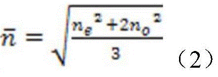
本发明提供了一种全反射红外反射器件及其制备方法,该器件包括相对设置的两块透光导电基板,两块所述透光导电基板封装形成密封腔,在密封腔内,两块透光导电基板相对的表面上分别覆有能反射左旋偏振光的液晶层一和能反射右旋偏振光的液晶层二,液晶层一中包含聚合物网络和具有左旋螺旋结构的胆甾相液晶,液晶层二中包含聚合物网络和具有右旋螺旋结构的胆甾相液晶,具有左旋螺旋结构的胆甾相液晶可用反射左旋偏振光,具有右旋螺旋结构的胆甾相液晶可以反射右旋偏振光,所以该器件能够对一定波段内左旋偏振光和右旋偏振光实现全反射,所述聚合物网络能够捕获所述液晶层一或所述液晶层二中的杂质阳离子,只要在透光导电基板上施加电压,即可将液晶层一和液晶层二置于电场下,杂质阳离子在电场下会向与电源负极相连的透光导电基板运动,杂质阳离子运动带动所述聚合物网络移动,所述聚合物网络带动所述胆甾相液晶移动,使得所述胆甾相液晶的螺距发生改变。在通电状态下,密封腔中中,聚合物网络因捕获阳离子向负极运动,所述胆甾相液晶分散在所述聚合物网络中,所述胆甾相液晶在聚合物网络的带动下,向负极运动,使得靠近与电源负极相连的透光导电基板的液晶螺距减小,靠近与电源正极相连的透光导电基板的液晶螺距增大,总体在密封腔内形成具有一定螺距梯度的螺旋结构。根据以下公式: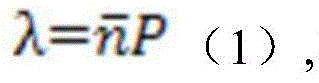


综上所述,本发明提供了一种红外反射器件,既能够实现某一波段的红外全反射,又能够实现反射波段调节。To sum up, the present invention provides an infrared reflection device, which can not only realize the total infrared reflection of a certain wavelength band, but also realize the adjustment of the reflection wavelength band.
附图说明Description of drawings
图1为全反射红外反射器件的截面图。FIG. 1 is a cross-sectional view of a total reflection infrared reflection device.
图2为未通电状态下全反射红外反射器件的局部截面图。FIG. 2 is a partial cross-sectional view of the total reflection infrared reflection device in an unpowered state.
图3为通电状态下全反射红外反射器件的局部截面图。FIG. 3 is a partial cross-sectional view of the total reflection infrared reflecting device in a power-on state.
具体实施方式Detailed ways
实施例1:Example 1:
根据下述步骤制备全反射红外反射器件:The total reflection infrared reflecting device was prepared according to the following steps:
首先制备两块透光导电基板,每块所述透光导电基板均包括基板和导电层;在两块所述透光导电基板的一面上制备平行配向层;First, two light-transmitting conductive substrates are prepared, and each of the light-transmitting conductive substrates includes a substrate and a conductive layer; a parallel alignment layer is prepared on one side of the two light-transmitting conductive substrates;
在黄光条件下,按照负性液晶:液晶单体:左旋手性掺杂剂:光引发剂:阻聚剂的质量比为81.2:12.6:5:1:0.2的比例,称取各材料至棕色瓶中,其中,负性液晶选用德国默克公司的MLC-2079,液晶单体选用飞利浦研究实验室的ethylene glycol twin diacrylate,左旋手性掺杂剂选用德国默克公司的S811,光引发剂选用TCI公司的Irgacure-651,阻聚剂选用对羟基苯甲醚,混合均匀,得到液晶混合物一;Under the condition of yellow light, according to the mass ratio of negative liquid crystal: liquid crystal monomer: left-handed chiral dopant: photoinitiator: polymerization inhibitor 81.2:12.6:5:1:0.2, weigh each material to In the brown bottle, the negative liquid crystal is MLC-2079 from Merck, Germany, the liquid crystal monomer is ethylene glycol twin diacrylate from Philips Research Laboratory, the left-handed chiral dopant is S811 from Merck, Germany, and the photoinitiator is S811. Select Irgacure-651 from TCI company, select p-hydroxyanisole as the polymerization inhibitor, mix well, and obtain
在黄光条件下,按照负性液晶:液晶单体:右旋手性掺杂剂:光引发剂:阻聚剂的质量比为81.2:12.6:5:1:0.2的比例,称取各材料至棕色瓶中,其中,负性液晶选用德国默克公司的MLC-2079,液晶单体选用飞利浦研究实验室的ethylene glycol twin diacrylate,右旋手性掺杂剂选用德国默克公司的R811,光引发剂选用TCI公司的Irgacure-651,阻聚剂选用对羟基苯甲醚,混合均匀,得到液晶混合物二;Under the condition of yellow light, according to the ratio of negative liquid crystal: liquid crystal monomer: right-handed chiral dopant: photoinitiator: polymerization inhibitor, the mass ratio is 81.2:12.6:5:1:0.2, weigh each material. In a brown bottle, the negative liquid crystal was MLC-2079 from Merck, Germany, the liquid crystal monomer was ethylene glycol twin diacrylate from Philips Research Laboratory, and the right-handed chiral dopant was R811 from Merck, Germany. The initiator selects Irgacure-651 of TCI Company, and the polymerization inhibitor selects p-hydroxyanisole, and mixes uniformly to obtain liquid crystal mixture II;
将所述液晶混合物一和所述液晶混合物二加热至70℃,然后分别将所述液晶混合物一和所述液晶混合物二涂覆到两块所述透光导电基板的平行配向层上,涂覆工艺为刮涂、棒涂中的任一种工艺,涂覆层的厚度为10-50μm,涂覆完成后,降温至室温,保温30min,使液晶分子取向;然后紫外光照射所述液晶混合物一和所述液晶混合物二,所述液晶单体发生聚合,形成聚合物网络,选用的液晶单体带有能够捕获阳离子的酯基,所以形成的聚合物网络也带有酯基,也能够捕获阳离子;The
采用正己烷、正庚烷中的至少一种溶剂清洗两块所述透光导电基板,去除所述左旋手性掺杂剂、所述右旋手性掺杂剂、所述光引发剂、所述阻聚剂、所述负性液晶和未发生聚合的所述单体,放入烘箱中70-90℃干燥两小时,去除溶剂;Use at least one solvent in n-hexane and n-heptane to clean the two light-transmitting conductive substrates to remove the left-handed chiral dopant, the right-handed chiral dopant, the photoinitiator, the The polymerization inhibitor, the negative liquid crystal and the unpolymerized monomer are put into an oven for drying at 70-90° C. for two hours to remove the solvent;
将两块所述透光导电基板覆有所述聚合物网络的一面相对设置,在两块所述透光导电基板之间设置间隔子,用于支撑器件的厚度,然后利用紫外胶紫外固化将两块所述透光导电基板封装形成液晶盒;The two transparent conductive substrates covered with the polymer network are arranged opposite each other, and a spacer is arranged between the two transparent conductive substrates to support the thickness of the device, and then UV glue is used to cure the polymer network. Two pieces of the light-transmitting conductive substrates are packaged to form a liquid crystal cell;
向所述液晶盒内填充负性液晶,负性液晶选用德国默克公司的MLC-2079,由于两块透光导电基板上覆有的聚合物网络是分别在左旋掺杂剂和右旋掺杂剂的作用下形成的,所以向液晶盒中填充负性液晶,负性液晶分散于聚合物网络中,在聚合物网络和平行配向层的共同作用下,分别在两块透光导电基板表面形成一个具有左旋螺旋结构的胆甾相液晶和一个具有右旋螺旋结构的胆甾相液晶。The liquid crystal cell is filled with negative liquid crystal, and the negative liquid crystal is MLC-2079 from Merck, Germany, because the polymer network covered on the two light-transmitting conductive substrates is respectively doped with left-handed dopant and right-handed dopant. Therefore, the negative liquid crystal is filled into the liquid crystal cell, and the negative liquid crystal is dispersed in the polymer network. A cholesteric liquid crystal with a left-handed helical structure and a cholesteric liquid crystal with a right-handed helical structure.
制备得到的全反射红外反射器件的截面图如图1所示,该全反射红外反射器件,包括相对设置的两块透光导电基板,每块所述透光导电基板均包括基板1和导电层2,两块所述透光导电基板相对的表面上即导电层2上均覆有平行配向层3,两块所述透光导电基板封装形成密封腔4,在所述密封腔4内,两块所述透光导电基板相对的表面上分别覆有能反射左旋偏振光的液晶层一5和能反射右旋偏振光的液晶层二6,所述液晶层一5和所述液晶层二6覆于所述平行配向层3上。所述液晶层一5和所述液晶层二6的厚度为10-50μm。所述密封腔4内还设有用于控制所述密封腔4高度的间隔子12。The cross-sectional view of the prepared total reflection infrared reflection device is shown in Figure 1. The total reflection infrared reflection device includes two light-transmitting conductive substrates arranged opposite each other, and each of the light-transmitting conductive substrates includes a
参照图2,图2为未通电状态下全反射红外反射器件的局部截面图,所述液晶层一5中包含聚合物网络7和具有左旋螺旋结构的胆甾相液晶8,所述液晶层二6中包含聚合物网络9和具有右旋螺旋结构的胆甾相液晶10。具有左旋螺旋结构的胆甾相液晶8可用反射左旋偏振光,具有右旋螺旋结构的胆甾相液晶10可以反射右旋偏振光,所以该器件能够对一定波段内左旋偏振光和右旋偏振光实现全反射。所述聚合物网络7和9能够捕获所述液晶层一5或所述液晶层二6中的杂质阳离子11。Referring to FIG. 2, FIG. 2 is a partial cross-sectional view of a total reflection infrared reflective device in an unpowered state, the liquid crystal layer one 5 includes a
参照图3,图3为通电状态下全反射红外反射器件的局部截面图,所述聚合物网络7和9能够捕获所述液晶层一5或所述液晶层二6中的杂质阳离子,只要在透光导电基板上施加电压,即可将液晶层一5和液晶层二6置于电场下,杂质阳离子11在电场下会向与电源负极相连的透光导电基板运动,杂质阳离子11运动带动所述聚合物网络移动,所述聚合物网络7和9带动所述胆甾相液晶8和10移动,使得所述胆甾相液晶8和10的螺距发生改变。在通电状态下,密封腔中中,聚合物网络7和9因捕获阳离子11向负极运动,所述胆甾相液晶8和10分散在所述聚合物网络7和9中,所述胆甾相液晶8和10在聚合物网络7和9的带动下,向负极运动,使得靠近与电源负极相连的透光导电基板的液晶螺距减小,靠近与电源正极相连的透光导电基板的液晶螺距增大,总体在密封腔内形成具有一定螺距梯度的螺旋结构。根据以下公式:


Claims (9)
Priority Applications (3)
| Application Number | Priority Date | Filing Date | Title |
|---|---|---|---|
| CN201710605685.6A CN107346084B (en) | 2017-07-21 | 2017-07-21 | A kind of total reflection infrared reflection device and preparation method thereof |
| US16/491,490 US11143902B2 (en) | 2017-07-21 | 2017-11-15 | Total-reflection infrared reflection device and preparation method thereof |
| PCT/CN2017/110992 WO2019015181A1 (en) | 2017-07-21 | 2017-11-15 | Total-reflection infrared reflective device and preparation method thereof |
Applications Claiming Priority (1)
| Application Number | Priority Date | Filing Date | Title |
|---|---|---|---|
| CN201710605685.6A CN107346084B (en) | 2017-07-21 | 2017-07-21 | A kind of total reflection infrared reflection device and preparation method thereof |
Publications (2)
| Publication Number | Publication Date |
|---|---|
| CN107346084A CN107346084A (en) | 2017-11-14 |
| CN107346084B true CN107346084B (en) | 2020-10-16 |
Family
ID=60257001
Family Applications (1)
| Application Number | Title | Priority Date | Filing Date |
|---|---|---|---|
| CN201710605685.6A Active CN107346084B (en) | 2017-07-21 | 2017-07-21 | A kind of total reflection infrared reflection device and preparation method thereof |
Country Status (3)
| Country | Link |
|---|---|
| US (1) | US11143902B2 (en) |
| CN (1) | CN107346084B (en) |
| WO (1) | WO2019015181A1 (en) |
Families Citing this family (16)
| Publication number | Priority date | Publication date | Assignee | Title |
|---|---|---|---|---|
| CN107346084B (en) * | 2017-07-21 | 2020-10-16 | 华南师范大学 | A kind of total reflection infrared reflection device and preparation method thereof |
| CN107991814B (en) * | 2017-12-25 | 2021-04-30 | Tcl华星光电技术有限公司 | Liquid crystal display panel and preparation method thereof |
| CN108663867A (en) * | 2018-04-11 | 2018-10-16 | 华南师范大学 | A kind of laser protective film of dyestuff doping |
| CN108761945B (en) * | 2018-04-18 | 2021-05-14 | 深圳市国华光电科技有限公司 | An electrically responsive liquid crystal dimming device |
| CN108415204B (en) * | 2018-04-28 | 2024-02-13 | 华南师范大学 | A multi-stable electrically responsive smart window and its preparation method |
| CN108803182B (en) * | 2018-05-25 | 2020-06-16 | 华南师范大学 | Laser protective film and laser protective equipment comprising same |
| CN108845462B (en) * | 2018-06-29 | 2022-05-24 | 南方科技大学 | An all-solid-state reflective/absorbing film and its preparation method and application |
| CN109001930B (en) * | 2018-07-13 | 2021-11-02 | 华南师范大学 | A kind of electric response infrared reflection device and preparation method thereof |
| CN109298564B (en) * | 2018-11-09 | 2022-02-08 | 京东方科技集团股份有限公司 | Display device |
| CN111812904B (en) * | 2020-07-15 | 2022-08-16 | 深圳市国华光电科技有限公司 | Liquid crystal multilayer film and preparation method thereof |
| CN113534554A (en) * | 2021-07-06 | 2021-10-22 | 北京科技大学 | A kind of preparation method of liquid crystal thin film material with adjustable total reflection waveband |
| CN113777841B (en) * | 2021-08-13 | 2024-04-19 | 华南师范大学 | Reflector and preparation method and application thereof |
| CN114690479B (en) * | 2022-04-14 | 2024-04-30 | 南京大学 | Liquid crystal geometric phase device and preparation method and detection device thereof |
| CN116224667B (en) * | 2023-02-22 | 2025-08-22 | 南京大学 | Adjustable liquid crystal holographic device and preparation method thereof, and holographic light field modulation device |
| CN116859645A (en) * | 2023-06-01 | 2023-10-10 | 重庆汉朗精工科技有限公司 | Electric control low-radiation glass |
| CN119200287B (en) * | 2024-09-02 | 2025-12-09 | 南京大学 | Liquid crystal image identifier, preparation method thereof and image identification device |
Citations (6)
| Publication number | Priority date | Publication date | Assignee | Title |
|---|---|---|---|---|
| US5691795A (en) * | 1991-05-02 | 1997-11-25 | Kent State University | Polymer stabilized liquid crystalline light modulating device and material |
| CN102640022A (en) * | 2009-12-25 | 2012-08-15 | 大日本印刷株式会社 | infrared reflective member |
| CN102749669A (en) * | 2012-06-20 | 2012-10-24 | 京东方科技集团股份有限公司 | Reflecting polaroid, method for producing same and liquid crystal display device |
| CN104662453A (en) * | 2012-09-28 | 2015-05-27 | 富士胶片株式会社 | Infrared-blocking film, infrared-blocking laminated glass, and infrared-blocking member |
| CN106646985A (en) * | 2016-11-16 | 2017-05-10 | 深圳市国华光电科技有限公司 | Waveband tunable infrared reflector and production method thereof |
| CN106646986A (en) * | 2017-02-10 | 2017-05-10 | 华南师范大学 | Electric response infrared reflection device and preparation method thereof |
Family Cites Families (12)
| Publication number | Priority date | Publication date | Assignee | Title |
|---|---|---|---|---|
| EP0582656B1 (en) | 1991-05-02 | 1999-04-07 | Kent State University | Crystalline light modulating device and material |
| ATE179259T1 (en) | 1992-05-18 | 1999-05-15 | Univ Kent State Ohio | LIQUID CRYSTALLINE LIGHT MODULATING DEVICE AND MATERIAL |
| JP3139486B2 (en) * | 1999-01-27 | 2001-02-26 | 日本電気株式会社 | Liquid crystal light modulation element, color filter using the same, and display device |
| US6704073B2 (en) * | 2002-03-12 | 2004-03-09 | Eastman Kodak Company | Method of coating a polymer-dispersed electro-optical fluid and sheets formed thereby |
| US7238397B2 (en) * | 2004-12-03 | 2007-07-03 | Xerox Corporation | Black/white cholesteric bistable display with increased white reflectivity |
| JP5020289B2 (en) * | 2009-06-11 | 2012-09-05 | 富士フイルム株式会社 | Infrared light reflector and infrared light reflective laminated glass |
| US20160103351A1 (en) * | 2013-05-30 | 2016-04-14 | Kent State University | Fast electrooptic switching devices employing polymer template shaped by blue phase liquid crystal |
| KR102097818B1 (en) * | 2015-07-01 | 2020-04-07 | 주식회사 엘지화학 | Substrate film |
| CN105676489B (en) | 2015-12-17 | 2019-08-27 | 深圳市国华光电科技有限公司 | An Infrared Reflective Device Based on Electrical Response |
| KR102835164B1 (en) * | 2016-11-30 | 2025-07-21 | 엘지디스플레이 주식회사 | Mirror cell and display device comprising the same |
| CN106646951A (en) * | 2017-01-09 | 2017-05-10 | 南方科技大学 | Reflecting film and preparation method thereof |
| CN107346084B (en) * | 2017-07-21 | 2020-10-16 | 华南师范大学 | A kind of total reflection infrared reflection device and preparation method thereof |
-
2017
- 2017-07-21 CN CN201710605685.6A patent/CN107346084B/en active Active
- 2017-11-15 WO PCT/CN2017/110992 patent/WO2019015181A1/en not_active Ceased
- 2017-11-15 US US16/491,490 patent/US11143902B2/en active Active
Patent Citations (6)
| Publication number | Priority date | Publication date | Assignee | Title |
|---|---|---|---|---|
| US5691795A (en) * | 1991-05-02 | 1997-11-25 | Kent State University | Polymer stabilized liquid crystalline light modulating device and material |
| CN102640022A (en) * | 2009-12-25 | 2012-08-15 | 大日本印刷株式会社 | infrared reflective member |
| CN102749669A (en) * | 2012-06-20 | 2012-10-24 | 京东方科技集团股份有限公司 | Reflecting polaroid, method for producing same and liquid crystal display device |
| CN104662453A (en) * | 2012-09-28 | 2015-05-27 | 富士胶片株式会社 | Infrared-blocking film, infrared-blocking laminated glass, and infrared-blocking member |
| CN106646985A (en) * | 2016-11-16 | 2017-05-10 | 深圳市国华光电科技有限公司 | Waveband tunable infrared reflector and production method thereof |
| CN106646986A (en) * | 2017-02-10 | 2017-05-10 | 华南师范大学 | Electric response infrared reflection device and preparation method thereof |
Also Published As
| Publication number | Publication date |
|---|---|
| US20200041827A1 (en) | 2020-02-06 |
| WO2019015181A1 (en) | 2019-01-24 |
| CN107346084A (en) | 2017-11-14 |
| US11143902B2 (en) | 2021-10-12 |
Similar Documents
| Publication | Publication Date | Title |
|---|---|---|
| CN107346084B (en) | A kind of total reflection infrared reflection device and preparation method thereof | |
| CN106646985B (en) | Infrared reflecting device with tunable wave band and preparation method thereof | |
| CN105676489B (en) | An Infrared Reflective Device Based on Electrical Response | |
| CN104793381B (en) | A kind of electroresponse infrared external reflection window and infrared light reflection method | |
| CN116009298B (en) | Liquid crystal dimming device | |
| CN109917594B (en) | A kind of privacy protection infrared reflection smart window and preparation method thereof | |
| CN103890643B (en) | Switching elements containing liquid crystal media | |
| CN108761945B (en) | An electrically responsive liquid crystal dimming device | |
| CN106646986A (en) | Electric response infrared reflection device and preparation method thereof | |
| CN113311625A (en) | Polymer stabilized cholesteric liquid crystal color-changing glass and preparation method and application thereof | |
| CN106997133A (en) | A kind of preparation method of infrared external reflection device | |
| CN106019754A (en) | Thermal-response infrared total reflection device and preparing method thereof | |
| CN108803182B (en) | Laser protective film and laser protective equipment comprising same | |
| CN110703470B (en) | A dual-response dimming device and its preparation method, dimming method and optical device | |
| Ranjkesh et al. | Ultrathin, transparent, thermally-insulated, and energy-efficient flexible window using coatable chiral-nematic liquid crystal polymer | |
| WO2018227870A1 (en) | Infrared reflection device with adjustable reflection proportion | |
| CN113391492B (en) | A kind of near-infrared light shielding film material, preparation method and application | |
| Du et al. | Anti‐UV Passive Radiative Cooling Chiral Nematic Liquid Crystal Films for Thermal Management | |
| CN109085712B (en) | Temperature response type liquid crystal material, light regulator and manufacturing method thereof | |
| CN108319059B (en) | An Electrically Responsive Infrared Reflecting Device | |
| Sen et al. | Polymer Dispersed Liquid Crystal Smart Film Technologies: Overview | |
| Li et al. | Reflective cholesteric liquid crystal polarizers and their applications | |
| CN113589573B (en) | An intelligent liquid crystal dimming film that senses changes in ambient light | |
| CN109143623B (en) | Infrared reflection device and preparation method thereof | |
| TWI541425B (en) | Self-dimming smart glass and fabrication method thereof |
Legal Events
| Date | Code | Title | Description |
|---|---|---|---|
| PB01 | Publication | ||
| PB01 | Publication | ||
| SE01 | Entry into force of request for substantive examination | ||
| SE01 | Entry into force of request for substantive examination | ||
| GR01 | Patent grant | ||
| GR01 | Patent grant | ||
| TR01 | Transfer of patent right | ||
| TR01 | Transfer of patent right |
Effective date of registration: 20211124 Address after: South China advanced Optoelectronics Research Institute, South China Normal University, No. 378, Waihuan West Road, Panyu District, Guangzhou City, Guangdong Province, 510006 Patentee after: SOUTH CHINA NORMAL University Patentee after: Shenzhen Guohua Photoelectric Technology Co., Ltd Address before: 510631 Institute of color dynamic electronic paper display technology, Liwu building, South China Normal University, Guangzhou University Town, Guangdong Province Patentee before: SOUTH CHINA NORMAL University Patentee before: SHENZHEN GUOHUA OPTOELECTRONICS Co.,Ltd. Patentee before: G.H.S ADVANCED EQUIPMENT TECHNOLOGY Co.,Ltd. |