CN1073271C - Screening method including spray-depositing an organic conductor - Google Patents
Screening method including spray-depositing an organic conductor Download PDFInfo
- Publication number
- CN1073271C CN1073271C CN94120765A CN94120765A CN1073271C CN 1073271 C CN1073271 C CN 1073271C CN 94120765 A CN94120765 A CN 94120765A CN 94120765 A CN94120765 A CN 94120765A CN 1073271 C CN1073271 C CN 1073271C
- Authority
- CN
- China
- Prior art keywords
- solution
- organic conductive
- organic
- layer
- conductive layers
- Prior art date
- Legal status (The legal status is an assumption and is not a legal conclusion. Google has not performed a legal analysis and makes no representation as to the accuracy of the status listed.)
- Expired - Fee Related
Links
Images


Classifications
-
- H—ELECTRICITY
- H01—ELECTRIC ELEMENTS
- H01J—ELECTRIC DISCHARGE TUBES OR DISCHARGE LAMPS
- H01J9/00—Apparatus or processes specially adapted for the manufacture, installation, removal, maintenance of electric discharge tubes, discharge lamps, or parts thereof; Recovery of material from discharge tubes or lamps
- H01J9/20—Manufacture of screens on or from which an image or pattern is formed, picked up, converted or stored; Applying coatings to the vessel
- H01J9/22—Applying luminescent coatings
- H01J9/221—Applying luminescent coatings in continuous layers
- H01J9/225—Applying luminescent coatings in continuous layers by electrostatic or electrophoretic processes
-
- G—PHYSICS
- G03—PHOTOGRAPHY; CINEMATOGRAPHY; ANALOGOUS TECHNIQUES USING WAVES OTHER THAN OPTICAL WAVES; ELECTROGRAPHY; HOLOGRAPHY
- G03G—ELECTROGRAPHY; ELECTROPHOTOGRAPHY; MAGNETOGRAPHY
- G03G5/00—Recording members for original recording by exposure, e.g. to light, to heat, to electrons; Manufacture thereof; Selection of materials therefor
- G03G5/02—Charge-receiving layers
- G03G5/04—Photoconductive layers; Charge-generation layers or charge-transporting layers; Additives therefor; Binders therefor
-
- H—ELECTRICITY
- H01—ELECTRIC ELEMENTS
- H01J—ELECTRIC DISCHARGE TUBES OR DISCHARGE LAMPS
- H01J9/00—Apparatus or processes specially adapted for the manufacture, installation, removal, maintenance of electric discharge tubes, discharge lamps, or parts thereof; Recovery of material from discharge tubes or lamps
- H01J9/20—Manufacture of screens on or from which an image or pattern is formed, picked up, converted or stored; Applying coatings to the vessel
- H01J9/22—Applying luminescent coatings
- H01J9/227—Applying luminescent coatings with luminescent material discontinuously arranged, e.g. in dots or lines
- H01J9/2276—Development of latent electrostatic images
Landscapes
- Engineering & Computer Science (AREA)
- Manufacturing & Machinery (AREA)
- Physics & Mathematics (AREA)
- General Physics & Mathematics (AREA)
- Formation Of Various Coating Films On Cathode Ray Tubes And Lamps (AREA)
- Paints Or Removers (AREA)
- Adhesives Or Adhesive Processes (AREA)
- Application Of Or Painting With Fluid Materials (AREA)
Abstract
The method of electrophotographically manufacturing a screen assembly on an interior surface of a viewing faceplate of a panel for a color CRT, according to the present invention, includes the steps of forming a volatilisable organic conductive layer on the interior surface of the viewing faceplate and overcoating the organic conductive layer with an organic photoconductive solution to form a volatilizable organic photoconductive layer. The conductive solution, comprising a polyelectrolyte and a diluent, is applied to the interior surface of the viewing faceplate by spraying, to form the conductive layer.
Description
The present invention relates to a kind of method that electrophotographically screened (EPS) technology is made the luminescent screen assembly of cathode ray tube (CRT) of passing through, relate more specifically to a kind of organic conductive layers is sprayed to the method for observing on the panel inner surface.
The United States Patent (USP) 4921767 that is presented to people such as Datta May 1 nineteen ninety has been narrated a kind of by using the dry powder shape, and that the screen structural material of the charging that can rub deposits to is suitably prepd, can fill electrostatic surface carries out the method that electrofax prepares the luminescent screen assembly on the crt panel inner surface.This chargeable surface, or photoreceptor comprises organic photoconductive (OPC) layer that preferably is superimposed upon on an organic conductive (OC) layer, this is two-layer all to be deposited on the CRT screen inner surface in turn as solution.This solution is by " rotation applies ", and the every kind of solution deposition that is about to some is to the inner surface of panel, and the rotary screen dish is so that evenly disperse this solution to form the layer of basic uniform thickness.The OPC layer must finish-drying by the OC layer that the aqueous solution forms before forming on the OC.Be dry OC layer, the heating air or quartz heater towards the deposition solution; Yet the time of the dry aqueous solution is 2 or 3 minutes.Cause this production method efficient poor so long drying time.
Therefore the compatible conducting solution of OPC layer that need have a kind of suitable rapid draing, cheapness, easily is applied to and covers, this solution can overcome the deficiency of above-mentioned known aqueous conducting solution.
According to the present invention, the method of making the color CRT luminescent screen assembly on the inner surface of screen dish observation panel may further comprise the steps: apply the inner surface of observing panel and form volatilizable organic conductive layers, a kind of organic photoconductive solution of brushing is to form a volatilizable organic photoelectric conducting shell on this organic conductive layers.This method is to methodical improvement earlier, comprises that applying the observation panel inner surface forms volatilizable organic conductive layers; With with the described organic conductive layers of a kind of organic light-guide electricity solution brushing, form volatilizable organic photoelectric conducting shell, it is characterized in that, apply the step that described inner surface forms volatilizable organic conductive layers and comprise some substeps: a kind of organic conductive solution is provided, contain the vinyl imidazole salt (Vinylimidazoliummethosulfate) and the vinylpyrrolidone copolymers that are selected from poly-(dimethyl-diallyl-ammonium chloride) and Methylsulfate, and the polyelectrolyte of PVP; With at least a diluent that is selected from ethanol, first alcohol and water; Form described volatilizable organic conductive layers with the described organic conductive solution of spraying to the described inner surface of described panel, this organic conductive layers is continuous and provides an electrode for the organic photoelectric conducting shell that covers thereon.
Fig. 1 is a color CRT constructed in accordance partial plan layout along axis portion;
Fig. 2 is the luminescent screen assembly sectional view of ray tube shown in Figure 1;
Fig. 3 is the calcspar of used procedure in the electrophotographically screened method;
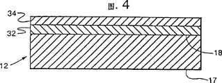
Fig. 4 is the sectional view of panel, and it is superimposed on existing conductive layer to demonstrate photoconductive layer.
Fig. 5 is another embodiment of the luminescent screen assembly of ray tube shown in Figure 1.
Fig. 6 is the panel schematic diagram that is installed in the process for making in the spray equipment.
What Fig. 1 showed is a colour display device, and for example CRT 10, and it is to have a bag Draw together rectangular faceplate screen dish 12 and be connected the glass envelope of the neck 14 that rectangle cone 15 connects 11. Cone 15 has an internal conductive coating (not shown), and this coating contacts also with anode button 16 Extend in the neck 14. Screen dish 12 comprises that one has the observation panel 17 of an inner surface 18 With a circumferential flange or sidewall 20, this screen dish is sealed to cone 15 by a glass glaze 21 On. Tricolour phosphor screen 22 is installed on the inner surface 18 of observing panel 17, Fig. 2 institute The fluorescent screen 22 that shows is a line style fluorescent screen preferably, and it comprises multiple fluorescent screen element, this It is red that a little elements contain respectively emission, transmitting green and the blue fluorescence vitta of emission, R, G and B, they line up yi word pattern or isosceles triangle in the mode of circulation, and along colliding with generation This arrangement is extended on the plane that electron beam is vertical. In this routine overview position, iridescent Bar vertically stretches. Known to prior art, the fluorescence vitta is preferably by an absorption optical Host material 23 separate mutually. On the other hand, this fluorescent screen can be that a round dot is glimmering Optical screen. With a thin conductive layer 24, preferred aluminium covers above the fluorescent screen 22, from And a kind of device is provided so as to fluorescent screen apply even voltage and the reflection by fluorescence unit Part is launched, and passes the light of panel 17. Fluorescent screen 22 and covering aluminium lamination 24 formations one are glimmering Optical screen assembly 25.
According to Fig. 1, with usual manner a porous color filtering electrode is installed movably again at predetermined space with respect to luminescent screen assembly 25, or shadow mask 26.Be installed in the neck 14 by centering by the electron gun shown in the dotted line 27 among Fig. 1, it arrives on the phosphor screen 22 along the hole of receiving the sword trajectory generation and guide three electron beams 28 to pass in the shadow mask 26, this rifle 27 can, for example comprise bipotential electron gun or any other suitable rifle.
Ray tube 10 is designed to and an external magnetic deflecting coil, for example deflecting coil 30 uses together, this coil is positioned at the joint area of cone to neck, when being activated, coil 30 places under the influence in magnetic field three electron beams 28, this magnetic field energy make this electron beam 28 on phosphor screen 22 with the horizontal and vertical scanning of the mode of rectangular raster.Initial deflection plane (in zero deflection) is by the roughly middle part that is positioned at coil 30 shown in Fig. 1 center line P-P.For for simplicity, in the deflecting region, the actual curve of deflection beam track does not show.
In order to form matrix 23, use a corona charging device that OPC layer 34 is charged into+suitable voltage in 200 to+700 volts of scopes by the EPS method.Shadow mask 26 is inserted screen dish 12, the OPC layer 34 that fills positive electricity is passed through shadow mask 26, be exposed to actinic radiation, for example in the light from xenon flash lamp, this lamp is configured within the conventional three-in-one exposure desk (not shown), all lamp is moved on to a different position after each exposure, with the electron beam incident angle that repeats to send from electron gun.Need carry out from three different bulb positions zone discharge that three exposures make OPC layer 34 subsequently herein light emitting phosphor will deposit with formation fluorescent material 22.After the step of exposure, remove shadow mask 26, the screen dish is moved on to the first developer (not shown) from screen dish 12.This developer has the dry powder particle of the extinction black matix fluorescence structure material of corresponding preparation, the developer negative electrode triboelectric charging of this host material.The host material of negative electrode charging can directly be deposited in one step, perhaps can directly be deposited in two steps." two steps " apposition method can improve the opacity of gained matrix 23.Photoemissive fluorescent material is deposited in the mode described in the above-mentioned United States Patent (USP) 4921767 then.
Also can form matrix with the conventional wet basis matter method of prior art known type.If form matrix with wet process, on this matrix, form photoreceptor so, and deposit fluorescent material by mode described in the above-mentioned United States Patent (USP) 4921767.
As substituting of above-mentioned two " matrix first " technologies, in the formation matrix 123 of taking a picture by available electron after the EPS process deposits fluorescence light powder.Luminescent screen assembly 125 shown in Figure 5 contains phosphor screen 122, matrix element 123 and the superimposed aluminium lamination of making according to " matrix is last " technology 124.
In " matrix is last " technology, red, blue and green emitting fluorescence part, the particle of R, B and the G fluorescence structure material by depositing anodal triboelectric charging in turn forms respectively to filling on the positive electricity OPC layer 34 of photoreceptor.Charging process is with above-described identical.After three kinds of fluorescent material depositions, again with OPC layer 34 uniform charging to a positive potential, the screen dish 12 that will contain phosphor material powder places (not shown) on the matrix developer, and this just provides a friction negative electrical charge to the matrix fluorescence structure material.The open region OPC layer 34 that fills positive electricity of keeping apart the phosphor screen element deposits to this open region and is formed matrix 123 by chemical development by the host material that will fill negative electricity.The method is known as " directly " development.Then fluorescence structure material by above-mentioned United States Patent (USP) 4921767 described fixing and film forming.On phosphor screen 122, provide aluminium lamination 124 its purposes the same with the above-mentioned layer 24 that provides.
Have the luminescent screen assembly 25 of calorize or 125 panel 12 and toast the component volatilization that made luminescent screen assembly in about 20-30 minute at about 425 ℃ then, be to be understood that above-described phosphor screen manufacturing process can be modified, the triboelectric charge polarity of the charge polarity that provides on OPC layer 34 promptly being provided and being inducted on fluorescence structure material just can obtain a kind of luminescent screen assembly identical with said structure.
With reference to figure 4 and 6, to the inner surface 18 of panel 17, form OC layer 32 by spraying a kind of volatility organic conductive solution.This solution is different from the conducting solution of previously known, it is made up of following material basically, a kind of polyelectrolyte, it is selected from the vinyl imidazole salt (VIM) of poly-(dimethyl-diallyl-ammonium chloride) and methylsulfuric acid ester and the copolymer of vinyl pyrrolidone (VP), PVP (PVP); With a kind of diluent, it is selected from ethanol, first alcohol and water.
Poly-(dimethyl-diallyl-ammonium chloride) can be from CalgonCorp.Pittsburgh, and PA buys as Cat-Floc-CL or CAT Floc-T-2, and the copolymer of VTM and VP can be from BASF Corp., Parsippany, and NJ. buys as LuviquatMS-905.The Cat-Floc material of buying contains polyelectrolyte and is dissolved in inorganic salts in the water, for example NaCl and K
2SO
4, when they are used to prepare the OC layer, the not exclusively oven dry of screen dish baking back.The Cat-Floc material of being bought must be removed the chloride ion in the inorganic salts before it is used to prepare the organic conductive body, or its concentration is reduced, because chloride ion was harmful to the ray tube life-span.
In order to remove or to reduce chloride ion on the organic polymer chain that is combined in the Cat-Floc material, the Cat-Floc solution with 10% is dissolved in three times the distilled water and mixed two hours with 10% solid anion exchange bead.Then the filter-press of this mixture by 5 μ filtered, in solution, be settled out with acetone through the Cat-Floc of ion-exchange.Then acetone and the water of sediment with 80: 20 is washed, and be dissolved in and make the Cat-Floc aqueous solution that contains 50 weight % in the water.The pH value of Cat-Floc that has reduced chlorine is in the scope of 12-13.With HNO O.1%
3Or 0.1% H
3PO
4By titration PH is adjusted to 4.
Following embodiment is used for being described in more detail OC layer 32, and is the restriction to it anything but.
OC embodiment 1
Filter a kind of organic conductive solution of formation by the following component of thorough mixing 1 hour and with this solution by 1 (um) micron filter.
140 gram (0.67 weight % solid) Cat-Floc-Cl 50% solution in water;
350 gram (0.33 weight % solid) PVP 10% solution in methyl alcohol; With
10,010 gram methyl alcohol
In last example, all or part of replacement methyl alcohol of available ethanol, yet ethanol than methyl alcohol boiling point height, therefore it is longer drying time as the solution of diluent than containing methyl alcohol as the solution of diluent to contain ethanol.The quantity of water only is 0.67 weight % and is that form with Cat-Floc solution exists in last routine solution; Yet can add more water as diluent, but the drying time of this solution is longer as the drying time of the solution of diluent than only containing methyl alcohol.
OC embodiment 2
Mix and filter following component according to mode described in the OC embodiment 1 and form second kind of organic conductive solution.
75-100 restrains (3 weight % solid) MS-905, the copolymer of a kind of vinyl imidazole of methylsulfuric acid ester (VIM) and vinyl pyrrolidone (VP); With
925-900 restrains (surplus) methyl alcohol.
As shown in Figure 6, OC solution is on the inner surface 18 that sprays to panel 17 under the pressure and along the interior face portion spraying of the sidewall 20 of screen dish 12 with a spray equipment 40, this sprayer unit 40 has a nozzle 42 movably, and this nozzle can form the flat spray greater than 110 ° of dispersion angle θ.The pressure of spray solution is provided by jar 44, and it is with 2.8kg/cm
2Spray pressure (40psi) is operated and is connected to nozzle 42 by spraying pipeline 46.Distance between the inner surface 18 of nozzle 42 and screen dish 12 approximately is half of screen dish diagonal-size with 3: 4 aspect ratios.For example for 51cm (20V) screen dish, this distance is about 25cm (10-20 inch).Coiling this distance for the screen with 9: 16 aspect ratios can suitably be adjusted so that suitable effective range to be provided.It is about 1 micron OC layer 32 that the single channel nozzle 42 of leap observation panel 17 inner surfaces 18 is enough to provide thickness.When diluent was methyl alcohol, OC layer 32 approximately was 30 to 45 seconds in the air drying time of about 50 ℃ of temperature.The OC layer of explained hereafter is continuous thus, yet, can believe that unique requirement is exactly that the OC layer provides an adjacency, promptly basic continuous coating, it will play grounding electrode in the EPS process.The OC layer 32 of using the phase spraying coating process can be used to above-described or " matrix first " or " matrix is last " technology, or is used to not have on the matrix screen dish.
After OC layer 32 drying, can be applied to OPC layer 34 by conventional " spin coating ", wherein the OPC solution of some is dispersed in screen and coils on the OC layer 32 on 12 inner surfaces 18, the rotary screen dish is dispersed in OPC solution on the OPC layer that forms the about 5-6 μ of thickness on the whole OC layer.At least a portion must extend beyond OPC layer 34 along the OC layer 32 of sidewall 20 inner surfaces, thereby provides an electric contact to OC layer 32.Any several known OPC prescription all can be used to form OPC layer 34; Yet following prescription is rapidly dry, has good electricity and physical property, is preferred therefore.
This OPC solution has following component:
300 gram (10 weight %) polystyrene;
50 gram (1.66 weight %) 1,4-two (2, the 4-aminomethyl phenyl)-1,4-diphenyl fourth
Triolefin (2,4 DMPBT)
2.5 gram (0.083 weight %) 2,4,7-trinitro--9-Fluorenone (TNF);
7.5 gram (0.25 weight %) 2-EAQ (2-EAQ);
0.15 gram (0.005 weight %) polysiloxanes U-7602; With
2648 gram (surplus) toluene.
Surfactant U-7602 can be from Union Carbide, and Danbury CT buys.For preparation OPC solution, be added to polystyrene resin in the toluene and stir and dissolve fully until this resin.Then electron donor material, 2,4-DMPBT, and electron acceptor material (TNF) and (2-EAQ) be added in the solution and stir.When agitating solution, add surfactant, polysiloxanes U-7602 stirs and carries out till whole components are all dissolved continuously always.The solution of gained filters by filter a series of series connection and that have from 10 to 0.5 μ opening size scopes.
Claims (9)
1. observation panel (17) inner surface (18) at screen dish (12) is gone up the method for preparing color cathode ray tube (10) luminescent screen assembly (25,125), may further comprise the steps:
Apply the described inner surface of described observation panel and form volatilizable organic conductive layers (32); With
With the described organic conductive layers of a kind of organic photoconductive solution brushing, form volatilizable organic photoelectric conducting shell (34); It is characterized in that:
Apply the step that described inner surface forms volatilizable organic conductive layers and comprise some substeps:
A kind of organic conductive solution is provided, and it contains the vinyl imidazole salt that is selected from poly-(dimethyl-diallyl-ammonium chloride), methylsulfuric acid ester and the polyelectrolyte of vinylpyrrolidone copolymers and PVP; With at least a diluent that is selected from ethanol, first alcohol and water; With
Spray described organic conductive solution to the described inner surface of described panel and form described volatilizable organic conductive layers, this organic conductive layers is continuous and provides an electrode for described covering organic photoelectric conducting shell thereon.
2. the method for claim 1, wherein said organic conductive solution contains:
0.67 weight % gathers (dimethyl-diallyl-ammonium chloride); 0.33 weight % polyvinylpyrrolidone; With surplus be at least a diluent, it is selected from ethanol, the first alcohol and water.
3. method as claimed in claim 2, wherein said diluent comprises the first alcohol and water.
4. the method for claim 1, wherein said organic solution comprises:
The vinyl imidazole salt and the vinylpyrrolidone copolymer of the methylsulfuric acid ester of 3 weight %, and the methyl alcohol of surplus.
5. the method for claim 1, wherein said spraying step comprises:
The described inner surface (18) of described panel (17) is arranged on from the suitable distance of spray equipment (40);
Described organic conductive solution is distributed on the described inner surface in the mode of putting down spray substantially from the nozzle (42) of described device; Then
With the dry described solution of the air of elevated temperature.
6. method as claimed in claim 5, wherein said organic conductive solution is with 2.8kg/cm
2Pressure spray.
7. method as claimed in claim 5, wherein said suitable distance approximately are half of described screen dish (12) diagonal-size.
8. method as claimed in claim 5, wherein said flat spray has the dispersion angle greater than 110 °.
9. method as claimed in claim 5, wherein said drying steps are 50 ℃, 30 to 45 seconds drying times.
Applications Claiming Priority (3)
| Application Number | Priority Date | Filing Date | Title |
|---|---|---|---|
| US168488 | 1993-12-22 | ||
| US168,488 | 1993-12-22 | ||
| US08/168,488 US5407765A (en) | 1993-12-22 | 1993-12-22 | Method of spray-depositing an organic conductor to make a screen assembly for a CRT |
Publications (2)
| Publication Number | Publication Date |
|---|---|
| CN1110828A CN1110828A (en) | 1995-10-25 |
| CN1073271C true CN1073271C (en) | 2001-10-17 |
Family
ID=22611699
Family Applications (1)
| Application Number | Title | Priority Date | Filing Date |
|---|---|---|---|
| CN94120765A Expired - Fee Related CN1073271C (en) | 1993-12-22 | 1994-12-21 | Screening method including spray-depositing an organic conductor |
Country Status (6)
| Country | Link |
|---|---|
| US (1) | US5407765A (en) |
| JP (1) | JP3760418B2 (en) |
| KR (1) | KR0141565B1 (en) |
| CN (1) | CN1073271C (en) |
| CA (1) | CA2138189C (en) |
| PL (1) | PL177668B1 (en) |
Families Citing this family (2)
| Publication number | Priority date | Publication date | Assignee | Title |
|---|---|---|---|---|
| US6326110B1 (en) | 1999-08-23 | 2001-12-04 | Thomson Licensing S.A. | Humidity and temperature insensitive organic conductor for electrophotographic screening process |
| JP2008156551A (en) * | 2006-12-26 | 2008-07-10 | Nippon Electric Glass Co Ltd | Glass paste |
Citations (2)
| Publication number | Priority date | Publication date | Assignee | Title |
|---|---|---|---|---|
| US4921767A (en) * | 1988-12-21 | 1990-05-01 | Rca Licensing Corp. | Method of electrophotographically manufacturing a luminescent screen assembly for a cathode-ray-tube |
| CN1057734A (en) * | 1990-06-26 | 1992-01-08 | 汤姆森消费电子有限公司 | The method of electrophotographicamanufacturing manufacturing luminescent screen for color CRT |
Family Cites Families (5)
| Publication number | Priority date | Publication date | Assignee | Title |
|---|---|---|---|---|
| US3475169A (en) * | 1965-08-20 | 1969-10-28 | Zenith Radio Corp | Process of electrostatically screening color cathode-ray tubes |
| US3489556A (en) * | 1966-03-16 | 1970-01-13 | Zenith Radio Corp | Process fo electrostatically screening color cathode-ray tubes |
| NL7803025A (en) * | 1978-03-21 | 1979-09-25 | Philips Nv | PROCEDURE FOR MANUFACTURING A COLOR RATE-TV DISPLAY TUBE AND TUBE THEREFORE MANUFACTURED. |
| US4282118A (en) * | 1978-11-15 | 1981-08-04 | Calgon Corporation | Electroconductive polymer composition |
| US4990416A (en) * | 1989-06-19 | 1991-02-05 | Coloray Display Corporation | Deposition of cathodoluminescent materials by reversal toning |
-
1993
- 1993-12-22 US US08/168,488 patent/US5407765A/en not_active Expired - Lifetime
-
1994
- 1994-12-15 CA CA002138189A patent/CA2138189C/en not_active Expired - Fee Related
- 1994-12-21 CN CN94120765A patent/CN1073271C/en not_active Expired - Fee Related
- 1994-12-21 JP JP31877394A patent/JP3760418B2/en not_active Expired - Fee Related
- 1994-12-22 KR KR1019940035927A patent/KR0141565B1/en not_active IP Right Cessation
- 1994-12-22 PL PL94306479A patent/PL177668B1/en not_active IP Right Cessation
Patent Citations (2)
| Publication number | Priority date | Publication date | Assignee | Title |
|---|---|---|---|---|
| US4921767A (en) * | 1988-12-21 | 1990-05-01 | Rca Licensing Corp. | Method of electrophotographically manufacturing a luminescent screen assembly for a cathode-ray-tube |
| CN1057734A (en) * | 1990-06-26 | 1992-01-08 | 汤姆森消费电子有限公司 | The method of electrophotographicamanufacturing manufacturing luminescent screen for color CRT |
Also Published As
| Publication number | Publication date |
|---|---|
| PL177668B1 (en) | 1999-12-31 |
| KR0141565B1 (en) | 1998-06-01 |
| CA2138189A1 (en) | 1995-06-23 |
| JP3760418B2 (en) | 2006-03-29 |
| US5407765A (en) | 1995-04-18 |
| JPH07235265A (en) | 1995-09-05 |
| PL306479A1 (en) | 1995-06-26 |
| CA2138189C (en) | 1999-06-01 |
| KR950020875A (en) | 1995-07-26 |
| CN1110828A (en) | 1995-10-25 |
Similar Documents
| Publication | Publication Date | Title |
|---|---|---|
| RU2067334C1 (en) | Manufacture of luminescent screen assembly on cathode-ray tube substance and of luminescent screen assembly on inner surface of faceplate panel for color cathode-ray tube electrophotography method | |
| EP0378911B1 (en) | Method of electrophotographically manufacturing a luminescent screen assembly for a cathode-ray tube | |
| RU2051440C1 (en) | Electrographic method of manufacture of luminescent screen unit on backing of color cathode-ray tube and luminescent screen unit on inner surface of frontal panel of color cathode-ray tube | |
| JPH02283789A (en) | Method for surface treatment of dried powdery phosphor particle used for manufacture of cathode ray tube screen, and cathode ray tube | |
| CN1073272C (en) | Combined baking-out and sealing of electrophotographically screened CRT | |
| US5012155A (en) | Surface treatment of phosphor particles and method for a CRT screen | |
| US5156770A (en) | Conductive contact patch for a CRT faceplate panel | |
| US5413885A (en) | Organic photoconductor for an electrophotographic screening process for a CRT | |
| KR0158023B1 (en) | Organic conductor for an electrophotographic screening process for crt | |
| US5135826A (en) | Method of electrophotographically manufacturing a luminescent screen assembly for a crt using an improved plasticizer for a photoconductive layer | |
| CN1073271C (en) | Screening method including spray-depositing an organic conductor | |
| EP0375229B1 (en) | Surface treatment of phosphor particles and method for a crt screen | |
| JP3716167B2 (en) | Electrophotographic screening method with organic conductors independent of humidity and temperature | |
| US6040097A (en) | Solution for making photoconductive layer and an electrophotographic manufacturing method of the layer in CRT | |
| KR100202870B1 (en) | Method of forming lacquer film in manufacturing electrophotographic screen of cathode ray tube |
Legal Events
| Date | Code | Title | Description |
|---|---|---|---|
| C10 | Entry into substantive examination | ||
| SE01 | Entry into force of request for substantive examination | ||
| C06 | Publication | ||
| PB01 | Publication | ||
| C14 | Grant of patent or utility model | ||
| GR01 | Patent grant | ||
| C17 | Cessation of patent right | ||
| CF01 | Termination of patent right due to non-payment of annual fee |
Granted publication date: 20011017 Termination date: 20100121 |