CN107112208B - Photocurable composition and its application - Google Patents
Photocurable composition and its application Download PDFInfo
- Publication number
- CN107112208B CN107112208B CN201580069521.5A CN201580069521A CN107112208B CN 107112208 B CN107112208 B CN 107112208B CN 201580069521 A CN201580069521 A CN 201580069521A CN 107112208 B CN107112208 B CN 107112208B
- Authority
- CN
- China
- Prior art keywords
- film
- imprinting
- meth
- photocurable composition
- polymerizable compound
- Prior art date
- Legal status (The legal status is an assumption and is not a legal conclusion. Google has not performed a legal analysis and makes no representation as to the accuracy of the status listed.)
- Active
Links
Images


Classifications
-
- G—PHYSICS
- G03—PHOTOGRAPHY; CINEMATOGRAPHY; ANALOGOUS TECHNIQUES USING WAVES OTHER THAN OPTICAL WAVES; ELECTROGRAPHY; HOLOGRAPHY
- G03F—PHOTOMECHANICAL PRODUCTION OF TEXTURED OR PATTERNED SURFACES, e.g. FOR PRINTING, FOR PROCESSING OF SEMICONDUCTOR DEVICES; MATERIALS THEREFOR; ORIGINALS THEREFOR; APPARATUS SPECIALLY ADAPTED THEREFOR
- G03F7/00—Photomechanical, e.g. photolithographic, production of textured or patterned surfaces, e.g. printing surfaces; Materials therefor, e.g. comprising photoresists; Apparatus specially adapted therefor
- G03F7/0002—Lithographic processes using patterning methods other than those involving the exposure to radiation, e.g. by stamping
-
- G—PHYSICS
- G03—PHOTOGRAPHY; CINEMATOGRAPHY; ANALOGOUS TECHNIQUES USING WAVES OTHER THAN OPTICAL WAVES; ELECTROGRAPHY; HOLOGRAPHY
- G03F—PHOTOMECHANICAL PRODUCTION OF TEXTURED OR PATTERNED SURFACES, e.g. FOR PRINTING, FOR PROCESSING OF SEMICONDUCTOR DEVICES; MATERIALS THEREFOR; ORIGINALS THEREFOR; APPARATUS SPECIALLY ADAPTED THEREFOR
- G03F7/00—Photomechanical, e.g. photolithographic, production of textured or patterned surfaces, e.g. printing surfaces; Materials therefor, e.g. comprising photoresists; Apparatus specially adapted therefor
- G03F7/004—Photosensitive materials
- G03F7/027—Non-macromolecular photopolymerisable compounds having carbon-to-carbon double bonds, e.g. ethylenic compounds
-
- C—CHEMISTRY; METALLURGY
- C08—ORGANIC MACROMOLECULAR COMPOUNDS; THEIR PREPARATION OR CHEMICAL WORKING-UP; COMPOSITIONS BASED THEREON
- C08F—MACROMOLECULAR COMPOUNDS OBTAINED BY REACTIONS ONLY INVOLVING CARBON-TO-CARBON UNSATURATED BONDS
- C08F2/00—Processes of polymerisation
- C08F2/46—Polymerisation initiated by wave energy or particle radiation
- C08F2/48—Polymerisation initiated by wave energy or particle radiation by ultraviolet or visible light
- C08F2/50—Polymerisation initiated by wave energy or particle radiation by ultraviolet or visible light with sensitising agents
-
- G—PHYSICS
- G02—OPTICS
- G02B—OPTICAL ELEMENTS, SYSTEMS OR APPARATUS
- G02B5/00—Optical elements other than lenses
- G02B5/18—Diffraction gratings
- G02B5/1847—Manufacturing methods
- G02B5/1857—Manufacturing methods using exposure or etching means, e.g. holography, photolithography, exposure to electron or ion beams
-
- G—PHYSICS
- G03—PHOTOGRAPHY; CINEMATOGRAPHY; ANALOGOUS TECHNIQUES USING WAVES OTHER THAN OPTICAL WAVES; ELECTROGRAPHY; HOLOGRAPHY
- G03F—PHOTOMECHANICAL PRODUCTION OF TEXTURED OR PATTERNED SURFACES, e.g. FOR PRINTING, FOR PROCESSING OF SEMICONDUCTOR DEVICES; MATERIALS THEREFOR; ORIGINALS THEREFOR; APPARATUS SPECIALLY ADAPTED THEREFOR
- G03F1/00—Originals for photomechanical production of textured or patterned surfaces, e.g., masks, photo-masks, reticles; Mask blanks or pellicles therefor; Containers specially adapted therefor; Preparation thereof
- G03F1/68—Preparation processes not covered by groups G03F1/20 - G03F1/50
- G03F1/80—Etching
-
- G—PHYSICS
- G03—PHOTOGRAPHY; CINEMATOGRAPHY; ANALOGOUS TECHNIQUES USING WAVES OTHER THAN OPTICAL WAVES; ELECTROGRAPHY; HOLOGRAPHY
- G03F—PHOTOMECHANICAL PRODUCTION OF TEXTURED OR PATTERNED SURFACES, e.g. FOR PRINTING, FOR PROCESSING OF SEMICONDUCTOR DEVICES; MATERIALS THEREFOR; ORIGINALS THEREFOR; APPARATUS SPECIALLY ADAPTED THEREFOR
- G03F7/00—Photomechanical, e.g. photolithographic, production of textured or patterned surfaces, e.g. printing surfaces; Materials therefor, e.g. comprising photoresists; Apparatus specially adapted therefor
- G03F7/004—Photosensitive materials
- G03F7/027—Non-macromolecular photopolymerisable compounds having carbon-to-carbon double bonds, e.g. ethylenic compounds
- G03F7/028—Non-macromolecular photopolymerisable compounds having carbon-to-carbon double bonds, e.g. ethylenic compounds with photosensitivity-increasing substances, e.g. photoinitiators
-
- G—PHYSICS
- G03—PHOTOGRAPHY; CINEMATOGRAPHY; ANALOGOUS TECHNIQUES USING WAVES OTHER THAN OPTICAL WAVES; ELECTROGRAPHY; HOLOGRAPHY
- G03F—PHOTOMECHANICAL PRODUCTION OF TEXTURED OR PATTERNED SURFACES, e.g. FOR PRINTING, FOR PROCESSING OF SEMICONDUCTOR DEVICES; MATERIALS THEREFOR; ORIGINALS THEREFOR; APPARATUS SPECIALLY ADAPTED THEREFOR
- G03F7/00—Photomechanical, e.g. photolithographic, production of textured or patterned surfaces, e.g. printing surfaces; Materials therefor, e.g. comprising photoresists; Apparatus specially adapted therefor
- G03F7/70—Microphotolithographic exposure; Apparatus therefor
- G03F7/70691—Handling of masks or workpieces
- G03F7/70775—Position control, e.g. interferometers or encoders for determining the stage position
-
- H10P76/4085—
-
- H10P76/20—
Landscapes
- Physics & Mathematics (AREA)
- General Physics & Mathematics (AREA)
- Chemical & Material Sciences (AREA)
- Engineering & Computer Science (AREA)
- Spectroscopy & Molecular Physics (AREA)
- Manufacturing & Machinery (AREA)
- Chemical Kinetics & Catalysis (AREA)
- Polymers & Plastics (AREA)
- Organic Chemistry (AREA)
- Medicinal Chemistry (AREA)
- Health & Medical Sciences (AREA)
- Optics & Photonics (AREA)
- Exposure Of Semiconductors, Excluding Electron Or Ion Beam Exposure (AREA)
- Condensed Matter Physics & Semiconductors (AREA)
- Computer Hardware Design (AREA)
- Microelectronics & Electronic Packaging (AREA)
- Power Engineering (AREA)
- Inorganic Chemistry (AREA)
- Shaping Of Tube Ends By Bending Or Straightening (AREA)
- Polymerisation Methods In General (AREA)
- Addition Polymer Or Copolymer, Post-Treatments, Or Chemical Modifications (AREA)
Abstract
一种压印用光固化性组合物,至少具有聚合性化合物(A)和光聚合引发剂(B),其中聚合性化合物(A)包含20重量%以上的多官能(甲基)丙烯酸系单体,且光固化性组合物的光固化物的玻璃化转变温度为90℃以上。
A photocurable composition for imprint, comprising at least a polymerizable compound (A) and a photopolymerization initiator (B), wherein the polymerizable compound (A) contains 20% by weight or more of a polyfunctional (meth)acrylic monomer , and the glass transition temperature of the photocured product of the photocurable composition is 90°C or higher.
Description
Technical Field
The present invention relates to a photocurable composition for imprinting, a method for producing a film using the same, a method for producing an optical module using the same, a method for producing a circuit board using the same, and a method for producing an electronic module using the same.
Background
The demand for miniaturization of semiconductor devices, MEMS, and the like is increasing. Therefore, in addition to the conventional photolithography technique, attention is being paid to a microfabrication technique using, as a mold, a resist (photocurable composition for nanoimprint) pattern formed on a substrate (wafer) and having a predetermined shape. This technique is also called a photo-imprint technique (photo nanoimprint), and can form a fine structure of several nanometers on a substrate (PTL 1). According to the photo imprint technique, first, a resist is applied to a pattern formation region on a substrate (arrangement step). Next, a resist is molded using a mold on which a pattern is formed (mold contact step). Then, the resist is cured by emitting light (irradiation step with light), and then the cured resist is separated (mold release step). By performing these steps, a pattern of a cured resist (photocurable film) having a predetermined shape is formed on the substrate. Further, by repeating all the above steps at other positions of the substrate, fine structures can be formed on all the substrates.
A patterned photocurable film formed on a substrate by a photoimprint technique is sometimes used as a mask in substrate processing using a dry etching technique. In this case, in order to process the substrate with good yield, the photocurable film is required to have high dry etching resistance. Further, in manufacturing semiconductor devices, it is required to form a circuit board with an accuracy of about ± 10-12% of a desired line width.
List of cited documents
Patent document
PTL 1: japanese patent laid-open No. 2007-186570
Disclosure of Invention
Problems to be solved by the invention
When a pattern of a cured resist is transferred into a circuit pattern by a dry etching technique, the cured resist undergoes thermal expansion due to reaction heat generated by etching. Therefore, when the thermal expansion coefficient of the cured resist is large, the line width of the pattern expands and deforms, which causes a problem that a circuit pattern with required accuracy cannot be obtained.
In addition, when the photo-imprint method is industrially employed, in order to obtain high productivity, it is required that after the photo-curable composition for imprinting is brought into contact with the mold, the photo-curable composition for imprinting quickly fills the concave portions of the fine pattern on the mold.
In order to solve the above problems, there is a need for a photocurable composition for imprinting having a small thermal expansion upon curing and having excellent filling properties.
The present invention provides a photocurable composition for imprinting having small thermal expansion in dry etching and excellent filling performance in a photoimprinting method. The present invention also provides a film manufacturing method using the photocurable composition for imprinting, a method of manufacturing an optical assembly using the same, a method of manufacturing a circuit board using the same, and a method of manufacturing an electronic assembly using the same.
Means for solving the problems
The present invention is a photocurable composition for imprinting having at least a polymerizable compound (a) and a photopolymerization initiator (B), wherein the polymerizable compound (a) contains 20 wt% or more of a polyfunctional (meth) acrylic monomer, and a glass transition temperature of a photocured product of the photocurable composition is 90 ℃ or higher.
Further features of the present invention will become apparent from the following description of exemplary embodiments with reference to the attached drawings.
Drawings
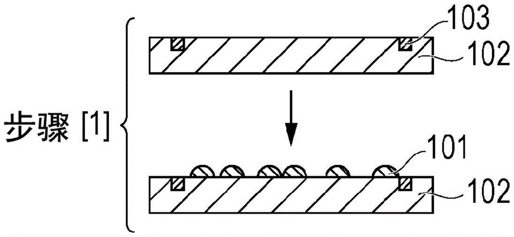
Fig. 1A is a schematic cross-sectional view showing an example of the film manufacturing method of the embodiment.
Fig. 1B includes fig. 1B (B-1) and 1B (B-2), and is a schematic sectional view showing an example of the method for producing a film of the present embodiment.
Fig. 1C is a schematic cross-sectional view showing an example of the method for producing a film of the present embodiment.
FIG. 1D includes FIG. 1D (D-1) and FIG. 1D (D-2), and is a schematic sectional view showing an example of the method for producing a film of the present embodiment.
Fig. 1E is a schematic cross-sectional view showing an example of the method for producing a film of the present embodiment.
Fig. 1F is a schematic cross-sectional view showing an example of the film production method of the present embodiment.
Fig. 1G is a schematic cross-sectional view showing an example of the method for producing a film of the present embodiment.
Detailed Description
Hereinafter, embodiments of the present invention will be described in detail with reference to appropriate drawings. However, the present invention is not limited to the following embodiments. In the present invention, those obtained by appropriately modifying or improving the following embodiments without departing from the gist of the present invention, for example, based on the general knowledge of those skilled in the art, are also encompassed in the scope of the present invention.
Photocurable composition for imprinting
In the present embodiment, the photocurable composition for imprinting is a curable composition including at least the following component (a) and component (B):
and (2) component A: a polymerizable compound; and
and (B) component: a photopolymerization initiator.
In particular, the photocurable composition for imprinting is suitable for forming a nano-scale (1nm to several hundred nm) pattern of a photocurable film on a substrate such as a semiconductor substrate, which is called nanoimprinting. Further, the photocurable composition for imprinting is also suitable for dry etching of a photocurable film formed by nanoimprinting to process a substrate.
In the present embodiment, the cured film refers to a film obtained by polymerizing a photocurable composition on a substrate and then curing. In addition, the photo-curable film may have a pattern shape.
Hereinafter, each component will be described in detail.
A component (A): polymerizable compound
The component (A) is a polymerizable compound. Here, in the present embodiment, the polymerizable compound refers to a compound that reacts with a polymerization factor (radical or the like) generated from a photopolymerization initiator (component (B)) to form a film containing a polymer compound by a chain reaction (polymerization reaction).
As such a polymerizable compound, for example, a radical polymerizable compound is mentioned. The polymerizable compound as the component (a) may include one polymerizable compound or two or more polymerizable compounds.
The radical polymerizable compound is suitably a compound having one or more acryloyl groups or methacryloyl groups, that is, a (meth) acrylic compound.
Therefore, the component (a) (polymerizable compound) of the nanoimprint photocurable composition suitably includes a (meth) acrylic compound. The main component of the component (a) is more suitably a (meth) acrylic compound. Most suitably, component (a) may contain only (meth) acrylic compounds. Here, the component (a) whose main component is a (meth) acrylic compound means that the component (a) contains 90% by weight or more of a (meth) acrylic compound.
When the radical polymerizable compound contains two or more compounds having one or more acryloyl groups or methacryloyl groups, the radical polymerizable compound suitably includes a monofunctional (meth) acrylic monomer and a polyfunctional (meth) acrylic monomer. This is because a photocurable film having high mechanical strength is obtained by the combination of a monofunctional acrylic monomer and a polyfunctional acrylic monomer. In the present embodiment, the polyfunctional (meth) acrylic monomer is suitably contained in a proportion of 25% by weight or more. Therefore, it is considered that the crosslinking density of the photo-cured film increases and the thermal expansion becomes small in the dry etching.
Examples of the monofunctional (meth) acrylic compound having one acryloyl group or methacryloyl group include, for example, phenoxyethyl (meth) acrylate, phenoxy-2-methylethyl (meth) acrylate, phenoxyethoxyethyl (meth) acrylate, 3-phenoxy-2-hydroxypropyl (meth) acrylate, 2-phenylphenoxyethyl (meth) acrylate, 4-phenylphenoxyethyl (meth) acrylate, 3- (2-phenylphenyl) -2-hydroxypropyl (meth) acrylate, EO-modified p-isopropylphenyl (meth) acrylate, 2-bromophenoxyethyl (meth) acrylate, 2, 4-dibromophenoxyethyl (meth) acrylate, 2,4, 6-tribromophenoxyethyl (meth) acrylate, and mixtures thereof, EO-modified phenoxy (meth) acrylate, PO-modified phenoxy (meth) acrylate, polyoxyethylene nonylphenyl ether (meth) acrylate, isobornyl (meth) acrylate, 1-adamantyl (meth) acrylate, 2-methyl-2-adamantyl (meth) acrylate, 2-ethyl-2-adamantyl (meth) acrylate, bornyl (meth) acrylate, tricyclodecyl (meth) acrylate, dicyclopentanyl (meth) acrylate, dicyclopentenyl (meth) acrylate, cyclohexyl (meth) acrylate, 4-butylcyclohexyl (meth) acrylate, acryloylmorpholine, 2-hydroxyethyl (meth) acrylate, 2-hydroxypropyl (meth) acrylate, 2-hydroxybutyl (meth) acrylate, polyoxyethylene (meth) acrylate, 2-hydroxypropyl (meth) acrylate, polyoxyethylene (meth), Methyl (meth) acrylate, ethyl (meth) acrylate, propyl (meth) acrylate, isopropyl (meth) acrylate, butyl (meth) acrylate, pentyl (meth) acrylate, isobutyl (meth) acrylate, tert-butyl (meth) acrylate, pentyl (meth) acrylate, isopentyl (meth) acrylate, hexyl (meth) acrylate, heptyl (meth) acrylate, octyl (meth) acrylate, isooctyl (meth) acrylate, 2-ethylhexyl (meth) acrylate, nonyl (meth) acrylate, decyl (meth) acrylate, isodecyl (meth) acrylate, undecyl (meth) acrylate, dodecyl (meth) acrylate, lauryl (meth) acrylate, stearyl (meth) acrylate, isostearyl (meth) acrylate, benzyl (meth) acrylate, and the like, 1-naphthylmethyl (meth) acrylate, 2-naphthylmethyl (meth) acrylate, tetrahydrofurfuryl (meth) acrylate, butoxyethyl (meth) acrylate, ethoxydiglycol (meth) acrylate, polyethylene glycol mono (meth) acrylate, polypropylene glycol mono (meth) acrylate, methoxyethylene glycol (meth) acrylate, ethoxyethyl (meth) acrylate, methoxypolyethylene glycol (meth) acrylate, methoxypolypropylene glycol (meth) acrylate, diacetone (meth) acrylamide, isobutoxymethyl (meth) acrylamide, N-dimethyl (meth) acrylamide, t-octyl (meth) acrylamide, dimethylaminoethyl (meth) acrylate, diethylaminoethyl (meth) acrylate, 7-amino-3 (meth) acrylate, 7-dimethyloctyl ester, N-diethyl (meth) acrylamide, N-dimethylaminopropyl (meth) acrylamide, and the like, but the monofunctional (meth) acrylic compound having one acryloyl group or methacryloyl group is not limited thereto.
Examples of commercially available products of monofunctional (meth) acrylic compounds include Aronix series M101, M102, M110, M111, M113, M117, M5700, TO-1317, M120, M150 and M156 (manufactured by Toagosei Co., Ltd.), MEDOL10, MIBDOL10, CHDOL10, MMDOL30, MEDOL30, MIBDOL30, CHDOL30, LA, IBXA, 2-MTA, HPA, Viscoat #150, #155, #158, #190, #192, #193, #220, #2000 and #2150(Osaka Organic Chemical Industry Co., manufactured by Ltd.), Light acrylate BO-2-A, DMP-A, HOP-A, HOA-MPE, AMP-63190, #193, #220, #2000 and #2150 (manufactured by Osaka Organic Chemical Industry Co., Ltd.), Ligno. TM.), Light acrylate BO-A, DMP-A, HOP-A, HOA-MPE, AMP, HOA-A, P-200-EA, 200-828, and Epstein series M-10, K-60, K-2, K-O-10, K-2, K-35, K-2, K-200, K-2-K-200, K-2, K-2-K-, FA-511A, 512A and 513A (Hitachi Chemical Co., Ltd.), PHE, CEA, PHE-2, PHE-4, BR-31M and BR-32(Daiichi Kogyo Seiyaku Co., Ltd.), Ltd., manufactured by Ltd.), VP (manufactured by BASF), ACMO, DMAA and DMAPAA (KOHJIN Film & Chemicals Co., manufactured by Ltd.), etc., but the commercially available products of monofunctional (meth) acrylic compounds are not limited thereto.
Examples of the polyfunctional (meth) acrylic compound having two or more acryloyl groups or methacryloyl groups include, for example, trimethylolpropane di (meth) acrylate, trimethylolpropane tri (meth) acrylate, EO-modified trimethylolpropane tri (meth) acrylate, PO-modified trimethylolpropane tri (meth) acrylate, EO, PO-modified trimethylolpropane tri (meth) acrylate, dimethylol tricyclodecane di (meth) acrylate, pentaerythritol tri (meth) acrylate, pentaerythritol tetra (meth) acrylate, ethylene glycol di (meth) acrylate, tetraethyleneethylene glycol di (meth) acrylate, phenyl ethylene glycol di (meth) acrylate, 2-phenyl-1, 3-propanediol diacrylate, polyethylene glycol di (meth) acrylate, poly (meth, Polypropylene glycol di (meth) acrylate, 1, 4-butanediol di (meth) acrylate, 1, 6-hexanediol di (meth) acrylate, neopentyl glycol di (meth) acrylate, 1, 9-nonanediol di (meth) acrylate, 1, 10-decanediol di (meth) acrylate, 1, 3-adamantanedimethanol di (meth) acrylate, o-xylene di (meth) acrylate, m-xylene di (meth) acrylate, p-xylene di (meth) acrylate, tris (2-hydroxyethyl) isocyanurate tri (meth) acrylate, tris (acryloyloxy) isocyanurate, bis (hydroxymethyl) tricyclodecane di (meth) acrylate, dipentaerythritol penta (meth) acrylate, dipentaerythritol hexa (meth) acrylate, and mixtures thereof, EO-modified 2, 2-bis (4- ((meth) acryloyloxy) phenyl) propane, PO-modified 2, 2-bis (4- ((meth) acryloyloxy) phenyl) propane, and EO, PO-modified 2, 2-bis (4- ((meth) acryloyloxy) phenyl) propane, and the like, but the polyfunctional (meth) acrylic compound having two or more acryloyl groups or methacryloyl groups is not limited thereto.
Examples of commercially available products of polyfunctional (meth) acrylic compounds are Yupimer UV SA1002 and SA2007 (manufactured by Mitsubishi Chemical Corporation), Viscoat #195, #230, #215, #260, #335HP, #295, #300, #360 and #700, GPT and 3PA (manufactured by Osaka Organic Chemical Industry Co., Ltd.), Light acrylate 4EG-A, 9EG-A, NP-A, DCP-A, BP-4EA, BP-4PA, TMP-A, PE-3A, PE-4A and DPE-6A (manufactured by Keisha Chemical Co., Ltd.), KAYARAD PET-30, TMPTA, R-604, DPHA and DPCA-20, -30, -60 and-120, HX-620, D-310 and D330 (manufactured by Nippon Kayaku Co., Lyaku. 208), Aroni M309, M, 210, 325, Hxam-120, HXM-620, D-310 and D330 (manufactured by Nippon Kayaku Chemical Co., Ltd.), Aroni M309, M.M.M.305, Toyakm.305, M.325, Toyak.M.M., ltd.), Ripoxy VR-77, VR-60 and VR-90 (manufactured by Showa Denko), etc., but examples of commercially available products are not limited thereto.
In the above-mentioned compound group, (meth) acrylate means acrylate or its corresponding methacrylate having an alcohol residue. (meth) acryloyl means acryloyl or its corresponding methacryloyl group having an alcohol residue. EO means ethylene oxide, and EO-modified Compound A means that the (meth) acrylic acid residue and the alcohol residue of Compound A are bonded to each other via a block structure of ethylene oxide groups; and PO means propylene oxide, and PO-modified compound B means that the (meth) acrylic acid residue and the alcohol residue of compound B are bonded to each other via a block structure of propylene oxide groups.
Ohnishi parameter of component (A)
The dry etching rate V of the composition, the total number N of atoms in the composition, the total number NC of carbon atoms in the composition, and the total number NO of oxygen atoms in the composition are known to have a relationship shown in the following expression (1) (j. electrochem. soc.,130, p143 (1983)).
VOCN/(NC-NO)(1)
In the expression (1), N/(N)C-NO) Commonly referred to as the "Ohnishi parameter". For example, PTL 1 discloses a technique of obtaining a photocurable composition having high dry etching resistance using a polymerizable compound component having a small Ohnishi parameter.
According to the above expression (1), it is taught that an organic compound having a smaller number of oxygen atoms or having a larger number of aromatic ring structures or aliphatic ring structures has a smaller Ohnishi parameter and has high dry etching resistance.
When the component (a) contains two or more polymerizable compounds, the Ohnishi parameter is calculated as a weighted average of molar fractions using the following expression (2).
OP=n1OP1+n2OP2+……+nnOPn(2)
In this embodiment, component (a) suitably has an ohnisi parameter of 3.2 or less. When component (a) is composed of a polymerizable compound in which the ohnisi parameter is less than 3.2, good dry etching resistance is obtained. On the other hand, when the component (a) is composed of a polymerizable compound in which the Ohnishi parameter is more than 3.2, dry etching resistance is poor, so that desired substrate processing accuracy cannot be obtained in some cases, which may lead to a decrease in productivity.
A component (B): photopolymerization initiator
The component (B) is a photopolymerization initiator.
In the present embodiment, the photopolymerization initiator is a compound that senses light of a predetermined wavelength to generate a polymerization factor (radical). Specifically, the photopolymerization initiator is a polymerization initiator (radical generator) that generates radicals by light (radiation rays such as infrared rays, visible rays, ultraviolet rays, far ultraviolet rays, X-rays, charged particle rays such as electron beams).
The component (B) may be composed of one photopolymerization initiator, or may be composed of two or more photopolymerization initiators.
Examples of the radical generator include, for example, 2,4, 5-triarylimidazole dimers which may have a substituent, such as 2- (o-chlorophenyl) -4, 5-diphenylimidazole dimer, 2- (o-chlorophenyl) -4, 5-bis (methoxyphenyl) imidazole dimer, 2- (o-fluorophenyl) -4, 5-diphenylimidazole dimer and 2- (o-or p-methoxyphenyl) -4, 5-diphenylimidazole dimer; benzophenone derivatives such as benzophenone, N '-tetramethyl-4, 4' -diaminobenzophenone (Michler's ketone), N' -tetraethyl-4, 4 '-diaminobenzophenone, 4-methoxy-4' -dimethylaminobenzophenones, 4-chlorobenzophenone, 4 '-dimethoxybenzophenone and 4, 4' -diaminobenzophenone; alpha-amino aromatic ketone derivatives such as 2-benzyl-2-methylamino-1- (4-morpholinophenyl) -butanone-1, 2-methyl-1- [4- (methylthio) phenyl ] -2-morpholinopropan-1-one; quinones such as 2-ethylanthraquinone, phenanthrenequinone, 2-tert-butylanthraquinone, octamethylanthraquinone, 1, 2-benzoanthraquinone, 2, 3-benzoanthraquinone, 2-phenylanthraquinone, 2, 3-diphenylanthraquinone, 1-chloroanthraquinone, 2-methylanthraquinone, 1, 4-naphthoquinone, 9, 10-phenanthrenequinone, 2-methyl-1, 4-naphthoquinone and 2, 3-dimethylanthraquinone; benzoin ether derivatives such as benzoin methyl ether, benzoin ethyl ether and benzoin phenyl ether; benzoin derivatives such as benzoin, methylbenzoin, ethylbenzoin and propylbenzoin; benzyl derivatives, such as benzyl dimethyl ketal; acridine derivatives, such as 9-phenylacridine and 1, 7-bis (9, 9' -acridinyl) heptane; n-phenylglycine derivatives such as N-phenylglycine; acetophenone derivatives such as acetophenone, 3-methylacetophenone, acetophenone benzyl ketal, 1-hydroxycyclohexyl benzophenone and 2, 2-dimethoxy-2-phenylacetophenone; thioxanthone derivatives such as thioxanthone, diethylthioxanthone, 2-isopropylthioxanthone and 2-chlorothioxanthone; acylphosphine oxide derivatives, such as 2,4, 6-trimethylbenzoyldiphenylphosphine oxide, bis (2,4, 6-trimethylbenzoyl) phenylphosphine oxide, bis (2, 6-dimethoxybenzoyl) -2,4, 4-trimethylpentylphosphine oxide; oxime ester derivatives, such as 1, 2-octanedione, 1- [4- (phenylthio) -,2- (O-benzoyloxime) ] and ethanone (ethanone), 1- [ 9-ethyl-6- (2-methylbenzoyl) -9H-carbazol-3-yl ] -,1- (O-acetyloxime); xanthone; a fluorenone; benzaldehyde; fluorene; anthraquinone; triphenylamine; carbazole; 1- (4-isopropylphenyl) -2-hydroxy-2-methylpropan-1-one, 2-hydroxy-2-methyl-1-phenylpropan-1-one, etc., but the radical generator is not limited thereto.
Examples of commercially available products of the radical generator include Irgacure 184, 369, 651, 500, 819, 907, 784 and 2959, CGI-1700, -1750, -1850 and CG24-61, Darocur 1116 and 1173, Lucirin TPO, LR8893 and LR8970 (manufactured by BASF), and Uvecryl P36 (manufactured by UCB), etc., but commercially available products are not limited thereto.
Of the above, the component (B) of the nanoimprint photocurable composition is suitably an acylphosphine oxide polymerization initiator.
In the above examples, the acylphosphine oxide polymerization initiator is an acylphosphine oxide compound such as 2,4, 6-trimethylbenzoyldiphenylphosphine oxide, bis (2,4, 6-trimethylbenzoyl) phenylphosphine oxide or bis (2, 6-dimethoxybenzoyl) -2,4, 4-trimethylpentylphosphine oxide.
The compounding ratio of the component (B) as a photopolymerization initiator in the nanoimprint photocurable composition is suitably 0.01% by weight or more and 10% by weight or less, more suitably 0.1% by weight or more and 7% by weight or less, based on the total amount of the component (a) as a polymerizable compound.
By setting the compounding ratio of the component (B) to 0.01 wt% or more based on the total amount of the polymerizable compound, the curing rate of the composition is increased, and the reaction efficiency can be improved. The obtained photocurable film is a photocurable film having a certain degree of mechanical strength by setting the compounding ratio of the component (B) to 10% by weight or less based on the total amount of the polymerizable compound.
Other additive Components (C)
The photocurable composition for nanoimprinting of this embodiment may further include an additive component (C) according to various purposes within a range not impairing the effects of the present invention, in addition to the above-described component (a) and component (B). Examples of such additive component (C) include a sensitizer, a hydrogen donor, an internal addition type release agent, a surfactant, an antioxidant, a solvent, a polymer component, a polymerization initiator other than component (B), and the like.
The sensitizer is a compound that is suitably added for the purpose of promoting the polymerization reaction and improving the reaction conversion rate. As the sensitizer, for example, a sensitizing dye and the like are mentioned.
The sensitizing dye is a compound which is excited by absorbing light of a specific wavelength and interacts with a photopolymerization initiator as the component (B). The interaction described here is energy transfer or electron transfer from the sensitized dye in an excited state to the photopolymerization initiator as the component (B).
Specific examples of the sensitizing dye include anthracene derivatives, anthraquinone derivatives, pyrene derivatives, perylene derivatives, carbazole derivatives, benzophenone derivatives, thioxanthone derivatives, xanthone derivatives, coumarin derivatives, phenothiazine derivatives, camphorquinone derivatives, acridine dyes, thiopyrylium salt dyes, merocyanine dyes, quinoline dyes, styrylquinoline dyes, coumarone dyes, thioxanthene dyes, xanthene dyes, oxonol dyes, cyanine dyes, rhodamine dyes, pyrylium salt dyes, and the like, but the sensitizing dye is not limited thereto.
The sensitizer may be used alone or as a mixture of two or more.
The hydrogen donor is a compound that reacts with an initiating radical generated from a photopolymerization initiator as the component (B), or a radical at the end of polymerization growth, thereby generating a radical having higher reactivity. When the photopolymerization initiator as the component (B) is a photo radical generator, a hydrogen donor is suitably added.
Specific examples of such hydrogen donors include, but are not limited to, amine compounds such as N-butylamine, di-N-butylamine, tri-N-butylphosphine, allylthiourea, s-benzylisothiouronium p-toluenesulfonate, triethylamine, diethylaminoethyl methacrylate, triethylenetetramine, 4' -bis (dialkylamino) benzophenone, ethyl N, N-dimethylaminobenzoate, isoamyl N, N-dimethylaminobenzoate, pentyl-4-dimethylaminobenzoate, triethanolamine and N-phenylglycine; mercapto compounds such as 2-mercapto-N-phenylbenzimidazole, mercaptopropionate, and the like, but the hydrogen donor is not limited thereto.
The hydrogen donor may be used alone or as a mixture of two or more thereof.
The hydrogen donor may have a function as a sensitizer.
When the photocurable composition for nanoimprinting of this embodiment includes a sensitizer or a hydrogen donor as the additive component (C), the content of each of the sensitizer and the hydrogen donor is suitably 0.1% by weight or more and 20% by weight or less, more suitably 0.1% by weight or more and 5.0% by weight or less, and still more suitably 0.2% by weight or more and 2.0% by weight or less, based on the total amount of the polymerizable compound as the component (a). When the sensitizer is contained in a proportion of 0.1 wt% or more based on the total amount of the component (a), the polymerization promoting effect can be more effectively exhibited. By setting the content of the sensitizer or hydrogen donor to 5.0 wt% or less, the molecular weight of the polymer compound constituting the cured film to be produced becomes sufficiently high, and poor dissolution in the nanoimprint photocurable composition or deterioration in the storage stability of the nanoimprint photocurable composition can be suppressed.
An internal addition type release agent may be added to the photocurable composition for nanoimprinting for the purpose of reducing the interfacial bonding force between the mold and the resist, that is, the release force in the release step. In the present specification, the internal addition type means that a release agent is previously added to a curable composition before a step of disposing a nanoimprint photocurable composition.
As the internal addition type release agent, surfactants such as silicone-based surfactants, fluorine-based surfactants, hydrocarbon-based surfactants, and the like can be used. In the present embodiment, the internal addition type release agent does not have polymerizability.
The fluorine-based surfactant includes polyoxyalkylene group (e.g., polyoxyethylene, polyoxypropylene, etc.) adducts of alcohols having a perfluoroalkyl group, and polyoxyalkylene group (e.g., polyoxyethylene, polyoxypropylene, etc.) adducts of perfluoropolyethers. The fluorine-based surfactant may have a hydroxyl group, an alkoxy group, an alkyl group, an amino group, a thiol group, and the like in a part of the molecular structure (e.g., terminal group).
As the fluorine-based surfactant, commercially available products can be used. Examples of commercially available Products include, for example, Megafac F-444, TF-2066, TF-2067 and TF-2068 (manufactured by DIC), Fluorad FC-430 and FC-431 (manufactured by Sumitomo 3M Limited), Surflon S-382 (manufactured by AGC), EFTOP EF-122A, 122B, 122C, EF-121, EF-126, EF-127 and MF-100 (manufactured by Tokem Products Co., Ltd.), PF-636, PF-6320, PF-656 and PF-6520 (manufactured by OMNOVA Solutions), Unidyne DS-401, DS-403 and DS-451 (manufactured by Daikin Industries), and Ftergene 250, 222F and 208G (manufactured by Neos Co., Ltd.), and the like.
The internal additive mold release agent may be a hydrocarbon surfactant.
The hydrocarbon surfactant includes an alkyl alcohol polyoxyalkylene-based adduct obtained by adding an oxyalkylene group having 2 to 4 carbon atoms to an alkyl alcohol having 1 to 50 carbon atoms, and the like.
Examples of the alkyl alcohol polyoxyalkylene-based adduct include ethylene oxide adduct of methyl alcohol, ethylene oxide adduct of decyl alcohol, ethylene oxide adduct of lauryl alcohol, ethylene oxide adduct of cetyl alcohol, ethylene oxide adduct of stearyl alcohol, ethylene oxide/propylene oxide adduct of stearyl alcohol, and the like. The terminal group of the alkyl alcohol polyoxyalkylene base adduct is not limited to the hydroxyl group, and it can be prepared by simply adding a polyoxyalkylene base to an alkyl alcohol. The hydroxyl group may be converted into other substituents, for example, polar functional groups such as carboxyl, amino, pyridyl, thiol or silanol groups, and hydrophobic functional groups such as alkyl and alkoxy groups.
As the polyoxyalkylene-based adduct of an alkyl alcohol, commercially available products can be used. Examples of commercially available commercial products include, for example, polyoxyethylene methyl ether (ethylene oxide adduct of methanol) manufactured by Aoki Oil Industrial Co., Ltd. (BLAUNON MP-400, MP-550 and MP-1000); polyoxyethylene decyl ether (ethylene oxide adduct of decyl alcohol) produced by Aoki Oil Industrial Co., Ltd. (FINESURF D-1303, FINESURF D-1305, D-1307 and D-1310); polyoxyethylene lauryl ether (ethylene oxide adduct of lauryl alcohol) produced by Aoki Oil Industrial co., ltd. (BLAUNON EL-1505); polyoxyethylene cetyl ether (ethylene oxide adduct of cetyl alcohol) (BLAUNON CH-305 and CH-310) manufactured by Aoki Oil Industrial co., ltd.; polyoxyethylene stearyl ether (ethylene oxide adduct of stearyl alcohol) manufactured by Aoki Oil Industrial co., ltd. (BLAUNON SR-705, SR-707, SR-715, SR-720, SR-730, and SR-750); aoki Oil Industrial Co., Ltd., a polyoxyethylene polyoxypropylene stearyl ether of random polymerization type (BLAUNON SA-50/501000R and SA-30/702000R); polyoxyethylene methyl ether made by BASF; and polyoxyethylene alkyl ethers (Emulgen series) produced by Kao Corporation, and the like.
Of these hydrocarbon surfactants, the internal addition type release agent is preferably a polyoxyethylene adduct of an alkyl alcohol, more preferably a polyoxyalkylene adduct of a long-chain alkyl alcohol.
The internal addition type release agent may be used alone or as a mixture of two or more thereof.
When the photocurable composition for imprints of the embodiment contains an internal addition type release agent as the additive component (C), the content of the internal addition type release agent is 0.001% by weight or more and 10% by weight or less based on the total amount of the polymerizable compound as the component (a). The content is suitably 0.01% by weight or more and 7% by weight or less, more suitably 0.05% by weight or more and 5% by weight or less.
The ratio of the component (a) to the component (B) can be determined by analyzing the photocurable composition for nanoimprinting of the embodiment and/or the photocurable film prepared by curing the same by infrared spectroscopy, ultraviolet-visible spectroscopy, or thermal gas chromatography/mass spectrometry, or the like, and thus, the ratio of the component (a) to the component (B) in the photocurable composition for nanoimprinting can be determined. Further, when the additive component (C) is contained, the proportions of the component (a), the component (B), and the component (C) in the photocurable composition for imprinting can be similarly determined.
Glass transition temperature of photocurable composition for imprinting
The glass transition temperature of the photocurable material of the photocurable composition for imprint of the present embodiment is suitably 90 ℃ or higher, more suitably 120 ℃ or higher. It is considered that thermal expansion and thermal deformation hardly occur in dry etching by setting the glass transition temperature to 90 ℃ or higher.
As a method for measuring the glass transition temperature of a photo-cured product, a Differential Scanning Calorimeter (DSC) or a dynamic viscoelasticity apparatus can be used to measure the glass transition temperature.
For example, when the glass transition temperature is measured by DSC, an extrapolated glass transition start temperature (Tig) is determined from the intersection of a straight line obtained by extending a baseline (a portion of a DSC curve of a temperature region where no transition and reaction occur in a test sample) to a high temperature side on a low temperature side of the DSC curve of a photo-cured product and a tangent line drawn in such a manner that the curve gradient of a stepwise change portion of the glass transition reaches the maximum, and then the extrapolated glass transition start temperature (Tig) is taken as the glass transition temperature. As a main apparatus, STA-6000 (manufactured by Perkin Eimer) and the like are mentioned.
On the other hand, when the transition temperature is measured using a dynamic visco-elastic device, the temperature at which the loss tangent (tan δ) of the photo-cured product becomes maximum is determined as the glass transition temperature. As a main device capable of measuring dynamic viscoelasticity, MCR301 (manufactured by Anton Paar) and the like are mentioned.
In the present invention, it can be confirmed that the glass transition temperature is 90 ℃ or higher by any of the above-mentioned measuring methods. In the measurement of loss tangent using a dynamic viscoelasticity apparatus, a photocurable composition having a glass transition temperature of 90 ℃ or higher is suitable. The dynamic viscoelasticity apparatus can stably perform the preparation of a photocured product and the measurement of the glass transition temperature, as well as the measurement of the thermal expansion coefficient described below.
Depending on the composition of the photocurable composition, the transmittance for a 0.1 μm thick photocurable film decreases due to the inclusion of a photopolymerization initiator having a high absorption at an exposure wavelength (e.g., about 365nm) employed in a dynamic viscoelastic device, so that the glass transition temperature cannot be measured with good accuracy in some cases. Specifically, when the transmittance is 30% or less, the measurement becomes difficult.
In this case, it was confirmed by the following method that the photocurable composition for imprinting had a glass transition temperature of 90 ℃ or higher.
Based on 100 parts by weight of the photopolymerizable compound (a) used, 3 parts by weight of Lucirin TPO as a photopolymerization initiator (B) having a low influence on the decrease in transmittance was compounded to prepare a photocurable composition, and then while raising the temperature, the loss tangent tan δ of the photocurable film was measured. Then, the temperature at which tan δ reaches the maximum was 90 ℃ or higher, which indicated that the glass transition temperature of the photocurable composition was 90 ℃ or higher.
The composition of the photopolymerizable compound (a) is a main factor for determining the glass transition temperature. A low content of the photopolymerization initiator has little effect on the glass transition temperature of the photocurable composition (B). Therefore, it can be shown that the glass transition temperature of the photocurable composition is 90 ℃ or higher by performing the above measurement method.
Compounding temperature of photocurable composition for imprinting
When the photocurable composition for imprinting of the present embodiment is prepared, at least the component (a) and the component (B) are mixed and dissolved under a predetermined temperature condition. Specifically, the mixing and dissolving are carried out in the range of 0 ℃ to 100 ℃. The same applies when additive component (C) is included.
Viscosity of photocurable composition for imprinting
The viscosity of the mixture of the components other than the solvent in the photocurable composition of the present embodiment at 23 ℃ is suitably 1 to 100mPa · s, more suitably 3 to 50mPa · s, and even more suitably 5 to 12mPa · s.
By setting the viscosity of the photocurable composition for imprinting to 100mPa · s or less, the time required for the composition to fill the recessed portions of the fine pattern of the mold when the photocurable composition for imprinting is brought into contact with the mold is not prolonged. More specifically, the photo-embossing method can be performed with high productivity. In addition, pattern defects due to poor filling are hardly caused.
By setting the viscosity to 1mPa · s or more, uneven coating is hardly caused when the photocurable composition for imprint is applied onto a substrate, and the photocurable composition for imprint hardly flows out from the end of the mold when the photocurable composition for imprint is in contact with the mold.
Surface tension of photocurable composition for imprinting
Regarding the surface tension of the photocurable composition of the present embodiment, the surface tension of the mixture of components other than the solvent at 23 ℃ is suitably 5mN/m or more and 70mN/m or less, more suitably 7mN/m or more and 35mN/m or less, and still more suitably 10mN/m or more and 32mN/m or less. Here, by setting the surface tension to 5mN/m or more, the time required for the composition to fill into the concave portions of the fine pattern of the mold is not extended when the photocurable composition for imprinting is brought into contact with the mold.
The photocurable film obtained by curing the photocurable composition for imprinting has a smooth surface when the surface tension is set to 70mN/m or less.
Mixing impurities into a photocurable composition for imprinting
The photocurable composition for imprinting according to the present embodiment is preferably free of impurities as much as possible. The impurities mentioned here mean substances other than the above-mentioned component (A) and component (B), and additive component (C).
Therefore, the photocurable composition for imprinting is suitably obtained by a purification step, and filtration or the like using a filter is suitably used as the purification step.
Specifically, when filtering with a filter, the above-mentioned component (a) and component (B) and an additive component added as needed are suitably mixed, and then the mixture is filtered through a filter having a pore size of 0.001 μm or more and 5.0 μm or less. When the filtration is performed by a filter, it is preferable to perform the filtration in multiple stages, or the filtration may be repeated multiple times. The filtrate may be filtered again. Multiple filters with different pore sizes may be employed. As the filter used for filtration, a filter made of polyethylene resin, polypropylene resin, fluororesin, nylon resin, or the like can be used, but the filter is not limited thereto.
By this purification step, impurities such as particles mixed into the photocurable composition for imprinting can be removed. Thus, it is possible to prevent the accidental formation of pattern defects due to irregularities caused by impurities in the photocurable film obtained after curing the photocurable composition for imprinting.
When a semiconductor integrated circuit is manufactured using the photocurable composition for imprint of the present embodiment, it is desirable to prevent impurities containing metal atoms (metal impurities) from being mixed into the photocurable composition for imprint as much as possible so as not to inhibit the operation of the product. In this case, the concentration of the metal impurities contained in the photocurable composition for imprinting is suitably adjusted to 10ppm or less, more suitably 100ppb or less.
As described above, the present invention may have various aspects, but suitably adopts an aspect including at least the following (a) or (B):
(A) the polymerizable compound (A) contains at least 40 wt% or more of a polyfunctional (meth) acrylic monomer, and the glass transition temperature of a photo-cured product of the photocurable composition is 120 ℃ or higher; or
(B) The polyfunctional acrylic monomer contained in the polymerizable compound (a) is any of m-xylylene diacrylate, phenyl ethylene glycol diacrylate and 2-phenyl-1, 3-propanediol diacrylate.
Method for manufacturing film having pattern shape
A method of manufacturing the film having the pattern shape of the present embodiment will now be described. Fig. 1A to 1G are schematic sectional views showing an example of a method of manufacturing a film having a pattern shape in the present embodiment.
The method for manufacturing a film having a pattern shape of the present embodiment includes:
[1] a disposing step of disposing the photocurable composition for imprinting according to the above embodiment on a substrate;
[2] a mold contact step of contacting the photocurable composition for imprinting with a mold;
[3] an alignment step of aligning the mold with the position of the substrate to be processed;
[4] a light irradiation step of irradiating the photocurable composition for imprinting with light; and
[5] a mold releasing step of releasing the photo-curable film obtained in the step (4) and the mold from each other.
The method for manufacturing a photo-curing film having a pattern shape of the present embodiment is a method for preparing a film using a photo-imprint method.
The photocurable film obtained by the method for producing a photocurable film having a pattern shape of the present embodiment is suitably a film having a pattern with a size of 1nm or more and 10mm or less, and more suitably a film having a pattern with a size of 10nm or more and 100 μm or less. In general, a pattern forming technique of producing a film having a pattern (concave-convex structure) of a nanometer scale (1nm or more and 100nm or less) with light is called a photo nanoimprint technique. The method of manufacturing the photo-curing film having the pattern shape of the present embodiment utilizes a photo nanoimprint method.
The individual steps are now described.
[ arrangement step [1] ]
In this step (disposing step), as shown in fig. 1A, the photocurable composition for imprint 101 of the present embodiment described above is disposed (applied) on a substrate 102 to form a coating film.
The substrate 102 on which the photocurable composition for imprinting 101 is disposed as an object is a machinable substrate, and a silicon wafer is generally used.
However, in the present embodiment, the substrate 102 is not limited to a silicon wafer, and may be optionally selected from known substrates for semiconductor devices, such as aluminum, titanium-tungsten alloy, aluminum-silicon alloy, aluminum-copper-silicon alloy, silicon oxide, silicon nitride substrate, and the like. With respect to the substrate 102 to be used (substrate to be processed), the adhesion of the substrate to the photocurable composition for imprinting can be improved by surface treatment such as silane coupling treatment, silazane treatment, and film formation of an organic thin film.
In the present embodiment, as a method of disposing the photocurable composition for imprinting on a substrate to be processed, for example, an ink jet method, a dip coating method, an air knife coating method, a curtain coating method, a wire bar coating method, a gravure coating method, an extrusion coating method, a spin coating method, a slit scanning method, and the like can be used. Among the photo-embossing methods, the ink-jet method is particularly suitable. The film thickness of the layer (coating film) in the shape to be transferred varies depending on the intended use, and is, for example, 0.01 μm or more and 100.0 μm or less.
[ mold contacting step [2]
Then, as shown in fig. 1B (B-1) and 1B (B-2), a mold 104 having an initial pattern for transferring a pattern shape is brought into contact with the coating film containing the photocurable composition for imprinting 101 formed in the foregoing step (arrangement step). In this step (fig. 1B (B-1)), by bringing the mold 104 into contact with the photocurable composition for imprint 101 (the layer onto which the shape is transferred), the coating film comprising the photocurable composition for imprint 101 is (partially) filled into the concave portions of the fine pattern on the surface of the mold 104, thereby obtaining the coating film 106 filled into the fine pattern of the mold (fig. 1B (B-2)).
In view of the subsequent step (light irradiation step), the mold 104 should contain a light-transmitting material. The constituent material of the mold 104 is particularly suitably a light-transmitting resin such as glass, quartz, PMMA, or polycarbonate, a flexible film such as a transparent metal vapor-deposited film or polydimethylsiloxane, a photo-curable film or a metal film, or the like. However, when a light-transmitting resin is used as a constituent material of the mold 104, a resin insoluble in components contained in the photocurable composition for imprinting 101 should be selected. Quartz is particularly desirable because of its low coefficient of thermal expansion and small pattern distortions.
The fine pattern on the surface of the mold 104 suitably has a pattern height of 4nm or more and 200nm or less, and an aspect ratio of 1 or more and 10 or less.
In order to improve the releasability of the photocurable composition 101 from the surface of the mold 104, the mold 104 may be subjected to a surface treatment before the mold-contacting step of imprinting the photocurable composition with the mold. As a method of surface treatment, a method of applying a release agent to a mold surface to form a release agent layer is mentioned. Here, examples of the release agent applied to the mold surface include silicone-based release agents, fluorine-based release agents, hydrocarbon-based release agents, polyethylene-based release agents, polypropylene-based release agents, paraffin-based release agents, lignite-based release agents, carnauba-wax-based release agents, and the like. For example, commercially available coating type release agents such as Optool DSX manufactured by Daikin Industries, ltd. may also be suitably used. These releasing agents may be used alone or in combination of two or more. Of these mold release agents, fluorine-based mold release agents and hydrocarbon-based mold release agents are particularly suitable.
In this step (mold contact step), when the mold 104 and the photocurable composition for imprint 101 are in contact with each other as shown in fig. 1B (B-1), the pressure applied to the photocurable composition for imprint 101 is not particularly limited, and is usually 0MPa or more and 100MPa or less. In particular, the pressure is preferably 0MPa or more and 50MPa or less, more preferably 0MPa or more and 30MPa or less, and still more preferably 0MPa or more and 20MPa or less.
The time period for which the mold 104 is in contact with the photocurable imprinting composition 101 is not particularly limited, and is usually 0.1 to 600 seconds, preferably 0.1 to 300 seconds, more preferably 0.1 to 180 seconds, and particularly preferably 0.1 to 120 seconds.
This step can also be performed under any conditions of an air atmosphere, a reduced pressure atmosphere, and an inert gas atmosphere, and a reduced pressure atmosphere or an inert gas atmosphere is suitable because the influence of oxygen or moisture on the curing reaction can be avoided. When this step is performed under an inert gas atmosphere, specific examples of the inert gas which can be used include nitrogen, carbon dioxide, helium, argon, various fluorocarbon gases, and the like, or a mixed gas thereof. When this step is performed under a specific atmosphere containing air, a suitable pressure is 0.0001atm or more and 10atm or less.
The mold contacting step may be performed under an atmosphere containing a condensable gas (hereinafter referred to as a condensing atmosphere). In the present specification, the condensable gas refers to a gas condensed and liquefied by a capillary pressure generated when the gas is filled into the concave portion of the fine pattern formed on the mold 104 and the gap between the mold and the substrate together with the coating film (partially) 106 under the atmosphere. The condensable gas is present in a gaseous form in the atmosphere before the photocurable composition 101 (the layer to which the shape is transferred) and the mold 104 are brought into contact with each other in the mold contact step (fig. 1B (B-1)).
When the mold contacting step is performed under a condensable gas atmosphere, bubbles disappear due to liquefaction of the gas filled into the concave portions of the fine pattern, and thus filling performance is excellent. The condensable gas may be dissolved in the photocurable composition 101.
The boiling point of the condensable gas is not particularly limited as long as it is equal to or less than the atmospheric temperature of the mold contacting step, and is suitably from-10 ℃ to 23 ℃, more suitably from 10 ℃ to 23 ℃. When the boiling point is within this range, the filling property is more excellent.
The vapor pressure of the condensable gas at the atmospheric temperature in the mold contacting step is not particularly limited as long as the vapor pressure is equal to or lower than the mold pressure at the time of pressing in the mold contacting step, and is suitably 0.1MPa to 0.4 MPa. When the steam pressure is within this range, the filling property is more excellent. When the vapor pressure at the atmospheric temperature is more than 0.4MPa, the bubble-disappearing effect tends to be insufficiently obtained. On the other hand, when the vapor pressure at the atmospheric temperature is lower than 0.1MPa, decompression is required, so that there is a tendency that the apparatus is complicated.
The atmospheric temperature of the mold-contacting step is not particularly limited, and is suitably 20 ℃ to 25 ℃.
Specific examples of condensable gases include chlorofluorocarbons such as: chlorofluorocarbons (CFCs) such as trichlorofluoromethane, Hydrofluorocarbons (HFCs) such as Fluorocarbon (FC), Hydrochlorofluorocarbon (HCFC) and 1,1,1,3, 3-pentafluoropropane (CHF)2CH2CF3HFC-245fa, PFP), and Hydrofluoroethers (HFE) such as pentafluoroethyl methyl ether (CF)3CF2OCH3,HFE-245mc)。
Of the above, 1,1,1,3, 3-pentafluoropropane (vapor pressure at 23 ℃ C. is 0.14MPa, boiling point is 15 ℃ C.), trichlorofluoromethane (vapor pressure at 23 ℃ C. is 0.1056MPa, boiling point is 24 ℃ C.), and pentafluoroethyl methyl ether are suitable from the viewpoint of excellent filling performance at atmospheric temperature of 20 to 25 ℃ C in the mold contacting step. From the viewpoint of excellent safety, 1,1,1,3, 3-pentafluoropropane is particularly preferable.
The condensable gases may be used alone or as a mixture of two or more. The condensable gas may be used in combination with a non-condensable gas such as air, nitrogen, carbon dioxide, helium and argon. The non-condensable gas mixed with the condensable gas is suitably helium from the viewpoint of filling property. The helium gas may permeate the mold 104. Therefore, when the gases (condensable gas and helium gas) are filled into the concave portions of the fine pattern formed on the mold 104 together with the coating film (partially) 106 under the atmosphere in the mold contacting step, the condensable gas is liquefied, and the helium gas also permeates through the mold.
[ alignment step [3] ]
Next, as shown in fig. 1C, the positions of the mold and/or the substrate to be processed are aligned in such a manner that the mold-side alignment mark 105 and the alignment mark 103 of the substrate to be processed coincide with each other.
[ light irradiation step [4]
Next, as shown in fig. 1D (D-1)), in the aligned position state in step [3], a portion of the mold contacting the photocurable composition for imprinting, specifically, a coating film 106 filled into a fine pattern of the mold is irradiated with light via the mold 104. Thus, the coating film 106 filled in the fine pattern of the mold 104 is cured by the irradiated light into the photo-cured film 108 (fig. 1D (D-2)).
Here, the light with which the photocurable composition for imprinting 101 configured as the coating film 106 filling the fine pattern of the mold is irradiated is selected according to the sensitive wavelength of the photocurable composition for imprinting 101. Specifically, ultraviolet light, X-rays, electron beams, or the like having a wavelength of 150nm to 400nm are suitably selected and used as necessary.
Of these, the light (irradiation light 107) with which the imprint photocurable composition 101 is irradiated is particularly preferably ultraviolet light. This is because these commercially available products as curing aids (photopolymerization initiators) are compounds sensitive to ultraviolet light in many cases. Here, examples of the light source emitting ultraviolet light include, for example, a high-pressure mercury lamp, an ultra-high-pressure mercury lamp, a low-pressure mercury lamp, a deep ultraviolet lamp, a carbon arc lamp, a chemical lamp, a metal halide lamp, a xenon lamp, a KrF excitation laser, an ArF excitation laser, and F excitation laser2Excitation lasers and the like, and ultra-high pressure mercury lamps are particularly suitable. The number of light sources used may be one or more than two. When the light irradiation is performed, the light irradiation may be performed on the entire surface of the coating film 106, or may be performed only on a partial region.
The light irradiation may be intermittently performed two or more times for the entire area on the substrate, or may be continuously performed for the entire area. Alternatively, the local area a may be subjected to light irradiation in the first irradiation step, and then the area B different from the area a may be irradiated with light in the second irradiation step.
[ demolding step [5] ]
Then, the photocurable film 108 and the mold 104 are released from each other. In this case, a photo-curing film 109 having a predetermined pattern shape is formed on the substrate 102.
In this step (mold release step), the photocurable film 108 and the mold 104 are released from each other, and then as shown in fig. 1E, in step [4] (light irradiation step), a photocurable film 109 having a pattern shape serving as an inverse pattern to the fine pattern formed on the mold 104 is obtained.
By a series of steps (manufacturing steps) having the above-described steps [1] to [5], a photocurable film having a desired concavo-convex pattern shape (pattern shape following the concavo-convex shape of the mold 104) at a desired position can be obtained. The resulting photocurable film can also be used as an optical component (including the case of using the photocurable film as one component of an optical component), such as a Fresnel lens and a diffraction grating. In this case, the photo-curing film may be used as an optical member having at least the substrate 102 and the photo-curing film 109 having a pattern shape arranged on the substrate 102.
The method for producing a photocurable film having a pattern shape according to the present embodiment, the repeating unit (one round) including steps [1] to [5] can be repeatedly performed two or more times on the same substrate to be processed. By repeating the repeating unit (one round) including steps [1] to [5] two or more times, a photocurable film having a plurality of desired concave-convex pattern shapes (pattern shapes following the concave-convex shape of the mold 104) at desired positions of the substrate to be processed can be obtained.
[ residual film removing step [6] of removing part of the photo-cured film ]
The photo-cured film obtained by the mold release step as step [5] has a specific pattern shape, but the photo-cured film may partially remain in a region other than the region where the pattern shape is formed (hereinafter, this partially photo-cured film is sometimes referred to as a residual film). In this case, the photocurable film (residual film) in the region to be removed of the resultant photocurable film having the pattern shape is removed, thereby obtaining a photocurable film pattern 110 having a desired uneven shape (pattern shape following the uneven shape of the mold 104) as shown in fig. 1F.
Here, as a method of removing the residual film, a method of removing a photo-cured film (residual film) serving as a concave portion of the photo-cured film 109 by, for example, an etching method to expose a pattern of the photo-cured film 109 on the surface of the substrate 102 of the concave portion is mentioned.
When the photocurable film in the concave portion of the photocurable film 109 is removed by etching, a specific method is not particularly limited, and a known method, such as dry etching, can be used. For the dry etching, a known dry etching apparatus can be used. The raw material gas for dry etching is appropriately selected depending on the elemental composition of the photocurable film to be etched, and for example, a halogen gas such as CF may be used4、C2F6、C3F8、CCl2F2、CCl4、CBrF3、BCl3、PCl3、SF6And Cl2(ii) a Gases containing oxygen atoms, e.g. O2CO and CO2(ii) a Inert gases, e.g. He, N2And Ar; and gases, e.g. H2And NH3And the like. These gases may be used in combination.
By the production steps including the above steps [1] to [6], a photocurable film pattern 110 having a desired concavo-convex pattern shape (pattern shape following the concavo-convex shape of the mold 104) at a desired position can be obtained, and a product having the photocurable film pattern can be obtained. When the substrate 102 is processed using the obtained photo-cured film pattern 110, the following substrate processing step (step [7]) is performed.
On the other hand, the obtained photo-curing film pattern 110 may be used as an optical member (including a case where the photo-curing film pattern 110 is used as one of optical members), such as a diffraction grating and a polarizing plate, and then an optical component may also be obtained. In this case, an optical assembly including at least the substrate 102 and the photo-curing film pattern 110 disposed on the substrate 102 can be obtained.
[ substrate processing step [7]
The photocurable film pattern 110 having a concave-convex pattern shape obtained by the method of producing a photocurable film having a pattern shape of the present embodiment can also be used as a film for an interlayer insulating film included in, for example, electronic components represented by semiconductor devices such as LSI systems, LSI, DRAM, SDRAM, RDRAM, and D-RDRAM, and also as a resist film in the manufacture of semiconductor devices.
When the photo-cured film pattern 110 is used as a resist film, a portion of the substrate (region denoted by reference numeral 111 in fig. 1F) exposed in the etching step as step [6] is etched or ion-implanted. In this case, the photo-curing film pattern 110 functions as an etching mask. In addition, by arranging the electronic components, a circuit structure 112 (fig. 1G) following the pattern shape of the photocurable film pattern 110 can be formed on the substrate 102. Thus, a circuit board or the like for a semiconductor device can be manufactured. Electronic devices such as displays, cameras and medical devices may also be formed by connecting the circuit board and the circuit control mechanism of the circuit board.
Similarly, an optical component can also be obtained by performing etching or ion implantation using the photo-cured film pattern 110 as a resist film.
When manufacturing a substrate and an electronic component having a circuit, the photocurable film 110 may be finally removed from the processed substrate, but a configuration in which the photocurable film pattern 110 is left as a component of the manufacturing original is also possible.
Other embodiments
The photocurable film formed by the method is suitable for use in applications where a dry etching step is employed to process the photocurable film. More specifically, the photocurable film obtained by curing the photocurable composition for photoimprinting on a substrate is used as a photocurable film for dry etching used in a dry etching step.
Through the above steps, a semiconductor substrate having a semiconductor substrate and a photocurable film for dry etching patterning on the semiconductor substrate, which is pretreated by dry etching, can be provided.
Examples
The present invention will now be described in more detail by way of examples, but the technical scope of the present invention is not limited to the following examples. Unless otherwise specified, "parts" used below are units based on weight (parts by weight).
The following are the reagents (polymerizable compound, polymerization initiator) used in any of the examples and comparative examples, and contained in the photocurable composition for imprinting.
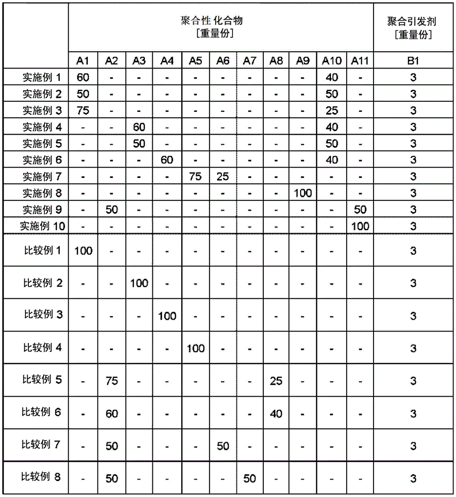
< A > polymerizable Compound
< A1> isobornyl acrylate (Kyoeisha Chemical Co., Ltd., product name: IB-XA, manufactured by Ltd.)
< A2> benzyl acrylate (Osaka Organic Chemical Industry Co., Ltd., product name: V #160 manufactured by Ltd.)
< A3> dicyclopentyl acrylate (Hitachi Chemical Co., Ltd., product name: FA-513AS, manufactured by Ltd.)
< A4> 2-naphthylmethyl acrylate (NARD institute, manufactured by Ltd.)
< A5> diphenylmethyl acrylate (NARD institute, manufactured by Ltd.)
< A6>1, 6-hexanediol diacrylate (Osaka Organic Chemical Industry Co., Ltd., product name: V #230 manufactured by Ltd.)
< A7>1, 10-decanediol diacrylate (Osaka Organic Chemical Industry Co., Ltd., product name: V #230, manufactured by Ltd.)
< A8> Dimethylol tricyclodecane diacrylate (KyoeishcA Chemical Co., Ltd., product name: DCP-A, manufactured by Ltd.)
< A9> Phenylethylene glycol diacrylate (manufactured by NARD institute, Ltd.)
< A10> m-xylylene diacrylate (NARD institute, manufactured by Ltd.)
< A11> 2-phenyl-1, 3-propanediol diacrylate (NARD institute, manufactured by Ltd.)
(B) (polymerization initiator)
< B1> Lucirin TPO (manufactured by BASF Japan Ltd.)
The composition of the photocurable composition for imprinting prepared using the above materials is shown in table 1 below. After preparation, filtration was performed using a 0.2 μm filter containing ultra-high molecular weight polyethylene.
TABLE 1
For the photocurable composition for imprinting shown in table 1 above, viscosity, glass transition temperature, and dry etching measurements were performed using the following procedures, and then the coefficient of thermal expansion, Ohnishi parameter, and etching rate were calculated.
(1. measurement of viscosity of photocurable composition for imprint)
The viscosity of the photocurable composition for imprint at 23 ℃ was measured using a cone-plate type rotational viscometer RE-85L (manufactured by Toki Sangyo Co., Ltd.).
(2. preparation of photocurable film for measurement of glass transition temperature of photocurable composition for imprinting)
Using a rheometer MCR301 with UV irradiation option manufactured by Anton Paar, 70 μ resist was dropped and filled into a100 μm gap between a rotating rod with a bottom surface having a diameter φ of 8.0mm and a quartz stage. The vertical reaction force (normal reaction) of the rotating rod was set to 0N so that the gap followed the curing and shrinkage of the photocurable composition.
Subsequently, the rotational vibration cycle of the rotary rod was set to 5Hz, and after the rotational vibration was started for 10 seconds, UV light irradiation was started from the quartz stage side. The exposure time was set at 600 seconds, the exposure wavelength was fixed at 365nm, and the illuminance was fixed at 1.0mW/cm2The temperature was fixed at 23 ℃.
(3. measurement of glass transition temperature and coefficient of thermal expansion of photocurable composition for imprint)
The loss tangent tan δ of the photocurable film prepared in (2) was measured while raising the temperature from 23 ℃ to 200 ℃ in a state where the vertical reaction force of the rotating rod was set to 0N so that the gap between the rotating rod and the quartz stage followed the thermal expansion and thermal contraction of the photocurable composition. The temperature rise rate was set to 4 ℃/min. The temperature at which tan δ reached the maximum was defined as the glass transition temperature. Further, the thermal expansion coefficient of the photo-curing film is calculated by the following expression (3).
Film thickness (. mu.m) of the photocurable film at 120 ℃ and film thickness (. mu.m) of the photocurable film at 23 ℃ were determined as thermal expansion coefficient (%) (3)
Here, the thickness of the photo-cured film is the gap between the spin bar and the quartz stage.
(4. calculation of Ohnishi parameter of photocurable composition for imprinting)
The Ohnishi parameter of the (A) component of the photocurable composition in the composition table shown in Table 1 was calculated using the following expression (2).
OP=n1OP1+n2OP2+……nnOPn (2)
(5. preparation of photo-cured film for dry etching of photo-curable composition for imprinting)
2.0. mu.L of the obtained photocurable composition for imprinting was dropped onto a silicon wafer on which a 60 nm-thick adhesion-promoting layer was formed as an adhesion layer, 1 mm-thick quartz glass was covered from the upper side, and then the region (25 mm. times.25 mm) was filled with the photocurable composition for imprinting.
Next, a UV light source with an ultra-high pressure mercury lamp was caused to emit light from above the quartz glass and passed through an interference filter described below, and then the coated film was irradiated through the quartz glass for 200 seconds. The interference filter used in the light irradiation was VPF-25C-10-15-31300(SIGMA KOKI Co., Ltd.). Ultraviolet light as irradiation light has a single wavelength of 313 + -5 nm and illuminance of 1mW/cm2。
After the light irradiation, the quartz glass was peeled off, and a photocurable film of the photocurable composition for imprinting having an average film thickness of 3.2 μm was obtained on a silicon wafer.
(6. measurement of etching Rate of photo-cured film for Dry etching of photo-curable composition for imprint)
NE-500 was manufactured by ULVAC, and the etching gas and the flow rate thereof were set to CF4/CHF3The photo-cured film prepared in (5) was subjected to dry etching for 500 seconds at 50sccm/50sccm, and then the film thickness decreased by the dry etching was measured to calculate a dry etching rate (nm/s). A lower etch rate indicates a higher resistance to dry etching.
The measurement results are shown in table 2 below. When the composition of comparative example 1 was set to 1, the dry etching rate ratio (DE rate ratio) was obtained as a percentage by calculating a relative value.
TABLE 2

From the results shown in table 2, it can be confirmed that the photocurable composition for imprints of the examples had small thermal expansion.
Considering that the thermal expansion coefficients in examples 1 to 8 are all lower than 10%, examples 1 to 8 are compositions in which the thermal expansion of the resist in dry etching is small. Further, examples 1 to 8 are compositions having excellent dry etching resistance in view of the DE rate ratio being equal to or higher than that of comparative example 1. The viscosity is 50 mPas or less, and the filling property is excellent. Considering that examples 9 and 10 have a DE rate ratio less than comparative example 1 and a viscosity of 50mPa · s or less, examples 9 and 10 are considered to be compositions having low thermal expansion similar to examples 1-8.
On the other hand, in comparative examples 1 to 3, the glass transition temperature was 90 ℃ or higher, but the thermal expansion coefficient was 10% or higher. This is considered to be because the proportion of the polyfunctional monomer is less than 20% by weight, that is, only the monofunctional acrylic monomer is contained, and thus the crosslinking density of comparative examples 1 to 3 is lower than that of the composition containing 20% by weight or more of the polyfunctional acrylic monomer as in examples 1 to 8. More specifically, it is considered that thermal deformation and thermal expansion easily occur in dry etching.
Comparative examples 5 to 8 are compositions containing 20% by weight or more of a polyfunctional monomer, but have a thermal expansion coefficient of 10% or more. This is considered to be because the glass transition temperature is low, and thus thermal deformation and thermal expansion easily occur in dry etching, similarly to comparative examples 1 to 4.
It can be confirmed that the compositions of examples 1 to 8 are photocurable compositions for imprinting having small thermal expansion, excellent dry etching resistance and excellent filling property due to the absence of the polyfunctional monomer.
Industrial applicability
As described above, the present invention can provide a photocurable composition for imprinting having small thermal expansion in dry etching and excellent filling property in a photoimprinting method. Further, the present invention can provide a method for producing the photocurable composition for imprinting, a method for producing a film, a method for producing an optical component, a method for producing a circuit board, and a method for producing an electronic component.
The present invention can provide a photocurable composition for imprinting having small thermal expansion in dry etching and excellent filling properties in a photoimprinting method. Further, the present invention can also provide a method for producing a film using the photocurable composition for imprinting, a method for producing an optical component using the photocurable composition for imprinting, a method for producing a circuit board using the photocurable composition for imprinting, and a method for producing an electronic component using the photocurable composition for imprinting.
While the present invention has been described with reference to exemplary embodiments, it is to be understood that the invention is not limited to the disclosed exemplary embodiments. The scope of the following claims is to be accorded the broadest interpretation so as to encompass all such modifications and equivalent structures and functions.
The present application claims the benefits of japanese patent application nos. 2014-257798, 2015-099486, filed 5-14, 2015, and 2015-232535, filed 11-28, 2015, filed 12-19, 2014, which are incorporated herein by reference in their entireties.
Claims (20)
1. A photocurable composition for imprinting, characterized by comprising at least:
a polymerizable compound (A); and
a photopolymerization initiator (B),
wherein the polymerizable compound (A) contains 20 wt% or more of a polyfunctional (meth) acrylic monomer and
a glass transition temperature of a photo-cured product of the photo-curable composition for imprinting is 90 ℃ or higher;
wherein the photocurable composition for imprinting has a glass transition temperature of 90 ℃ or higher is determined by: while the temperature was increased, the loss tangent tan δ of a film obtained by photocuring a photocurable composition for imprinting comprising 100 parts by weight of the polymerizable compound (a) and 3 parts by weight of Lucirin TPO as the photopolymerization initiator (B) was measured to find that the temperature at which tan δ reaches the maximum value was 90 ℃ or more.
2. A photocurable composition for imprinting, characterized by comprising at least:
a polymerizable compound (A); and
a photopolymerization initiator (B),
wherein the polymerizable compound (A) contains 20 wt% or more of a polyfunctional (meth) acrylic monomer and
a glass transition temperature of a photo-cured product of the photo-curable composition for imprinting is 90 ℃ or higher;
wherein the polymerizable compound (A) has an Ohnishi parameter of 3.2 or less.
3. A photocurable composition for imprinting, characterized by comprising at least:
a polymerizable compound (A); and
a photopolymerization initiator (B),
wherein the polymerizable compound (A) contains 20 wt% or more of a polyfunctional (meth) acrylic monomer and
a glass transition temperature of a photo-cured product of the photo-curable composition for imprinting is 90 ℃ or higher;
wherein a viscosity of a mixture of components excluding the solvent in the photocurable composition for imprinting at 23 ℃ is 5 mPas or more and 12 mPas or less.
4. The photocurable composition for imprinting according to claim 3, wherein the polymerizable compound (A) is a mixture of a monofunctional (meth) acrylic monomer and a polyfunctional (meth) acrylic monomer.
5. The photocurable composition for imprinting according to claim 3, wherein the polymerizable compound (A) comprises 25% by weight or more of a polyfunctional (meth) acrylic monomer.
6. The photocurable composition for imprinting according to claim 3, wherein the polymerizable compound (A) contains at least 40% by weight or more of a polyfunctional (meth) acrylic monomer, and a glass transition temperature of a photocured product of the photocurable composition for imprinting is 120 ℃ or more.
7. A photocurable composition for imprinting, characterized by comprising at least:
a polymerizable compound (A); and
a photopolymerization initiator (B),
wherein the polymerizable compound (A) contains 20 wt% or more of a polyfunctional (meth) acrylic monomer and
a glass transition temperature of a photo-cured product of the photo-curable composition for imprinting is 90 ℃ or higher;
wherein the polyfunctional acrylic monomer contained in the polymerizable compound (A) is any one of m-xylylene diacrylate, phenyl ethylene glycol diacrylate and 2-phenyl-1, 3-propanediol diacrylate.
8. A method of manufacturing a film having a pattern shape, the method comprising:
a step [1] of disposing the photocurable composition for imprinting according to any one of claims 1 to 7 on a substrate;
a step [2] of bringing the curable composition into contact with a mold having an original pattern for transferring a pattern shape;
a step [3] of aligning the substrate and the mold;
a step [4] of irradiating the curable composition with light to form a photocured film; and
and a step [5] of releasing the cured film and the mold from each other.
9. The method for producing a film having a pattern shape according to claim 8, comprising performing steps [1] - [5] twice or more for different regions on the substrate.
10. The method for manufacturing a film having a pattern shape according to claim 8, wherein a surface of an original pattern of the mold comprises quartz.
11. The method for producing a film having a pattern shape according to claim 8, wherein the step [2] is performed under an atmosphere containing a condensable gas.
12. The method for producing a film having a pattern shape according to claim 11, wherein the step [2] is performed under an atmosphere of a mixed gas of a condensable gas and a non-condensable gas.
13. The method for manufacturing a film having a pattern shape according to claim 12, wherein the non-condensable gas is helium.
14. The method for manufacturing a film having a pattern shape according to claim 11, wherein the condensable gas is 1,1,1,3, 3-pentafluoropropane.
15. A method of manufacturing an optical assembly, the method comprising:
a step of obtaining a film having a pattern shape by the manufacturing method according to any one of claims 8 to 14.
16. A method of manufacturing an optical assembly, the method comprising:
a step of obtaining a film having a pattern shape by the manufacturing method according to any one of claims 8 to 14; and a step of etching or ion implantation of the substrate using the pattern shape of the obtained film as a mask.
17. A method of manufacturing a circuit board, the method comprising:
a step of obtaining a film having a pattern shape by the manufacturing method according to any one of claims 8 to 14; and a step of etching or ion implantation of the substrate using the pattern shape of the obtained film as a mask.
18. A method of manufacturing an electronic assembly, the method comprising:
a step of obtaining a circuit board by the method for manufacturing a circuit board according to claim 17; and
a step of forming an electronic component on the circuit board.
19. A photocurable film for dry etching, which is used for dry etching, characterized in that the photocurable film is obtained by curing the photocurable composition for imprinting according to any one of claims 1 to 7.
20. A semiconductor substrate pretreated by dry etching, comprising:
a semiconductor substrate; and
the photo-curable film for etching according to claim 19 patterned on the semiconductor substrate.
Applications Claiming Priority (7)
| Application Number | Priority Date | Filing Date | Title |
|---|---|---|---|
| JP2014257798 | 2014-12-19 | ||
| JP2014-257798 | 2014-12-19 | ||
| JP2015099486A JP6624808B2 (en) | 2014-07-25 | 2015-05-14 | Photocurable composition, method for producing cured product pattern using the same, method for producing optical component, method for producing circuit board |
| JP2015-099486 | 2015-05-14 | ||
| JP2015232535A JP6324363B2 (en) | 2014-12-19 | 2015-11-28 | Photocurable composition for imprint, method for producing film using the same, method for producing optical component, method for producing circuit board, method for producing electronic component |
| JP2015-232535 | 2015-11-28 | ||
| PCT/JP2015/006244 WO2016098345A1 (en) | 2014-12-19 | 2015-12-15 | Photocurable composition for imprint, method for producing film using the same, method for producing optical component using the same, method for producing circuit board using the same, and method for producing electronic component using the same |
Publications (2)
| Publication Number | Publication Date |
|---|---|
| CN107112208A CN107112208A (en) | 2017-08-29 |
| CN107112208B true CN107112208B (en) | 2021-06-25 |
Family
ID=56242897
Family Applications (1)
| Application Number | Title | Priority Date | Filing Date |
|---|---|---|---|
| CN201580069521.5A Active CN107112208B (en) | 2014-12-19 | 2015-12-15 | Photocurable composition and its application |
Country Status (5)
| Country | Link |
|---|---|
| US (2) | US11003073B2 (en) |
| JP (3) | JP6324363B2 (en) |
| KR (3) | KR102246568B1 (en) |
| CN (1) | CN107112208B (en) |
| TW (1) | TWI596431B (en) |
Families Citing this family (12)
| Publication number | Priority date | Publication date | Assignee | Title |
|---|---|---|---|---|
| JP6837123B2 (en) * | 2017-02-24 | 2021-03-03 | シャープ株式会社 | Decorative film |
| CN110741463B (en) * | 2017-06-09 | 2024-02-20 | 三井化学株式会社 | Method for manufacturing substrate with fine uneven pattern, resin composition, and laminate |
| JP6550434B2 (en) * | 2017-09-29 | 2019-07-24 | シャープ株式会社 | Method for producing antifouling film |
| CN111796385A (en) * | 2019-04-08 | 2020-10-20 | 三营超精密光电(晋城)有限公司 | Optical lens, lens module using same and electronic device |
| US20200339828A1 (en) * | 2019-04-26 | 2020-10-29 | Canon Kabushiki Kaisha | Photocurable composition |
| EP4443202A4 (en) | 2021-12-24 | 2025-04-23 | Dexerials Corporation | METAL GRID POLARIZER, METHOD FOR MANUFACTURING METAL GRID POLARIZER, PROJECTION DISPLAY DEVICE, VEHICLE, AND PHOTOCURABLE ACRYLIC RESIN FOR PRINTING |
| JP2024090185A (en) | 2022-12-22 | 2024-07-04 | デクセリアルズ株式会社 | Photocurable acrylic resin for imprinting |
| JP2023125842A (en) * | 2022-02-28 | 2023-09-07 | キヤノン株式会社 | Pattern forming method and article manufacturing method |
| WO2024135835A1 (en) | 2022-12-22 | 2024-06-27 | デクセリアルズ株式会社 | Wire grid polarizing element, method for manufacturing wire grid polarizing element, projection display device, and vehicle |
| WO2024135836A1 (en) | 2022-12-22 | 2024-06-27 | デクセリアルズ株式会社 | Wire grid polarization element, method for producing wire grid polarization element, projection display device, and vehicle |
| US20240411225A1 (en) * | 2023-06-09 | 2024-12-12 | Canon Kabushiki Kaisha | System including heating means and actinic radiation source and a method of using the same |
| TWI863515B (en) * | 2023-08-18 | 2024-11-21 | 光群雷射科技股份有限公司 | Manufacturing method of embossing mask |
Citations (5)
| Publication number | Priority date | Publication date | Assignee | Title |
|---|---|---|---|---|
| CN1977221A (en) * | 2004-05-31 | 2007-06-06 | 富士胶片株式会社 | Pattern forming method, color filter manufacturing method, color filter, and liquid crystal display |
| CN101116035A (en) * | 2004-06-15 | 2008-01-30 | 富士胶片株式会社 | Photosensitive composition, pattern forming method, and permanent pattern |
| TW201038596A (en) * | 2009-03-09 | 2010-11-01 | Fujifilm Corp | Curable composition for imprint, patterning method and pattern |
| TW201424996A (en) * | 2012-09-13 | 2014-07-01 | Hitachi Chemical Co Ltd | Method of manufacturing resin layer having patterns, and resin composition applied in the same |
| TW201443000A (en) * | 2013-05-09 | 2014-11-16 | 佳能股份有限公司 | a compound, a photocurable composition, and a method of producing a patterned film, an optical component, a circuit board, an electronic component, and a cured product by using the photocurable composition |
Family Cites Families (42)
| Publication number | Priority date | Publication date | Assignee | Title |
|---|---|---|---|---|
| US4323636A (en) | 1971-04-01 | 1982-04-06 | E. I. Du Pont De Nemours And Company | Photosensitive block copolymer composition and elements |
| CA1099435A (en) | 1971-04-01 | 1981-04-14 | Gwendyline Y. Y. T. Chen | Photosensitive block copolymer composition and elements |
| US4423135A (en) | 1981-01-28 | 1983-12-27 | E. I. Du Pont De Nemours & Co. | Preparation of photosensitive block copolymer elements |
| US4414278A (en) | 1982-04-22 | 1983-11-08 | E. I. Du Pont De Nemours And Company | Crosslinked triacrylate polymer beads |
| JP2002200623A (en) * | 2000-10-26 | 2002-07-16 | Dainippon Ink & Chem Inc | Manufacturing method of resin composite |
| WO2007024323A2 (en) * | 2005-06-17 | 2007-03-01 | The University Of North Carolina At Chapel Hill | Nanoparticle fabrication methods, systems, and materials |
| JP4770354B2 (en) | 2005-09-20 | 2011-09-14 | 日立化成工業株式会社 | Photocurable resin composition and pattern forming method using the same |
| US7670530B2 (en) * | 2006-01-20 | 2010-03-02 | Molecular Imprints, Inc. | Patterning substrates employing multiple chucks |
| JP4929722B2 (en) | 2006-01-12 | 2012-05-09 | 日立化成工業株式会社 | Photo-curable nanoprint resist material and pattern formation method |
| JP5306903B2 (en) | 2008-07-02 | 2013-10-02 | 富士フイルム株式会社 | Curable composition for imprint, cured product using the same, method for producing the same, and member for liquid crystal display device |
| JP2010037541A (en) * | 2008-07-10 | 2010-02-18 | Fujifilm Corp | Curable composition for imprint, pattern forming method, and pattern |
| JP2010106062A (en) * | 2008-10-28 | 2010-05-13 | Fujifilm Corp | Composition for nanoimprint, and pattern and method for forming the same |
| KR101326497B1 (en) | 2008-12-01 | 2013-11-08 | 에이제이아이 가부시끼가이샤 | Method of molding |
| JP2010132762A (en) * | 2008-12-04 | 2010-06-17 | Nippon Paint Co Ltd | Method for producing photocurable resin composition and film having uneven surface |
| JP2011082347A (en) * | 2009-10-07 | 2011-04-21 | Fujifilm Corp | Curable composition for imprint, method of manufacturing cured product, and the cured product |
| JP5511415B2 (en) | 2010-02-02 | 2014-06-04 | 富士フイルム株式会社 | Curable composition for imprint, pattern forming method and pattern |
| US20110300367A1 (en) | 2010-06-07 | 2011-12-08 | Ching-Kee Chien | Optical Fiber With Photoacid Coating |
| JP2012072269A (en) | 2010-09-28 | 2012-04-12 | Fujifilm Corp | Microstructure |
| JP2012227190A (en) * | 2011-04-15 | 2012-11-15 | Nippon Shokubai Co Ltd | Curable resin composition for nanoimprint |
| JP5829177B2 (en) * | 2011-07-12 | 2015-12-09 | 富士フイルム株式会社 | Curable composition for imprint, pattern forming method and pattern |
| JP5710553B2 (en) * | 2011-08-25 | 2015-04-30 | 富士フイルム株式会社 | Curable composition for imprint, pattern forming method and pattern |
| JP2013065813A (en) | 2011-08-29 | 2013-04-11 | Fujifilm Corp | Imprint system and maintenance method of the same |
| JP5806903B2 (en) * | 2011-09-30 | 2015-11-10 | 富士フイルム株式会社 | Nanoimprint method and resist composition used therefor |
| JP5767615B2 (en) * | 2011-10-07 | 2015-08-19 | 富士フイルム株式会社 | Underlayer film composition for imprint and pattern forming method using the same |
| JP6108765B2 (en) | 2011-12-19 | 2017-04-05 | キヤノン株式会社 | Photocurable composition and pattern forming method |
| JP5838826B2 (en) | 2012-01-23 | 2016-01-06 | 大日本印刷株式会社 | Pattern structure manufacturing method, nanoimprint lithography method, and imprint apparatus |
| JP2013170227A (en) * | 2012-02-21 | 2013-09-02 | Fujifilm Corp | Photopolymerizable composition |
| JP5846974B2 (en) * | 2012-03-13 | 2016-01-20 | 富士フイルム株式会社 | Curable composition for photoimprint, pattern forming method and pattern |
| JP5930832B2 (en) | 2012-04-27 | 2016-06-08 | キヤノン株式会社 | Method for producing photocured product |
| JP2014074165A (en) * | 2012-09-12 | 2014-04-24 | Sanyo Chem Ind Ltd | Photosensitive composition |
| JP6278645B2 (en) | 2012-09-24 | 2018-02-14 | キヤノン株式会社 | Photocurable composition and method for producing film using the same |
| TWI589994B (en) * | 2012-10-09 | 2017-07-01 | 佳能股份有限公司 | Photocurable composition and method of manufacturing the same |
| CN102911052B (en) | 2012-10-13 | 2015-03-25 | 江苏和成显示科技股份有限公司 | Polymerized star compound and polymerized product and application thereof in liquid crystal device |
| JP6058371B2 (en) * | 2012-12-07 | 2017-01-11 | 日本合成化学工業株式会社 | Manufacturing method of plastic sheet for display |
| CN103113900B (en) | 2013-02-01 | 2015-02-04 | 江苏和成显示科技股份有限公司 | Polymer stabilized alignment type liquid crystal composition and application thereof |
| JP6080813B2 (en) | 2013-08-30 | 2017-02-15 | キヤノン株式会社 | Composition for optical imprint, film manufacturing method, optical component manufacturing method, circuit board manufacturing method, and electronic component manufacturing method using the same |
| JP6460672B2 (en) | 2013-09-18 | 2019-01-30 | キヤノン株式会社 | Film manufacturing method, optical component manufacturing method, circuit board manufacturing method, and electronic component manufacturing method |
| CN106164112B (en) * | 2014-03-27 | 2018-02-06 | 瓦克化学公司 | The adhesive of paper coating compositions |
| JP6643802B2 (en) * | 2014-05-09 | 2020-02-12 | キヤノン株式会社 | Curable composition, cured product thereof, method for producing cured product, method for producing optical component, method for producing circuit board, and method for producing electronic component |
| JP6424481B2 (en) * | 2014-06-11 | 2018-11-21 | 中西金属工業株式会社 | Magnetic encoder and method of manufacturing the same |
| JP6779611B2 (en) * | 2014-12-19 | 2020-11-04 | キヤノン株式会社 | Photocurable composition for imprint, manufacturing method of cured film, manufacturing method of optical component, manufacturing method of circuit board, manufacturing method of electronic component |
| US11820165B2 (en) * | 2018-03-30 | 2023-11-21 | Dai Nippon Toryo Co., Ltd. | Printed object |
-
2015
- 2015-11-28 JP JP2015232535A patent/JP6324363B2/en active Active
- 2015-12-15 KR KR1020197037480A patent/KR102246568B1/en active Active
- 2015-12-15 KR KR1020197016193A patent/KR102059314B1/en active Active
- 2015-12-15 US US15/537,320 patent/US11003073B2/en active Active
- 2015-12-15 KR KR1020177019229A patent/KR101988782B1/en active Active
- 2015-12-15 CN CN201580069521.5A patent/CN107112208B/en active Active
- 2015-12-18 TW TW104142771A patent/TWI596431B/en active
-
2018
- 2018-04-12 JP JP2018076976A patent/JP2018125559A/en active Pending
-
2019
- 2019-12-16 JP JP2019226322A patent/JP6907293B2/en active Active
-
2021
- 2021-04-01 US US17/220,759 patent/US20210223690A1/en active Pending
Patent Citations (5)
| Publication number | Priority date | Publication date | Assignee | Title |
|---|---|---|---|---|
| CN1977221A (en) * | 2004-05-31 | 2007-06-06 | 富士胶片株式会社 | Pattern forming method, color filter manufacturing method, color filter, and liquid crystal display |
| CN101116035A (en) * | 2004-06-15 | 2008-01-30 | 富士胶片株式会社 | Photosensitive composition, pattern forming method, and permanent pattern |
| TW201038596A (en) * | 2009-03-09 | 2010-11-01 | Fujifilm Corp | Curable composition for imprint, patterning method and pattern |
| TW201424996A (en) * | 2012-09-13 | 2014-07-01 | Hitachi Chemical Co Ltd | Method of manufacturing resin layer having patterns, and resin composition applied in the same |
| TW201443000A (en) * | 2013-05-09 | 2014-11-16 | 佳能股份有限公司 | a compound, a photocurable composition, and a method of producing a patterned film, an optical component, a circuit board, an electronic component, and a cured product by using the photocurable composition |
Also Published As
| Publication number | Publication date |
|---|---|
| JP6907293B2 (en) | 2021-07-21 |
| JP2020039008A (en) | 2020-03-12 |
| KR20190142450A (en) | 2019-12-26 |
| KR20190067264A (en) | 2019-06-14 |
| US20210223690A1 (en) | 2021-07-22 |
| TWI596431B (en) | 2017-08-21 |
| JP2016117885A (en) | 2016-06-30 |
| KR20170094386A (en) | 2017-08-17 |
| KR102059314B1 (en) | 2020-02-11 |
| KR102246568B1 (en) | 2021-04-30 |
| CN107112208A (en) | 2017-08-29 |
| US11003073B2 (en) | 2021-05-11 |
| JP6324363B2 (en) | 2018-05-16 |
| US20170351172A1 (en) | 2017-12-07 |
| KR101988782B1 (en) | 2019-06-12 |
| TW201624122A (en) | 2016-07-01 |
| JP2018125559A (en) | 2018-08-09 |
Similar Documents
| Publication | Publication Date | Title |
|---|---|---|
| CN107112208B (en) | Photocurable composition and its application | |
| TWI632047B (en) | Pattern forming method, method of manufacturing processed substrate, method of manufacturing optical element, method of manufacturing circuit board, method of manufacturing electronic component, and method of manufacturing transfer die | |
| CN108885976B (en) | Pattern forming method, production method of processed substrate, production method of optical part, production method of circuit board, production method of electronic part, and production method of imprint mold | |
| CN109075033B (en) | Pattern forming method, method for manufacturing processed substrate, method for manufacturing optical module, method for manufacturing circuit substrate, method for manufacturing electronic module, and method for manufacturing imprint mold | |
| CN105659358B (en) | Film, optical component, circuit board and electronic component production method and composition | |
| CN108602238B (en) | Pattern forming method, production method of processed substrate, production method of optical component, production method of circuit substrate, production method of electronic component, and production method of imprint mold | |
| CN110392919B (en) | Pattern forming method and fabrication method of processing substrate, optical component and quartz mold replica and coating material for imprint pretreatment and combination with imprint resist | |
| CN107251192B (en) | Patterning method, production method of processed substrate, production method of optical component, production method of circuit board, and production method of electronic component | |
| KR102045700B1 (en) | Curable composition and cured product thereof, method for producing cured product, method for manufacturing optical component, method for manufacturing circuit board, and method for manufacturing electronic component | |
| CN106574007B (en) | Photocurable composition, method for producing pattern of cured product using same, method for producing optical component, and method for producing circuit board | |
| TWI584068B (en) | Photocurable composition, and method for forming cured product pattern and manufacturing optical component, circuit board and imprinting mold using the same | |
| WO2016098345A1 (en) | Photocurable composition for imprint, method for producing film using the same, method for producing optical component using the same, method for producing circuit board using the same, and method for producing electronic component using the same | |
| CN107112209A (en) | Photocurable composition for imprinting, production method of cured film, production method of optical component, production method of circuit board and production method of electronic component |
Legal Events
| Date | Code | Title | Description |
|---|---|---|---|
| PB01 | Publication | ||
| PB01 | Publication | ||
| SE01 | Entry into force of request for substantive examination | ||
| SE01 | Entry into force of request for substantive examination | ||
| GR01 | Patent grant | ||
| GR01 | Patent grant |