CN107046091B - Light-emitting device with light shape adjusting structure and manufacturing method thereof - Google Patents
Light-emitting device with light shape adjusting structure and manufacturing method thereof Download PDFInfo
- Publication number
- CN107046091B CN107046091B CN201610082142.6A CN201610082142A CN107046091B CN 107046091 B CN107046091 B CN 107046091B CN 201610082142 A CN201610082142 A CN 201610082142A CN 107046091 B CN107046091 B CN 107046091B
- Authority
- CN
- China
- Prior art keywords
- light
- shape adjusting
- adjusting structure
- led chip
- emitting device
- Prior art date
- Legal status (The legal status is an assumption and is not a legal conclusion. Google has not performed a legal analysis and makes no representation as to the accuracy of the status listed.)
- Active
Links
Images


Classifications
-
- H—ELECTRICITY
- H10—SEMICONDUCTOR DEVICES; ELECTRIC SOLID-STATE DEVICES NOT OTHERWISE PROVIDED FOR
- H10H—INORGANIC LIGHT-EMITTING SEMICONDUCTOR DEVICES HAVING POTENTIAL BARRIERS
- H10H20/00—Individual inorganic light-emitting semiconductor devices having potential barriers, e.g. light-emitting diodes [LED]
- H10H20/80—Constructional details
- H10H20/85—Packages
- H10H20/855—Optical field-shaping means, e.g. lenses
-
- H—ELECTRICITY
- H10—SEMICONDUCTOR DEVICES; ELECTRIC SOLID-STATE DEVICES NOT OTHERWISE PROVIDED FOR
- H10H—INORGANIC LIGHT-EMITTING SEMICONDUCTOR DEVICES HAVING POTENTIAL BARRIERS
- H10H20/00—Individual inorganic light-emitting semiconductor devices having potential barriers, e.g. light-emitting diodes [LED]
- H10H20/80—Constructional details
- H10H20/85—Packages
- H10H20/851—Wavelength conversion means
-
- H10W90/00—
-
- H10W72/0198—
Landscapes
- Led Device Packages (AREA)
Abstract
本发明是揭露一芯片级封装发光装置及其制造方法,该发光装置包含覆晶式LED芯片及光形调整结构以形成单色光发光装置,其亦可更包含设置于LED芯片上的荧光结构以形成白光发光装置。其中,本发明所揭露的光形调整结构是由重量百分比不大于30%的光散射性微粒混合于高分子材料中所形成,并设置于发光装置的侧部、或设置于发光装置的上部。借此,光形调整结构可因光学散射特性而使部分光线改变其传递路径,设置于发光装置的侧部时,可减少侧向射出的光线,而设置于发光装置的上部时,可减少正向射出的光线,故而可调整发光装置的光形与发光角度。
The present invention discloses a chip-level packaged light-emitting device and a method for manufacturing the same. The light-emitting device includes a flip-chip LED chip and a light shape adjustment structure to form a monochromatic light-emitting device. It may also include a fluorescent structure disposed on the LED chip to form a white light-emitting device. The light shape adjustment structure disclosed in the present invention is formed by mixing light-scattering particles with a weight percentage not greater than 30% in a polymer material, and is disposed on the side of the light-emitting device, or on the top of the light-emitting device. Thus, the light shape adjustment structure can change the transmission path of part of the light due to the optical scattering characteristics. When disposed on the side of the light-emitting device, the light emitted in the side direction can be reduced, and when disposed on the top of the light-emitting device, the light emitted in the forward direction can be reduced, so that the light shape and light-emitting angle of the light-emitting device can be adjusted.
Description
技术领域technical field
本发明有关一种发光装置及其制造方法,特别关于一种具有光形调整结构的芯片级封装发光装置及其制造方法。The present invention relates to a light-emitting device and a manufacturing method thereof, in particular to a chip-level packaged light-emitting device with a light shape adjustment structure and a manufacturing method thereof.
背景技术Background technique
随着LED技术的演进,芯片级封装(chip scale packaging,CSP)发光装置以其明显的优势于近年开始受到广大的重视。以最广泛被使用的白光CSP发光装置为例,如图1A所示,先前技术所揭露的白光CSP发光装置是由一覆晶式LED芯片71与一包覆LED芯片的荧光结构72所组成,其荧光结构72覆盖LED芯片71的上表面与四个立面,故CSP发光装置可从其顶面及四个侧面发出光线,即由不同方向的五个面发出光线(五面发光)。With the evolution of LED technology, chip scale packaging (CSP) light-emitting devices have begun to receive widespread attention in recent years due to their obvious advantages. Taking the most widely used white light CSP light emitting device as an example, as shown in FIG. 1A , the white light CSP light emitting device disclosed in the prior art is composed of a flip
相较于传统支架型(PLCC-type)LED,CSP发光装置具有以下优点:(1)不需要金线及额外的支架,因此可明显节省材料成本;(2)因省略了支架,可进一步降低LED芯片与散热板之间的热阻,因此在相同操作条件下将具有较低的操作温度,或进而增加操作功率;(3)较低的操作温度可使LED芯片具有较高的芯片量子转换效率;(4)大幅缩小的封装尺寸使得在设计模块或灯具时,具有更大的设计弹性;(5)具有小发光面积,因此可缩小光展量(Etendue),使得二次光学更容易设计,亦或借此获得高发光强度(intensity)。Compared with the traditional bracket-type (PLCC-type) LED, the CSP light-emitting device has the following advantages: (1) No gold wires and additional brackets are required, so the material cost can be significantly saved; (2) The bracket is omitted, which can further reduce the cost. The thermal resistance between the LED chip and the heat dissipation plate, so it will have a lower operating temperature under the same operating conditions, or further increase the operating power; (3) The lower operating temperature can make the LED chip have a higher chip quantum conversion Efficiency; (4) The greatly reduced package size enables greater design flexibility when designing modules or lamps; (5) It has a small light-emitting area, so the etendue can be reduced, making secondary optics easier to design , or to obtain high luminous intensity (intensity).
CSP发光装置具有诸多优点,然而先前技术所揭露的CSP发光装置为五面发光,因此具有较大的发光角度,依CSP发光装置的不同尺寸比例,其发光角度约介于140度至160度之间,远大于传统支架型LED的发光角度(约120度)。虽大发光角度的CSP发光装置于部分应用具有其优势,但较大的发光角度却不适合于需小发光角度的光源的应用,例如,侧向式背光模块或投射灯等应用皆需采用具有小发光角度的光源以提升光线在传递上的能量利用效率(光源运用得光率),因此,CSP发光装置需进一步具有较小的发光角度才能满足此类应用需求。The CSP light-emitting device has many advantages. However, the CSP light-emitting device disclosed in the prior art is five-sided, so it has a large light-emitting angle. According to the different size ratios of the CSP light-emitting device, the light-emitting angle is about 140 degrees to 160 degrees. It is much larger than the light-emitting angle of traditional bracket-type LEDs (about 120 degrees). Although the CSP light-emitting device with a large light-emitting angle has its advantages in some applications, the large light-emitting angle is not suitable for the application of a light source with a small light-emitting angle. A light source with a small light-emitting angle can improve the energy utilization efficiency of light transmission (the rate of light used by the light source). Therefore, the CSP light-emitting device needs to have a smaller light-emitting angle to meet the needs of such applications.
虽然传统上可于LED封装体上制作一次光学透镜,使光形可进一步聚集,以得到所需的小发光角度。然而,对于尺寸大幅缩小的CSP发光装置而言,其在有限的空间内并不适合设置一次光学透镜,此举除了会大幅增加生产成本,亦会明显增加CSP发光装置的外形尺寸而失去其小尺寸的优势。Although traditionally, an optical lens can be fabricated on the LED package once, so that the light shape can be further concentrated, so as to obtain the required small light emission angle. However, for a CSP light-emitting device with a greatly reduced size, it is not suitable to install an optical lens in a limited space. This will not only greatly increase the production cost, but also significantly increase the overall size of the CSP light-emitting device and lose its small size. size advantage.
又,如图1B所示,其为另一种先前技术所揭露的顶面发光CSP发光装置,可提供较小的发光角度。该CSP发光装置是由一覆晶式LED芯片71、一荧光结构72及一反射结构73所构成,荧光结构72覆盖LED芯片71的上表面,而反射结构73包覆该LED芯片71的四个立面,在这样的结构下,CSP发光装置仅能从其顶面发出光线(顶面发光),因此整体上可具有较小的发光角度,其发光角度介于120度至130度之间。然而,如图1C所示,该顶面发光CSP发光装置的反射结构73是由高浓度的光散射性微粒混合于高分子材料中所形成,通常光散射性微粒的重量百分比浓度需大于30%,以达到将光线反射的效用,但部分光子(例如路径P)会于反射结构73内过度损耗(dissipation),例如光子于反射结构73内P’(光子路径终点)处被吸收,故导致了其因光子损耗而使封装体发光效率下降;又,于制作上,需要另一道制程将反射材料覆盖LED芯片的四个立面,这使制程变得更为复杂;若需进一步使用精密模具(mold)以更准确地控制反射结构的制程时,亦会明显增加生产成本。Also, as shown in FIG. 1B , it is another top-surface light-emitting CSP light-emitting device disclosed in the prior art, which can provide a smaller light-emitting angle. The CSP light-emitting device is composed of a flip-
有鉴于此,如何提供一制程简易、低生产成本及不增加外形尺寸的技术方案,并能避免光子于封装体内被吸收而过度损耗的情况下,来调整先前技术所揭露的CSP发光装置的发光角度或光形,使其缩小发光角度,甚至进一步增加发光角度,以符合不同应用所需,是可有效解决CSP发光装置目前于应用上所遭遇的问题。In view of this, how to provide a technical solution with simple process, low production cost and no increase in external size, and can avoid excessive loss due to absorption of photons in the package, so as to adjust the light emission of the CSP light-emitting device disclosed in the prior art It can effectively solve the problems encountered in the application of CSP light-emitting devices at present, by reducing the angle or light shape to reduce the light-emitting angle or even further increase the light-emitting angle to meet the needs of different applications.
发明内容SUMMARY OF THE INVENTION
本发明的一目的在于提供一种芯片级封装(chip scale packaging,CSP)发光装置及其制造方法,该发光装置具有简易制程与低生产成本,可于不增加先前技术所揭露的CSP发光装置外形尺寸的下具有小发光角度(如120度至140度),亦可借由设计不同的光形调整结构(beam shaping structure)而增加本发明所揭露的CSP发光装置的发光角度(如160度至170度),以满足更多的应用需求。One object of the present invention is to provide a chip scale packaging (CSP) light emitting device and a manufacturing method thereof. The light emitting device has a simple manufacturing process and low production cost, and can not increase the shape of the CSP light emitting device disclosed in the prior art. It has a small light-emitting angle (such as 120 degrees to 140 degrees) under the size, and can also increase the light-emitting angle of the CSP light-emitting device disclosed in the present invention by designing different beam shaping structures (such as 160 degrees to 160 degrees to 140 degrees). 170 degrees) to meet more application requirements.
为达上述目的,本发明所揭露的一种小发光角度CSP发光装置,其包含一覆晶式LED芯片、一荧光结构及一光形调整结构。覆晶式LED芯片具有一上表面、一下表面、一立面及一电极组;荧光结构形成于LED芯片的上表面与立面上;光形调整结构覆盖该荧光结构的侧部;该光形调整结构包含一高分子材料及一光散射性微粒,该光散射性微粒分布于该高分子材料中,且该光散射性微粒在该光形调整结构中的一重量百分比为相对低浓度,且不大于30%,如此可避免光子于光形调整结构内过度损耗(dissipation),并使部分光线散射至其他方向而减少发光角度。In order to achieve the above object, the present invention discloses a small light-emitting angle CSP light-emitting device, which includes a flip-chip LED chip, a fluorescent structure and a light shape adjustment structure. The flip-chip LED chip has an upper surface, a lower surface, a vertical surface and an electrode group; the fluorescent structure is formed on the upper surface and the vertical surface of the LED chip; the light shape adjustment structure covers the side of the fluorescent structure; the light shape The adjustment structure includes a polymer material and a light scattering particle, the light scattering particle is distributed in the polymer material, and a weight percentage of the light scattering particle in the light shape adjustment structure is relatively low concentration, and It is not more than 30%, which can avoid excessive dissipation of photons in the light shape adjustment structure, and make part of the light scatter to other directions to reduce the emission angle.
为达上述目的,本发明另揭露一种大发光角度CSP发光装置,其包含一LED芯片、一荧光结构、一透光结构以及一光形调整结构。LED芯片具有一上表面、一立面及一电极组;荧光结构形成于该LED芯片的上表面与立面上;透光结构形成于该荧光结构上;光形调整结构覆盖该透光结构的一顶面,该光形调整结构包含一高分子材料及一光散射性微粒,该光散射性微粒分布于该高分子材料中,且该光散射性微粒在该光形调整结构中的一重量百分比为相对低浓度,且不大于30%,如此可避免光子于光形调整结构内过度损耗(dissipation),并使部分光线散射至其他方向而增加发光角度。In order to achieve the above objective, the present invention further discloses a large light-emitting angle CSP light-emitting device, which includes an LED chip, a fluorescent structure, a light-transmitting structure and a light-shape adjustment structure. The LED chip has an upper surface, a vertical surface and an electrode group; a fluorescent structure is formed on the upper surface and the vertical surface of the LED chip; a light-transmitting structure is formed on the fluorescent structure; a top surface, the light shape adjustment structure includes a polymer material and a light scattering particle, the light scattering particle is distributed in the polymer material, and a weight of the light scattering particle in the light shape adjustment structure The percentage is relatively low and not more than 30%, so that excessive dissipation of photons in the light shape adjustment structure can be avoided, and part of the light can be scattered to other directions to increase the luminous angle.
为达上述目的,本发明又揭露一种小发光角度的单色光CSP发光装置,其包含一LED芯片及一光形调整结构。LED芯片具有一上表面、一立面及一电极组;光形调整结构至少覆盖该立面,该光形调整结构包含一高分子材料及一光散射性微粒,该光散射性微粒分布于该高分子材料中,且该光散射性微粒在该光形调整结构中的一重量百分比为相对低浓度,且不大于30%,如此可避免光子于光形调整结构内过度损耗(dissipation),并使部分光线散射至其他方向而减少发光角度。In order to achieve the above object, the present invention further discloses a monochromatic light CSP light-emitting device with a small light-emitting angle, which includes an LED chip and a light shape adjustment structure. The LED chip has an upper surface, a façade and an electrode set; the light shape adjustment structure covers at least the façade, the light shape adjustment structure includes a polymer material and a light scattering particle, and the light scattering particle is distributed in the In the polymer material, and a weight percentage of the light scattering particles in the light shape adjustment structure is relatively low, and not greater than 30%, so that excessive loss of photons in the light shape adjustment structure can be avoided (dissipation), and Scatters some of the light in other directions to reduce the beam angle.
为达上述目的,本发明再揭露一种发光装置的制造方法,其包含以下步骤:放置多个LED芯片于一离形材料上,以形成一LED芯片阵列;形成多个封装构造于该多个LED芯片上,该多个封装构造彼此相连;以及切割该多个封装构造。在切割该多个封装构造之前或之后,可移除该离形材料。In order to achieve the above object, the present invention further discloses a manufacturing method of a light-emitting device, which comprises the following steps: placing a plurality of LED chips on a release material to form an LED chip array; forming a plurality of packaging structures on the plurality of On the LED chip, the plurality of package structures are connected to each other; and the plurality of package structures are diced. The release material may be removed before or after dicing the plurality of package structures.
借此,本发明所揭露的发光装置及其制造方法能至少提供以下的有益效果:发光装置的光形调整结构是具有较低浓度的光散射性微粒(重量百分比不大于30%),当光线通过光形调整结构时,可使部分光线散射至其他方向,并使原光传递方向的光线强度衰减,同时亦可降低光子于光形调整结构内的损耗(dissipation),故可提升整体的发光效率。Therefore, the light-emitting device and the manufacturing method thereof disclosed in the present invention can at least provide the following beneficial effects: the light-shape adjustment structure of the light-emitting device has a relatively low concentration of light-scattering particles (not more than 30% by weight), when the light When the light shape adjustment structure is used, part of the light can be scattered to other directions, and the light intensity in the original light transmission direction can be attenuated, and the dissipation of photons in the light shape adjustment structure can also be reduced, so the overall light emission can be improved. efficiency.
因此,当光形调整结构被设置于本发明所揭露的发光装置的侧部时,从LED芯片立面方向(例如水平方向)所射出的光线在通过光形调整结构的过程中,会有一部分被散射至其他方向,而另一部分则维持原方向(或接近原方向)前进;如此,从发光装置的侧部(例如水平方向)射出的光线将会减少,而从发光装置的顶部(例如垂直方向)射出的光线则会增加,使得整体上的发光角度减小,借此,本发明所揭露的发光装置可具有小发光角度(例如可减小至120度至140度)。Therefore, when the light shape adjustment structure is disposed on the side of the light-emitting device disclosed in the present invention, a part of the light emitted from the vertical direction of the LED chip (for example, the horizontal direction) will pass through the light shape adjustment structure. is scattered in other directions, while the other part remains in the original direction (or close to the original direction); in this way, the light emitted from the side of the light-emitting device (such as the horizontal direction) will be reduced, and the light from the top of the light-emitting device (such as the vertical direction) will be reduced. direction) the emitted light will increase, so that the overall light-emitting angle decreases, whereby the light-emitting device disclosed in the present invention can have a small light-emitting angle (for example, can be reduced to 120 degrees to 140 degrees).
又,当本发明所揭露的光形调整结构被设置于LED芯片的上方,并与LED芯片的上表面保持一距离时,可使从发光装置的顶部(例如垂直方向)射出的光线衰减,使从发光装置的侧部(例如水平方向)射出的光线增加,因而使得整体上的发光角度增加(例如可增加至160度至170度)。In addition, when the light shape adjustment structure disclosed in the present invention is disposed above the LED chip and keeps a distance from the upper surface of the LED chip, the light emitted from the top of the light-emitting device (for example, in the vertical direction) can be attenuated, so that the The light emitted from the side portion (eg, horizontal direction) of the light-emitting device increases, so that the overall light-emitting angle increases (for example, it can be increased to 160 to 170 degrees).
此外,本发明所揭露的光形调整结构具有制程简易、容易控制与制作成本低廉的特性,且可容易地制作于CSP发光装置内而不增加其外形尺寸,因此适合应用于CSP发光装置的发光角度的调整。In addition, the light shape adjusting structure disclosed in the present invention has the characteristics of simple manufacturing process, easy control and low manufacturing cost, and can be easily manufactured in the CSP light emitting device without increasing its external size, so it is suitable for the light emitting of the CSP light emitting device Angle adjustment.
为让上述目的、技术特征及优点能更明显易懂,下文是以较佳的实施例配合所附图式进行详细说明。In order to make the above objects, technical features and advantages more clearly understood, the following describes the preferred embodiments in detail with the accompanying drawings.
附图说明Description of drawings
图1A及图1B分别为先前技术所揭露的发光装置全剖视图;1A and FIG. 1B are full cross-sectional views of a light-emitting device disclosed in the prior art, respectively;
图1C为图1B所示的发光装置的光线示意图;FIG. 1C is a schematic diagram of light of the light-emitting device shown in FIG. 1B;
图2A及图2B分别为依据本发明的第1较佳实施例的发光装置的立体图及全剖视图;2A and 2B are a perspective view and a full cross-sectional view of the light-emitting device according to the first preferred embodiment of the present invention, respectively;
图2C为图2B所示的发光装置的光线示意图;FIG. 2C is a schematic diagram of light of the light-emitting device shown in FIG. 2B;
图3A及图3B分别为图2B所示的发光装置的其他态样的示意图;3A and 3B are schematic diagrams of other aspects of the light-emitting device shown in FIG. 2B, respectively;
图4为依据本发明的第2较佳实施例的发光装置的全剖视图;4 is a full cross-sectional view of a light-emitting device according to a second preferred embodiment of the present invention;
图5为依据本发明的第3较佳实施例的发光装置的全剖视图;5 is a full cross-sectional view of a light-emitting device according to a third preferred embodiment of the present invention;
图6为依据本发明的第4较佳实施例的发光装置的全剖视图;6 is a full cross-sectional view of a light-emitting device according to a fourth preferred embodiment of the present invention;
图7A及图7B分别为依据本发明的第5较佳实施例的发光装置的立体图及全剖视图;以及7A and 7B are a perspective view and a full cross-sectional view of a light-emitting device according to a fifth preferred embodiment of the present invention, respectively; and
图8A至图9B分别为依据本发明的较佳实施例的发光装置的制造方法的步骤的示意图。8A to 9B are schematic diagrams of steps of a manufacturing method of a light-emitting device according to a preferred embodiment of the present invention, respectively.
符号说明Symbol Description
1A、1B、1C、1D、1E 发光装置1A, 1B, 1C, 1D, 1E Light-emitting device
100 LED芯片阵列100 LED chip array
10 LED芯片10 LED chips
11 上表面11 Top surface
12 下表面12 Lower surface
13 立面13 Facade
14 电极组14 Electrode set
200 封装构造200 Package structure
20 荧光结构20 Fluorescence structure
21 顶部21 top
211 顶面211 Top surface
22 侧部22 side
221 侧面221 Side
222 底面222 Bottom
23 延伸部23 Extensions
231 顶面231 Top surface
30、30’ 光形调整结构、BSS30, 30’ light shape adjustment structure, BSS
301 高分子材料301 Polymer materials
302 光散射性微粒302 Light Scattering Particles
31 顶面31 Top surface
32 侧面32 side
33 底面33 Bottom
40、40’ 透光结构40, 40' light transmission structure
41 顶面41 Top surface
50 柔性缓冲结构50 Flexible buffer structure
71 LED芯片71 LED chip
72 荧光结构72 Fluorescence structure
73 反射结构73 Reflective structure
900 离形材料900 Release material
D1 垂直方向D1 vertical direction
D2 水平方向D2 horizontal direction
L、L1、L2 光线L, L1, L2 rays
W 第一特征尺寸、特征尺寸W First feature size, feature size
T 第二特征尺寸、特征尺寸T Second feature size, feature size
P 光子路径P photon path
P’ 光子路径终点P’ is the end point of the photon path
具体实施方式Detailed ways
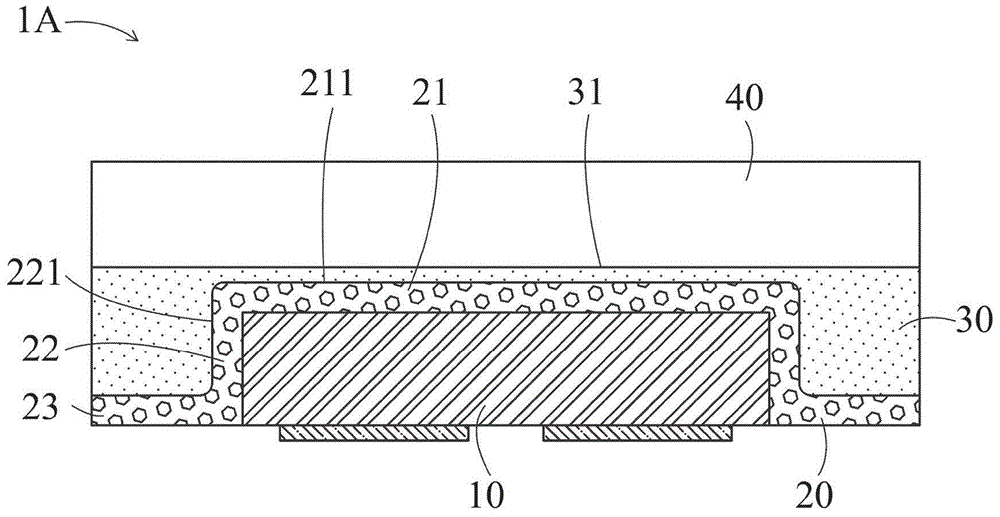
请参阅图2A及2B所示,其为依据本发明的第1较佳实施例的发光装置1A的立体图及全剖视图。发光装置1A可包含一LED芯片10、一荧光结构20、一光形调整结构(beamshaping structure,或可简称为BSS)30及一透光结构40,而荧光结构20、BSS 30及透光结构40又可构成可透光的一封装构造200;该多个元件的技术内容将依序说明如下。Please refer to FIGS. 2A and 2B , which are a perspective view and a full cross-sectional view of a light-emitting
LED芯片10为一覆晶式LED芯片,其包含一上表面11、一下表面12、一立面13及一电极组14。上表面11与下表面12为相对且相反地设置,而立面13形成于上表面11与下表面12之间、且连接上表面11与下表面12。换言之,立面13是沿着上表面11的边缘与下表面12的边缘而形成,故立面13相对于上表面11与下表面12为环形(例如矩型环)。The
电极组14设置于下表面12上,且可具有二个以上的电极。电能(图未示)可透过电极组14供应至LED芯片10内,以使LED芯片10发出光线。由于可产生光线的发光层(图未示)通常接近LED芯片10内部的下方,发光层所产生的光线会穿透LED芯片10的上表面11与立面13而向外传递。换言之,光线至少可从朝向不同方向的五个面射出。The
荧光结构20可改变「从LED芯片10的上表面11及立面13所发出」的光线的波长。也就是,LED芯片10所发出的光线(例如为蓝光)在通过荧光结构20时,一部分的光线接触到荧光结构20的荧光材料而被转换波长(例如变为黄光),而另一部分的光线未有接触到荧光材料而维持其既有波长;两部分的光线之后相混合而形成具有所需颜色的光束(例如为白光)。The
结构上,荧光结构20可包含一顶部21、一侧部22及一延伸部23,顶部21形成且覆盖于LED芯片10的上表面11上,可改变上表面11所射出的光线的波长;而侧部22形成且覆盖于LED芯片10的立面13上,可改变立面13所射出的光线的波长;延伸部23则是自侧部22向外延伸(即朝向远离立面13的方向延伸)。侧部22及延伸部23皆呈环状,围绕该LED芯片10;延伸部23的厚度可小于芯片10的厚度。Structurally, the
此外,顶部21具有一顶面211,其沿着一垂直方向D1(即LED芯片10的厚度方向)与LED芯片10的上表面11相距;侧部22具有一侧面221,其沿着一水平方向D2(即与垂直方向D1相互垂直的方向)与LED芯片10的立面13相距;延伸部23具有一顶面231,其沿着垂直方向D1与LED芯片10的上表面11相距,且位于上表面11的下方。In addition, the
光形调整结构(BSS)30可改变从荧光结构20所射出的光线的光形(radiationpattern),也就是,可减小该光线的发光角度(beam angle),该发光角度通常被定义为「半功率角」,即一光源于空间中的某个方向具有一相对最大辐射通量密度,该最大辐射通量密度值的一半的两点之间所夹的角度称为半功率角。The light pattern adjustment structure (BSS) 30 can change the radiation pattern of the light emitted from the
具体而言,在未设置BSS 30的情况下,从荧光结构20所射出的光线可构成一指向性的光束(beam),该光束具有一发光角度(例如140度至160度);当BSS 30设置后,该发光角度将会减小(例如减为120度至140度)。Specifically, in the case where the
更具体而言,BSS 30可覆盖荧光结构20的侧部22的侧面221及延伸部23的顶面231,并且依据不同制程条件的控制,可形成不同的样态。例如,如图2A及图2B所示,BSS 30的顶面31与荧光结构20的顶部21的顶面211可实质齐平,即,荧光结构20的顶部21不被BSS30所遮蔽。两顶面31及211实质齐平可指:在制程能力及制程公差下,两顶面31及211是预期无段差。More specifically, the
于其他态样中,如图3A所示,BSS 30还可进一步覆盖荧光结构20的顶部21的顶面211;或是如图3B所示,BSS 30的顶面31可低于荧光结构20的顶部21的顶面211,也就是,除了顶部21不被遮蔽外,侧部22仅部分地被BSS 30所遮蔽。换言之,BSS 30至少为一环状结构,其围绕荧光结构20的侧部22、并可选择地(optionally)将顶部21遮蔽、亦可选择地仅部分遮蔽荧光结构20的侧部22。In other aspects, as shown in FIG. 3A , the
请复参阅图2A及2B,BSS 30材料上可包含一高分子材料301及一光散射性微粒302,光散射性微粒302分布于高分子材料301中。光散射性微粒302可使光线散射、改变光线的前进方向,因此其材料可包含二氧化钛(TiO2)、氮化硼(BN)、二氧化硅(SiO2)或三氧化二铝(Al2O3)等可造成光线散射者。高分子材料301用以固定光散射性微粒302,且不会遮蔽光线,因此其材料可包含硅胶、环氧树脂或橡胶等可使光线穿过者;较佳地,高分子材料301为热固化者。Please refer to FIGS. 2A and 2B again, the
光散射性微粒302在BSS 30中的一重量百分比不大于30%,以避免过多的光散射性微粒302造成光线难以穿过BSS 30。换言之,BSS 30具有较低浓度的光散射性微粒302。A weight percentage of the light-scattering
较佳地,光散射性微粒302是均匀地分布于固化后的高分子材料301中,但也有可能光散射性微粒302因为重力或其他制程变因而非预期地均匀。或者,亦可使光散射性微粒302特定地集中(即不分布)于某一处,举例而言,光散射性微粒302可不分布于荧光结构20的顶部21上方的高分子材料301中,以使从顶部21射出的光线不会因光散射性微粒302而散射。Preferably, the light-scattering
然后,透光结构40形成于BSS 30上,且覆盖BSS 30的顶面31,以保护BSS 30及荧光结构20。若BSS 30未有覆盖荧光结构20的顶部21时(如图2B及3B所示),透光结构40可同时形成且覆盖荧光结构20的顶面211及BSS 30的顶面31上。Then, the light-transmitting
接着请配合参阅图2C所示的发光装置1A内的光线示意图,以说明发光装置1A的发光角度的调整。Next, please refer to the schematic diagram of the light in the light-emitting
形成于荧光结构20的侧部22上的光形调整结构(BSS)30是具有较低浓度的光散射性微粒(重量百分比不大于30%)302,故「从LED芯片10射出、然后经过荧光结构20、且偏向水平方向D2」的光线L可进入至BSS 30中。在BSS 30中,光线L的一部分(光线L1)没有接触到光散射性微粒302时(或被光散射性微粒302散射,但仅轻微改变方向),会继续保持(或接近)原方向(即接近水平方向D2)前进,然后从BSS 30的侧面32射出;光线L的另一部分接触到光散射性微粒302后大幅改变其前进方向,其中,光线L的一部分光线(光线L2)会转为偏向垂直方向D1,然后从BSS 30的顶面31射出。The light shape adjustment structure (BSS) 30 formed on the
换言之,原本光线L都是偏向水平方向D2传递,但经过BSS 30后,仅光线L1偏向水平方向D2而射出,光线L2则偏向垂直方向D1射出。如此,整体上发光装置1A的侧向射出(edge-emitting)光线L减少,而发光装置1A的顶向射出(top-emitting)的光线L增加;因此,发光装置1A所射出的光线L所构成的光束将具有较小的发光角度(其是与已知未有BSS的发光装置做比较)。同时,因光形调整结构具有较低浓度的光散射性微粒,可降低光子于光形调整结构内的损耗(dissipation),故可提升整体的发光效率。In other words, the light L is originally transmitted in the horizontal direction D2, but after passing through the
接着说明BSS 30的两项主要设计参数(光散射性微粒302的重量百分浓度、及BSS30的尺寸)对于发光角度的影响。Next, the influence of the two main design parameters of the BSS 30 (the weight percent concentration of the light-scattering
当光散射性微粒302的重量百分比较大时,照射角度将较小。如下表所示的测试结果,测试条件一(重量百分比为1.5%)所对应的照射角度约为128度,大于测试条件二(重量百分比为2.5%)所对应的照射角度约为126度。这样的原因在于,光散射性微粒302的重量百分比较大时,光线L在通过BSS 30的过程中较易碰撞到光散射性微粒302而产生光学散射,进而转变前进方向,因此造成发光装置1A的侧向射出光线减少、而顶向射出光线增加,故整体上的发光角度随的变小。When the weight percentage of the light-scattering
光散射性微粒302的重量百分比较佳地可设定为不大于10%、且不小于0.1%,以使发光装置1A能提供120度至140度左右发光角度的光束。The weight percentage of the light-scattering
依据测试结果,BSS 30的设计参数所对应的照射角度如下表所示:According to the test results, the irradiation angles corresponding to the design parameters of the

关于BSS 30的尺寸(如图2C所示),当BSS 30的第一特征尺寸(定义为荧光结构20的侧面221与BSS 30的侧面32之间的水平距离)W与第二特征尺寸(定义为BSS 30的顶面31与底面33之间的垂直距离)T的比例(W/T)较大时,发光角度将会较小。如上表所示的测试结果,测试条件一(比例为180/150)所对应的照射角度约为128度,大于测试条件三(比例为250/150)所对应的照射角度约为124度。Regarding the size of the BSS 30 (as shown in FIG. 2C ), when the first feature size of the BSS 30 (defined as the horizontal distance between the
这样的原因在于:当两特征尺寸W、T的比例(W/T)较大时,沿着水平方向D2的光线L需要穿越BSS的距离较长,因此碰撞到光散射性微粒302而产生散射并转向的几率明显上升,但转向后沿着垂直方向D1的光线L需要穿越BSS的距离较短,因此碰撞到光散射性微粒302而再次产生散射而转向的机会明显较小;因此,发光装置1A的侧向射出光线会减少、顶向射出光线会增加,使得整体上光束的发光角度随的变小。The reason for this is that when the ratio (W/T) of the two feature sizes W and T is large, the light L along the horizontal direction D2 needs to travel a long distance through the BSS, so it collides with the light-scattering
另一方面,除了BSS 30外,透光结构40亦会影响光束的照射角度。发光装置1A可依设计需求选择地(optionally)包含透光结构40,当发光装置1A包括透光结构40时,光线通过透光结构40会折射,故整体上光束的照射角度会扩大。依据一测试结果,有透光结构40时,光束的发光角度约为125度,而无透光结构40时(图未示),光束的发光角度约为120度。On the other hand, in addition to the
透光结构40除了影响照射角度外,对于发光装置1A整体上的光汲取效率或光转换效率亦有助益。也就是,透光结构40的折射系数可选择小于荧光结构20及BSS 30的折射系数,以接近外界(空气)的折射系数,俾减少光线在荧光结构20(或BSS 30)、透光结构40与外界的介面上产生全反射而无法有效射出发光装置1A之外。In addition to affecting the irradiation angle, the light-transmitting
因此,设计者可依据所需发光角度及光汲取效率,选择是否采用包括透光结构40的发光装置1A。Therefore, the designer can choose whether to use the light-emitting
再一方面,如图2B、3A及3B所示,BSS 30对于荧光结构20有不同覆盖情况,此不同覆盖的情况亦可作为控制发光装置1A的发光角度的设计条件。On the other hand, as shown in FIGS. 2B , 3A and 3B, the
以上是发光装置1A的技术内容的说明,接着说明依据本发明其他实施例的发光装置的技术内容,而各实施例的发光装置的技术内容应可互相参考,故相同的部分将省略或简化。The above is the description of the technical content of the light-emitting
请参阅图4所示,其为依据本发明的第2较佳实施例的发光装置1B的全剖视图。发光装置1B与前述发光装置1A不同处至少在于:发光装置1B的荧光结构20不包括延伸部23,故形成于荧光结构20的侧部22上的光形调整结构(BSS)30可进一步向下延伸至侧部22的底面222(底面222是与侧面221相连接);因此,BSS 30的底面33是与侧部22的底面222实质地齐平,且还可与LED芯片10的下表面12实质地齐平。此外,发光装置1B的荧光结构20的厚度可大于发光装置1A的荧光结构20的厚度。Please refer to FIG. 4 , which is a full cross-sectional view of the light-emitting
请参阅图5所示,其为依据本发明的第3较佳实施例的发光装置1C的全剖视图。发光装置1C与前述发光装置1A及1B不同处至少在于:发光装置1C更包含一柔性缓冲结构50,其覆盖于LED芯片10的上表面11及立面13,而荧光结构20形成于柔性缓冲结构50上。BSS 30可形成于荧光结构20的侧部22,亦可进一步覆盖荧光结构20的顶部21。Please refer to FIG. 5 , which is a full cross-sectional view of the light-emitting
柔性缓冲结构50可提升荧光结构20与LED芯片10之间的结合力量,且可减缓因各元件之间热膨胀系数不匹配所产生的内应力,还可使荧光结构20内的荧光材料具有近似共形化分布(approximately conformal coating)的功效。柔性缓冲结构50的进一步说明可参考申请人所申请的中国台湾专利申请案(申请号为TW104144441),该专利申请案的技术内容以引用方式全文并入本文。The
请参阅图6所示,其为依据本发明的第4较佳实施例的发光装置1D的示意图。发光装置1D与前述发光装置1A至1C不同处至少在于:发光装置1D不包含荧光结构20,故BSS 30是直接覆盖于LED芯片10的立面13、且可选择地覆盖LED芯片10的上表面11;由于不含荧光结构20,LED芯片10所发出的光线的波长不会被改变,故发光装置1D可提供红光、绿光、蓝光、红外光或紫外光等单色光,并且具有小发光角度。Please refer to FIG. 6 , which is a schematic diagram of a light-emitting
上述各发光装置1A至1D是将BSS 30设置于发光装置的侧部,可用来减小发光角度,使其光形符合小发光角度的应用。而以下将说明依据本发明的第5较佳实施例的发光装置1E,其借由将BSS 30’设置于LED芯片10或荧光结构20的上方来增加光束的照射角度。In each of the above light-emitting
请参阅图7A及7B所示,其为发光装置1E的立体图及全剖视图(亦为光线示意图)。类似发光装置1A,发光装置1E亦包含一LED芯片10、一荧光结构20、一光形调整结构(BSS)30’及一透光结构40’,各元件的技术内容可参考发光装置1A的对应者,但BSS 30’及透光结构40’在配置上不同于发光装置1A的BSS 30及透光结构40。Please refer to FIGS. 7A and 7B , which are a perspective view and a full cross-sectional view (also a schematic view of light) of the light-emitting
具体而言,透光结构40’是直接地形成于荧光结构20上、并覆盖荧光结构20的顶部21、侧部22以及延伸部23;此外,透光结构40’的顶面41在垂直方向D1是与LED芯片10的上表面11及顶部21的顶面211相距。BSS 30’则形成且覆盖透光结构40’的顶面41,故在垂直方向D1与LED芯片10及荧光结构20相距;BSS 30’还可为厚度均匀的一层状结构,亦可仅部分覆盖透光结构40’的顶面41。Specifically, the light-transmitting
BSS 30’具有低密度的光散射性微粒(重量百分比不大于30%,较佳地介于0.1%至10%)302,故「从LED芯片10射出、然后通过透光结构40’」的光线L可进入至BSS 30’中。在BSS 30’中,光线L的一部分(光线L1)可维持(或接近)其原路径而从BSS 30’的顶面31射出,而光线L的另一部分在碰触到光散射性微粒302后因光散射现象而较大幅度地改变其前进方向,其中,一部分(光线L2)改为偏向水平方向D2、然后从BSS 30’的侧面32射出。The BSS 30' has low-density light-scattering particles (not more than 30% by weight, preferably between 0.1% and 10%) 302, so the light "emitted from the
如此,整体上发光装置1E的侧向射出的光线L因此增加,而发光装置1E的顶向射出的光线L因此减少,故导致发光装置1E具有较大的发光角度。依据一测试结果,当BSS 30’形成于透光结构40’上时,发光装置1E所量测到的发光角度为170度,而前案所揭露的CSP发光装置并无设置BSS 30’(图未示),所量测到的发光角度为140度。因此,BSS 30’可使发光装置1E的发光角度进一步增加,使其符合更多的应用需求。In this way, the light L emitted from the side of the
接着将说明依据本发明的发光装置的制造方法,该制造方法可制造出相同或类似于上述实施例的发光装置1A至1E,故制造方法的技术内容与发光装置1A至1E的技术内容可相互参考。Next, the manufacturing method of the light-emitting device according to the present invention will be described. The manufacturing method can manufacture the light-emitting
请参阅图8A至8F所示,其为依据本发明的较佳实施例的发光装置的制造方法的各步骤的示意图(剖视图)。制造方法至少包含三步骤:放置多个LED芯片10于一离形材料900上,形成多个封装构造200于该多个LED芯片10上,以及切割该多个封装构造200。以下将配合各图式来进一步说明各步骤的技术内容。Please refer to FIGS. 8A to 8F , which are schematic diagrams (cross-sectional views) of each step of the manufacturing method of the light-emitting device according to the preferred embodiment of the present invention. The manufacturing method includes at least three steps: placing a plurality of
如图8A所示,首先准备一离形材料(例如离型膜)900,而该离形材料900还可放置于一支撑结构(例如硅基板或玻璃基板,图未示)上;接者,将多个LED芯片10(图式是以两个LED芯片10为例示)间隔地放置在离形材料900上,以形成一LED芯片阵列100。较佳地,各LED芯片10的电极组14可陷入至离形材料900中,使LED芯片10的下表面12被离形材料900覆盖。As shown in FIG. 8A , a release material (such as a release film) 900 is prepared first, and the
如图8B至8D所示,在该多个LED芯片10放置好后,接着形成多个封装构造200于该多个LED芯片10上,而该多个封装构造200可彼此一体相连。形成封装构造200于LED芯片10的过程中,可包含以下所述的步骤。As shown in FIGS. 8B to 8D , after the plurality of
如图8B所示,形成多个荧光结构20于该多个LED芯片10上,并使各荧光结构20的一侧部22形成于各LED芯片10的立面13上、并使荧光结构20的一顶部21形成于各LED芯片10的上表面11上。另外,亦可使荧光结构20具有一从侧部22延伸出的延伸部23(其亦形成于离形材料900的表面上)。较佳地,荧光结构20的形成可借由申请人先前提出的公开号US2010/0119839的美国专利申请案(对应于证书号I508331的中国台湾专利)所揭露的技术来达成。As shown in FIG. 8B , a plurality of
如图8C所示,接着形成多个光形调整结构(BSS)30,以覆盖各荧光结构20的侧部22的一侧面221以及顶部21的一顶面211。形成BSS 30时,亦可使BSS 30不覆盖荧光结构20的顶部21(如图2A及2B所示)。As shown in FIG. 8C , a plurality of light shape adjustment structures (BSS) 30 are then formed to cover a
此外,在形成BSS 30的过程中,较佳地可先将一高分子材料301及一光散射性微粒302相混合(使固态的光散射性微粒302浸于液态的高分子材料301),以形成BSS 30的制造材料,再以工业溶剂(例如醇类、烷类等)稀释后借由喷涂(spraying)的方法将其喷洒至各荧光结构20上,借此,稀释后的高分子材料将因重力的作用而流动,最终如图8C所示分布于离型材料900与各荧光结构20上。又,亦可将BSS 30的制造材料透过点胶(dispensing)或印刷(printing)形成于各荧光结构20的侧部22及顶部21上;或借由模造成型(molding)来将BSS 30的制造材料形成于荧光结构20的侧部22及顶部21上;其中,采用模造成型的方法将增加生产成本。待BSS 30的制造材料固化后,即可形成多个BSS 30于荧光结构20上。In addition, in the process of forming the
BSS 30虽未直接地覆盖各LED芯片10,但可透过荧光结构20间接地遮蔽各LED芯片10的立面13以及上表面11。因此,从LED芯片10的立面13及上表面11射出的光线仍会通过BSS 30而受BSS 30作用。Although the
下一步将如图8D所示,形成多个透光结构40于该多个荧光结构20及/或该多个BSS30上。在形成透光结构40时,可将透光结构40的制造材料借由喷洒、旋转涂布、模造成型或点胶等适合方式,施加至荧光结构30及/或BSS 30上,然后以加热等方式使制造材料固化。The next step is to form a plurality of light-transmitting
借由上述步骤可形成对应发光装置1A的多个封装构造200,而该多个封装构造200为一体相连。若设计者依据所需的发光角度及光汲取效率而使封装构造200不包括透光结构40,则图8D所示的形成透光结构40的步骤可省略。Through the above steps, a plurality of
若欲形成对应发光装置1B的封装构造200(如图4所示)时,可在图8B所示的步骤中,将荧光结构20形成为不包括延伸部23者(例如采用模造成型或印刷的方法形成荧光结构20),则后续的图8C所示的步骤中,BSS 30将会形成于离形材料900的表面上。If a
若欲形成对应发光装置1C的封装构造200(如图5所示)时,可于完成图8A所示的步骤后,先以喷洒的方法形成多个柔性缓冲结构50于该多个LED芯片10,然后再形成该多个荧光结构20于该多个柔性缓冲结构50上,再接续8B图所示的步骤。If a
若欲形成对应发光装置1D的封装构造200(如图6所示)时,则「荧光结构20的形成」将可省略,使得后续BSS 30形成时是直接覆盖LED芯片10的立面13,亦可进一步覆盖LED芯片10的上表面11。If the
若欲形成对应发光装置1E的封装构造200(如图7B所示)时,请参阅图9A及9B所示,则透光结构40’先形成于荧光结构20上、之后BSS 30’形成于透光结构40’上。If a
当各种封装构造200形成后,可如图8E所示,将离形材料900从LED芯片10及封装构造200下方移除,并如图8F所示,切割相连的该多个封装构造200,以得到相互分离的多个发光装置1A(或发光装置1B至1E的其一);亦可先切割封装构造200后,再移除离形材料900。After the
综合上述,本发明所揭露的发光装置的制造方法可批次生产大量的发光装置1A至1E,使每个发光装置包含光形调整结构,借此使发光装置的光形(发光角度)得调整至所需者。In view of the above, the method for manufacturing a light-emitting device disclosed in the present invention can batch produce a large number of light-emitting
上述的实施例仅用来例举本发明的实施态样,以及阐释本发明的技术特征,并非用来限制本发明的保护范畴。任何熟悉此技术者可轻易完成的改变或均等性的安排均属于本发明所主张的范围,本发明的权利保护范围应以申请专利范围为准。The above-mentioned embodiments are only used to illustrate the embodiments of the present invention and to illustrate the technical characteristics of the present invention, and are not used to limit the protection scope of the present invention. Any changes or equivalent arrangements that can be easily accomplished by those skilled in the art fall within the claimed scope of the present invention, and the scope of the right protection of the present invention should be subject to the scope of the patent application.
Claims (21)
Priority Applications (4)
| Application Number | Priority Date | Filing Date | Title |
|---|---|---|---|
| CN201610082142.6A CN107046091B (en) | 2016-02-05 | 2016-02-05 | Light-emitting device with light shape adjusting structure and manufacturing method thereof |
| US15/423,513 US10797209B2 (en) | 2016-02-05 | 2017-02-02 | Light emitting device with beam shaping structure and manufacturing method of the same |
| EP17154536.1A EP3203534B1 (en) | 2016-02-05 | 2017-02-03 | Light emitting device with beam shaping structure and manufacturing method of the same |
| EP20173969.5A EP3734675A1 (en) | 2016-02-05 | 2017-02-03 | Light emitting device with beam shaping structure and manufacturing method of the same |
Applications Claiming Priority (1)
| Application Number | Priority Date | Filing Date | Title |
|---|---|---|---|
| CN201610082142.6A CN107046091B (en) | 2016-02-05 | 2016-02-05 | Light-emitting device with light shape adjusting structure and manufacturing method thereof |
Publications (2)
| Publication Number | Publication Date |
|---|---|
| CN107046091A CN107046091A (en) | 2017-08-15 |
| CN107046091B true CN107046091B (en) | 2020-03-06 |
Family
ID=59543013
Family Applications (1)
| Application Number | Title | Priority Date | Filing Date |
|---|---|---|---|
| CN201610082142.6A Active CN107046091B (en) | 2016-02-05 | 2016-02-05 | Light-emitting device with light shape adjusting structure and manufacturing method thereof |
Country Status (1)
| Country | Link |
|---|---|
| CN (1) | CN107046091B (en) |
Families Citing this family (3)
| Publication number | Priority date | Publication date | Assignee | Title |
|---|---|---|---|---|
| CN111244248B (en) * | 2020-01-17 | 2021-09-10 | 盐城东山精密制造有限公司 | LED packaging device capable of increasing light-emitting angle and display application |
| CN113674639B (en) * | 2020-05-13 | 2023-08-11 | 北京数字光芯集成电路设计有限公司 | Micro LED device with small divergence angle and micro LED array |
| CN114005913B (en) * | 2021-10-22 | 2023-08-04 | 义乌清越光电技术研究院有限公司 | a light-emitting structure |
Citations (3)
| Publication number | Priority date | Publication date | Assignee | Title |
|---|---|---|---|---|
| US20090057699A1 (en) * | 2007-09-04 | 2009-03-05 | Philips Lumileds Lighting Company, Llc | LED with Particles in Encapsulant for Increased Light Extraction and Non-Yellow Off-State Color |
| US20100320479A1 (en) * | 2007-11-29 | 2010-12-23 | Nichia Corporation | Light emitting apparatus and method for producing the same |
| US20130234187A1 (en) * | 2012-03-06 | 2013-09-12 | Nitto Denko Corporation | Phosphor encapsulating sheet, light emitting diode device, and producing method thereof |
Family Cites Families (3)
| Publication number | Priority date | Publication date | Assignee | Title |
|---|---|---|---|---|
| DE102010038396B4 (en) * | 2010-07-26 | 2021-08-05 | OSRAM Opto Semiconductors Gesellschaft mit beschränkter Haftung | Optoelectronic component and lighting device with it |
| WO2013111542A1 (en) * | 2012-01-23 | 2013-08-01 | パナソニック株式会社 | Nitride semiconductor light-emitting device |
| CN104570481A (en) * | 2014-12-26 | 2015-04-29 | 上海天马微电子有限公司 | LED light source, backlight module and liquid crystal display device |
-
2016
- 2016-02-05 CN CN201610082142.6A patent/CN107046091B/en active Active
Patent Citations (3)
| Publication number | Priority date | Publication date | Assignee | Title |
|---|---|---|---|---|
| US20090057699A1 (en) * | 2007-09-04 | 2009-03-05 | Philips Lumileds Lighting Company, Llc | LED with Particles in Encapsulant for Increased Light Extraction and Non-Yellow Off-State Color |
| US20100320479A1 (en) * | 2007-11-29 | 2010-12-23 | Nichia Corporation | Light emitting apparatus and method for producing the same |
| US20130234187A1 (en) * | 2012-03-06 | 2013-09-12 | Nitto Denko Corporation | Phosphor encapsulating sheet, light emitting diode device, and producing method thereof |
Also Published As
| Publication number | Publication date |
|---|---|
| CN107046091A (en) | 2017-08-15 |
Similar Documents
| Publication | Publication Date | Title |
|---|---|---|
| TWI583028B (en) | Light-emitting device with light-shaped adjustment structure and method of manufacturing same | |
| KR102339021B1 (en) | Light emitting device with beveled reflector and manufacturing method of the same | |
| US11114594B2 (en) | Light emitting device packages using light scattering particles of different size | |
| US7737636B2 (en) | LED assembly with an LED and adjacent lens and method of making same | |
| US8564004B2 (en) | Complex primary optics with intermediate elements | |
| JP6646593B2 (en) | LED lighting unit | |
| US20200370724A1 (en) | Wavelength conversion element and light emitting device | |
| CN108365075B (en) | Wafer-level packaged light-emitting device with beveled wafer reflective structure and manufacturing method thereof | |
| TWI608636B (en) | Light-emitting device with asymmetric light shape and manufacturing method thereof | |
| CN105393370B (en) | Flip-chip side emission-type LED | |
| US11005008B2 (en) | Method for manufacturing light emitting device | |
| TWI644056B (en) | Light-emitting device with asymmetric structure, backlight module including the same, and manufacturing method of the same | |
| CN107046091B (en) | Light-emitting device with light shape adjusting structure and manufacturing method thereof | |
| CN106952991A (en) | Chip scale package light emitting device and manufacturing method thereof | |
| TW201704684A (en) | Illuminating device | |
| TWI642211B (en) | Beveled chip reflector for csp led device and manufacturing method of the same | |
| TW202021164A (en) | Light-emitting device with high near-field contrast | |
| CN102282687B (en) | LED package with uniform color illumination | |
| TWI809087B (en) | Led package | |
| KR102131771B1 (en) | Light emitting device package and lighting apparatus including the same | |
| CN108011011B (en) | An LED packaging structure | |
| CN205406563U (en) | Remote formula fluorescent powder layer's wafer level LED | |
| CN107833947B (en) | A kind of LED packaging method | |
| CN105789412B (en) | Wafer-level LED with remote fluorescent powder layer and preparation method thereof | |
| TW201705549A (en) | Light-emitting device |
Legal Events
| Date | Code | Title | Description |
|---|---|---|---|
| PB01 | Publication | ||
| PB01 | Publication | ||
| SE01 | Entry into force of request for substantive examination | ||
| SE01 | Entry into force of request for substantive examination | ||
| GR01 | Patent grant | ||
| GR01 | Patent grant |