Detailed Description
Example embodiments are described with reference to the drawings, wherein like reference numerals are used to refer to like or equivalent elements. The order of the acts or events described should not be considered limiting, as some acts or events may occur in different orders and/or concurrently with other acts or events. Moreover, some illustrated acts or events may not be required to implement a methodology in accordance with the present disclosure.
In addition, the terms "coupled (coupled) to …" or "coupled with …" (or the like) as used herein, without further limitation, are intended to describe an indirect or direct electrical connection. Thus, if a first device is "coupled" to a second device, that connection can be through a direct electrical connection where only parasitic connections are present in the path, or through an indirect electrical connection via intervening items, including other devices and connections. For indirect coupling, the intermediate term does not generally modify the information of the signal, but may adjust its current level, voltage level, and/or power level.
The disclosed embodiments include an LDMOS fabrication process with a new DWELL process flow, and LDMOS devices derived from that process, typically with an L of only 75-150 nmEFF. The DWELL process moves to just after gate stack formation (rather than conventionally before gate stack formation), and before a CMOS Lightly Doped Drain (LDD) loop (typically including NLDD2, NLDD, PLDD2 implants and activation anneals) using a process similar to the NLDD process, under conditions that are part of the BiCMOS process (described as part of the BiCMOS process only for the example of the disclosed method). A dedicated (optional) Dwell Rapid Thermal Anneal (RTA) process can be added after the Dwell implant(s) to (1) activate the Dwell dopant(s) and (2) lightly drive the Dwell p-type dopant(s) to achieve a better on-state Breakdown Voltage (BVII) and a more controllable Voltage Threshold (VT) for the LDMOS device.
Fig. 1 is a flow chart illustrating steps in an example method 100 for forming a disclosed LDMOS device having a DWELL region self-aligned to a gate electrode according to an example embodiment. Fig. 2A is a cross-sectional view illustrating an example LDMOS device having a DWELL region 130 exhibiting a DWELL implant that delineates the edge of the DWELL ion implant with at least one edge of the gate electrode such that the DWELL region exhibits self-alignment with the gate electrode, wherein evidence of self-alignment includes an Leff of the LDMOS device of only 75nm to 150nm, according to an example embodiment. The method 100 is described using a BiCMOS process flow, which combines bipolar technology and CMOS technology, as is known in the art. Although an n-channel LDMOS transistor is described herein, it will be clear to one of ordinary skill in the art that this information can be used to form a p-channel LDMOS transistor by replacing an n-doped region with a p-doped region, and vice versa.
Step 101 includes providing a substrate 110 having a p-epitaxial layer 115 thereon. The p-epitaxial layer 115 may be about 15 μm to 40 μm thick. The process can include forming a first epitaxial layer on a substrate, forming a blanket (blanket) n + buried layer (NBL)111, and then forming a second epitaxial layer on NBL 111. The substrate 110 is typically a p + substrate or a p-substrate, typically from 1 × 10¹⁶To 1X 1019cm-3And the p-epitaxial layer 115 can have a doping of from 3 x 1014cm-3To 3X 1016cm-3The doping level of (a). Substrate 110 and p-epitaxial layer115 can both comprise silicon, and can also comprise other materials.
The disclosed LDMOS device can include an isolation structure. For example, the outer n-groove can be formed in several ways. The Deep Trench (DT) can have optional dielectric liner and NBL, DEEPN and NBL, DNWELL and NBL, and shallow n-well (SNW), BISO and NBL. BISO is a phosphorus implant performed before the second epitaxial process (in a two-epitaxial process) at the edge of NBL 111 (but after NBL furnace driving, NBL furnace driving diffuses NBL 111 deeper into the semiconductor such as Si). BISO diffuses up into the second p-epi, enabling the establishment of an n-well connection with, for example, SNW (thus avoiding the sometimes desirable deppn). In all these cases, NBL 111 forms the bottom of an n-type trench and another element (DT, DEEPN, etc.) forms the vertical wall of the n-type trench that connects up to the top semiconductor surface, which has n + doping (from NSD), silicide and contacts.
Step 102 includes the optional step of implanting a blanket PBL implant and then annealing the PBL implant to form p-body regions 140 over NBL 111 in p-epi 115. The PBL implant can use energies from 1X 10 at 400keV to 3MeV12cm-2To 1X 1013cm-2The boron dose of (a). Instead of PBL implantation, the doping level in the p-epitaxial layer 115 can alternatively be increased to control the background boron doping level in the p-body region 140.
Step 103 includes forming an N Drift (NDRIFT) region 120 including NDRIFT ion implantation within a portion of the p-body region 140. The NDRIFT region 120 provides a drain extension region for the LDMOS device 200. For LDMOS device 200, a local oxidation process is then performed to form LOCOS layer 137. However, as shown in fig. 3, in another embodiment, the LDMOS device is a "planar" device that lacks LOCOS layer 137.
Further, after step 103, SNW and shallow p-well (SPW) may also be formed. The region shown as SPW 1149 in fig. 2A is part of SPW, which can be from a BiCMOS process utilizing a conventional shallow p-body implant for forming CMOS logic and a 5V NMOS body diffusion, both of which can be optionally implanted (typically with multiple implants to provide different implant energies) for the LDMOS device 200 to form a deep p-body doped region for the LDMOS device. The body doping provided by SPW 1149 increases the base doping level to suppress the parasitic lateral NPN bipolar formed by the n + source-p body-n + drain. This parasitic NPN bipolar can limit the high current operation of the LDMOS device 200 because it can form a boundary to the Safe Operating Area (SOA). The optional SNW is shown in fig. 2A as SNWell 155.
The step 102(PBL), the injection in step 103(NDRIFT), and the SNW and SPW injections can generally be performed in any order. The method can also include an RTA damage anneal after all of these implantations that restore the induced lattice damage.
Step 104 includes forming a gate stack that includes forming a gate dielectric layer 122 over the p-body region 140 adjacent to and on respective sides of the junction between the p-body region 140 and the NDRIFT region 120, and then forming a patterned gate electrode 123 on the gate dielectric layer 122. The gate dielectric layer 122 may be a 5V gate dielectric comprising silicon oxide about 10 to 15nm thick. It is also possible to use a gate dielectric as thin as about 3nm of silicon dioxide, or a silicon oxynitride (SION) gate dielectric that is slightly thinner than silicon dioxide but has a higher dielectric constant than that of silicon dioxide, which is about 3.9. Polysilicon is one example gate electrode material for the gate electrode 123. However, metal gate or CMOS based replacement gate processes can also be used to provide the gate electrode 123.
Step 105 includes at least a first back gate well ion implantation including a p-type dopant into p-body region 140 (DWELL ion implantation) to form DWELL region 130. Step 105 can include 2 or more p-type DWELL ion implantations all at different energies. The one or more DWELL ion implants are self-aligned to at least one edge of the gate electrode 123 (e.g., polysilicon), which enables the short Leff (e.g., 75nm to 150nm) provided by the disclosed LDMOS device to enable the gate electrode 123 to trace out the edge of the DWELL ion implant and as a result the DWELL to be self-aligned to the gate by having at least one edge of the gate electrode included in the photomask opening for the DWELL ion implant. The DWELL mask openings surrounding the gate electrode 123 openings for the source and integrated back gate regions expose the gate electrode 123 a minimum amount (such as 25nm to 150nm, depending on the alignment capabilities of the lithographic apparatus) to ensure that the DWELL implant is masked by one or more edges of the gate electrode 123.
The short Leff (e.g., 75nm to 150nm) provided by the disclosed LDMOS device is a feature signature obtainable from top view images, such as obtained by scanning capacitance microscopy images or scanning extended resistance microscopy images using doping profiles. In the case of a BiMOS process flow, a shallow p-type doping (from self-aligned DWELL ion implantation) with a relatively heavy and steep grading about as deep as the PSD or PLDD2 for MOS devices on the BiMOS IC would be another feature signature. Conventional DWELL doping will not only extend further into the LDMOS channel, but it will also be more uniform and spread out substantially more vertically. Yet another feature signature is the doping symmetry of the shallow Dwell p-type implant on the respective side of the gate electrode 123 when the gate electrode provides 2 mask edges for the Dwell implant (e.g., with a racetrack-shaped gate electrode, see fig. 2B), similar to the symmetric doping in the source and drain of conventional MOS devices with self-aligned gates for the S/D implant process.
The DWELL p-type implant energy may be similar to that used for the boron PSD and PLDD2 steps in a BiCMOS process, and the dose should generally be sufficient to laterally form the channel and suppress the parasitic body NPN effect. For example, a boron implant with an energy of 20keV and a dose of 8X 10 can be used13cm-2To 3.0X 1014cm-2Such as 1.5 x 1014cm-2And the tilt angle is less than 5 degrees, such as 2 degrees. However, In addition to boron, the DWELL p-type implant can also use indium (In). The energy for this implant is at a low energy to avoid penetrating the exposed gate electrode 123, such as comprising polysilicon. The DWELL boron implant is vertical or near vertical (e.g., 2 degree tilt) and the dose is relatively high (1.5 × 10)14cm-2) Both of these characteristics are considered to be advantageous in suppressing the bulk NPN action while maintaining the formation of a good channel region. The SPWELL implant described above is allowed before gate processingAllowing SPW1 region 149 to provide a deeper portion of the p-body doping which further suppresses the parasitic NPN.
An optional DWELL n-type dopant, such as arsenic (or antimony), can also be added, where an n-type DWELL 135 is shown in FIG. 2A, with the arsenic (or antimony) implant and the p-type Dwell implant in any order. For example, the dosage is 4X 1014cm-2To 1.2X 1015cm-2(e.g., 8X 10)14cm-2) Arsenic implants with energies of 4 to 30keV (e.g., 15keV) and 15 degrees ion implant tilt angle may be used to form n-type DWELL 135 in one particular embodiment, or some or all of the implants angled at, for example, 45 degrees (2 or 4 rotations). An arsenic implant energy of about 15keV allows arsenic to pass through the gate dielectric 122 adjacent to the gate electrode 123 (e.g., when 5V oxide) and also reduces the dopant concentration therein by counter-doping in order to reduce gate induced parameter transitions. An arsenic (or antimony) implant angle of around 15 degrees can lower the voltage threshold (Vt) without reducing the DWELL p-type implant dose, enabling both Vt improvement and control of the parasitic NPN body doping. The DWELL p-type implant and the optional DWELL arsenic (or antimony) implant can use the same mask. However, NLDD implants (for BiCMOS process flows) can be used with a DWELL that contains only p-type implants.
The DWELL activation/driving of the disclosed polysilicon gate process can include a polysilicon oxidation step that has been included in a conventional BiMOS process flow, which is followed by gate patterning, gate etching, and gate photoresist removal, by a brief thermal oxidation that slightly oxidizes the sidewalls of the polysilicon and forms a "polysilicon break" that is a slight thickening of the gate oxide at the edges of the polysilicon gate. The DWELL activation/drive can also include an RTA process to activate one or more DWELL dopants and slightly laterally spread the doping profile, which helps to form a well-defined LDMOS device channel and suppress parasitic body NPN bipolar action. For example, in one particular embodiment an RTA at about 1,000 ℃ for 1 to 4 minutes may be used. When the gate electrode material comprises polysilicon, an n-type source-drain implant (NSD) may optionally be co-patterned with the DWELL to reduce the source resistance and improve the polysilicon gate n-type doping.
Sidewall spacers 138 are typically formed on the sidewalls of the gate electrode 123. A thin layer of spacer material is also optionally shown on top of the gate electrode 123. The spacer material on top of the gate electrode 123 shown in fig. 2A may or may not be present. In one embodiment, sidewall spacers 138 comprise silicon nitride. A pre-metal dielectric (PMD)139 is shown included over the spacers 138.
Step 106 includes forming an n + source (source) region 148 in DWELL region 130 and an n + drain (drain) region 145 in NDRIFT region 120. Typically followed by contacts (e.g., optional silicide, PMD 139 and vias) and metallization processing, including contact 142 to the back gate, contact 143 to the source, contact 144 to the drain, and contact 147 to the gate that contact the DWELL region 130.
Using the disclosed DWELL process and associated LDMOS layout, the L of the LDMOS device is, as described above, self-aligned with one or more edges of the gate electrode due to DWELLEFFCan be reduced down to 75 nm. Reduced LEFFEnabling significant improvements in both RSP and Qgate. The LDMOS device 200 also has its X as shown in FIG. 2ADA parameter corresponding to an active portion of the gate dielectric 122 on an outer edge of the NDRIFT region 120, the XDThe parameters are typically only 200nm to 300 nm. Prior art node LDMOS devices have X of about 500nm to 1,000nmD. The disclosed embodiments reduce X because sharper DWELL doping, creating sharper pn junctions, provides the opportunity to use sharper NDRIFT 120 doping profilesD. As the disclosed features make everything smaller, it is noted that lithographic alignment generally becomes more important, so that the self-alignment nature of the disclosed DWELL process generally becomes more important.
For power converter applications, such as for a half-bridge buck DC/DC converter in one particular application, there are generally three different types of LDMOS devices. The low-side LDMOS transistor has a source and a body that are grounded, so such LDMOS devices can operate in p-epi 115 without any isolation (i.e., without Deep Trench (DT), without NBL, without BISO, and without deep sinker). Another LDMOS device is an ISO LDMOS transistor built into an n-type trench. The ISO terminal is an n-slot and it can be biased separately from the source/back gate region and the drain. Yet another LDMOS device for high-side applications is constructed similarly to an ISO LDMOS transistor, but the ISO and drain are electrically connected together (typically through metal 1(MET 1)). For each of these types of LDMOS devices, the switching frequency needs to be increased to reduce the size of external passive components such as inductors, while maintaining low power consumption in the integrated power FET. This involves reducing the switching parasitics Qgate and Cdrain of the power FET as the on-state resistance RSP decreases, both of which are provided by the disclosed LDMOS device.
Fig. 2B is a top view of an example LDMOS device 200 'with a DWELL region 130 showing a DWELL implant that depicts edges of the DWELL ion implant with edges of the gate electrode 123' such that the DWELL region 130 is self-aligned with the gate electrode 123, where the gate electrode 123 is in a racetrack configuration, according to an example embodiment. Isolation trench 240 is shown as framing LDMOS device 200 ', LDMOS device 200' can include NBL as well as an n + sinker providing a vertical wall coupling the top surface of p-epi 115 to NBL 111, as described above. The back gate/body contact region shown as 142a is an integrated back gate contact at the surface of Dwell region 130. The back gate/body contact region 142a can be formed within the DWELL region 130 by adding a p + sd (psd) implant for the CMOS section, which is a very heavily (p +) boron doping. One arrangement has multiple back gate PSD stripes or squares in a conventional geometry, with NSD implants covering the regions of the source/back gate regions not covered by the PSD to make low resistance contact with the source 148. The back gate/body contact region 142a allows the p-type body regions (Dwell region 130 and p-body 140) to be ohmically shorted to the n + source 148 through the silicide layer.
For the LDMOS device 200 ', the DWELL mask is patterned to stop on the gate electrodes 123' on both sides. It is generally desirable to avoid extending the DWELL mask opening too far into the gate electrode 123' to avoid counter doping the polysilicon with the p-type DWELL implant.
Fig. 3 shows a planar version of the disclosed LDMOS device 300 (without the LOCOS layer 137 as shown in fig. 2A) with a DWELL region 130 showing a DWELL implant that delineates the edge of the DWELL ion implant with the edge of the gate electrode such that the DWELL region 130 is self-aligned to the gate electrode 123, according to an example embodiment. As described above, the DWELL mask is patterned, in which case the pattern stops on the gate electrodes 123 (e.g., polysilicon) on both sides of the racetrack shape.
The p-type source-drain implant (PSD) for the CMOS circuitry can optionally be patterned to provide a back gate/body contact 142a (formed adjacent to the NSD + DWELL region) to reduce the base resistance of the parasitic NPN p-body 140, further suppressing the bulk NPN action. The DWELL mask may optionally extend across the back gate/body contact 142a, or it may stop adjacent the PSD edge. PLDD2 (a pure p-type SD extension implant for forming a 5V PMOS) may also optionally be added to the back gate/body contact 142A, optionally extending partially into the n-type DWELL 135 in fig. 2A to enhance p-type body doping therein to further suppress parasitic body NPN action.
Examples of the invention
The disclosed embodiments are further illustrated by the following specific examples, which should not be construed as limiting the scope or content of the disclosure in any way.
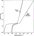
Fig. 4A shows simulated VGate and QGate plots for a disclosed LDMOS device (shown as a "10V new LDMOS") similar to LDMOS device 200 with LOCOS layer 137 and a known LDMOS device (shown as a "known LDMOS 7V ISO LDMOS"). As described above, known LDMOS devices have a DWELL early in the process (before the gate), which is believed to produce a misalignment between the DWELL diffusion and the edge of the polysilicon gate, which results in the L of the LDMOS deviceEFFAt least 200nm, usually ≥ 500nm (0.5 μm). Qgate is shown to be significantly improved by the short Leff (about 100nm) and LOCOS layers provided.
Fig. 4B shows simulated data for rds. qgtot of the disclosed LDMOS device (shown as "new LDMOS") and a known LDMOS device. Qgtot is shown to be greatly reduced by the disclosed LDMOS device. Fig. 4C shows simulated data for RSP of the disclosed LDMOS device (again shown as "new LDMOS") and a known LDMOS device. RSP is shown to be greatly reduced by the disclosed LDMOS device as well. These parameters are significantly improved over known LDMOS devices while also finding the ability to hold the LDMOS device against drain voltage (i.e., without sacrificing drain-source Breakdown Voltage (BVDSS)) and maintaining low junction leakage.
The disclosed embodiments can be used to form semiconductor chips that can be integrated into various assembly flows to form a variety of different devices and related products. The semiconductor chip may include various components therein and/or layers thereon, including barrier layers, dielectric layers, device structures, active components, and passive components, including source regions, drain regions, bit lines, bases, emitters, collectors, conductive lines, conductive vias, and the like. In addition, the semiconductor chip can be formed by various processes including bipolar, Insulated Gate Bipolar Transistor (IGBT), CMOS, BiCMOS, and MEMS.
Those skilled in the art to which the disclosure relates will appreciate that many other embodiments and variations of embodiments are possible within the scope of the claimed invention, and that further additions, deletions, substitutions and modifications may be made to the described embodiments without departing from the scope of the disclosure.