CN106664510B - Receivers for Backscatter Communications - Google Patents
Receivers for Backscatter Communications Download PDFInfo
- Publication number
- CN106664510B CN106664510B CN201580036187.3A CN201580036187A CN106664510B CN 106664510 B CN106664510 B CN 106664510B CN 201580036187 A CN201580036187 A CN 201580036187A CN 106664510 B CN106664510 B CN 106664510B
- Authority
- CN
- China
- Prior art keywords
- data
- backscatter
- subset
- high speed
- frequency
- Prior art date
- Legal status (The legal status is an assumption and is not a legal conclusion. Google has not performed a legal analysis and makes no representation as to the accuracy of the status listed.)
- Active
Links
Images


Classifications
-
- H—ELECTRICITY
- H04—ELECTRIC COMMUNICATION TECHNIQUE
- H04B—TRANSMISSION
- H04B5/00—Near-field transmission systems, e.g. inductive or capacitive transmission systems
- H04B5/70—Near-field transmission systems, e.g. inductive or capacitive transmission systems specially adapted for specific purposes
- H04B5/72—Near-field transmission systems, e.g. inductive or capacitive transmission systems specially adapted for specific purposes for local intradevice communication
-
- H—ELECTRICITY
- H04—ELECTRIC COMMUNICATION TECHNIQUE
- H04W—WIRELESS COMMUNICATION NETWORKS
- H04W4/00—Services specially adapted for wireless communication networks; Facilities therefor
- H04W4/80—Services using short range communication, e.g. near-field communication [NFC], radio-frequency identification [RFID] or low energy communication
-
- H—ELECTRICITY
- H04—ELECTRIC COMMUNICATION TECHNIQUE
- H04B—TRANSMISSION
- H04B5/00—Near-field transmission systems, e.g. inductive or capacitive transmission systems
- H04B5/70—Near-field transmission systems, e.g. inductive or capacitive transmission systems specially adapted for specific purposes
- H04B5/77—Near-field transmission systems, e.g. inductive or capacitive transmission systems specially adapted for specific purposes for interrogation
-
- H—ELECTRICITY
- H04—ELECTRIC COMMUNICATION TECHNIQUE
- H04B—TRANSMISSION
- H04B7/00—Radio transmission systems, i.e. using radiation field
- H04B7/22—Scatter propagation systems, e.g. ionospheric, tropospheric or meteor scatter
-
- H—ELECTRICITY
- H04—ELECTRIC COMMUNICATION TECHNIQUE
- H04L—TRANSMISSION OF DIGITAL INFORMATION, e.g. TELEGRAPHIC COMMUNICATION
- H04L27/00—Modulated-carrier systems
- H04L27/32—Carrier systems characterised by combinations of two or more of the types covered by groups H04L27/02, H04L27/10, H04L27/18 or H04L27/26
- H04L27/34—Amplitude- and phase-modulated carrier systems, e.g. quadrature-amplitude modulated carrier systems
- H04L27/345—Modifications of the signal space to allow the transmission of additional information
- H04L27/3455—Modifications of the signal space to allow the transmission of additional information in order to facilitate carrier recovery at the receiver end, e.g. by transmitting a pilot or by using additional signal points to allow the detection of rotations
-
- H—ELECTRICITY
- H04—ELECTRIC COMMUNICATION TECHNIQUE
- H04L—TRANSMISSION OF DIGITAL INFORMATION, e.g. TELEGRAPHIC COMMUNICATION
- H04L27/00—Modulated-carrier systems
- H04L27/32—Carrier systems characterised by combinations of two or more of the types covered by groups H04L27/02, H04L27/10, H04L27/18 or H04L27/26
- H04L27/34—Amplitude- and phase-modulated carrier systems, e.g. quadrature-amplitude modulated carrier systems
- H04L27/38—Demodulator circuits; Receiver circuits
-
- H—ELECTRICITY
- H04—ELECTRIC COMMUNICATION TECHNIQUE
- H04W—WIRELESS COMMUNICATION NETWORKS
- H04W88/00—Devices specially adapted for wireless communication networks, e.g. terminals, base stations or access point devices
- H04W88/08—Access point devices
Landscapes
- Engineering & Computer Science (AREA)
- Computer Networks & Wireless Communication (AREA)
- Signal Processing (AREA)
- Near-Field Transmission Systems (AREA)
Abstract
A backscatter receiving module and a method of backscatter communication are described. The front end module receives the backscatter signal from the antenna and generates high speed and low speed data. The high speed data decoding module outputs first data in response to high speed data having high speed symbols encoded at a first frequency. The high speed symbols include a first subset of symbols and a second subset of symbols. The low-speed decoding module outputs second data in response to the received low-speed data, which is encoded into the backscatter signal at a second frequency. The low-speed decoding module generates a first state of the second data when the high-speed symbols are in the first subset over a length of time. The low-speed module generates a second state of the second data when the high-speed symbols of the high-speed data are in the second subset for the length of time.
Description
Cross Reference to Related Applications
This application is related to U.S. patent application No.14/502,167, entitled "Device for backscatter Communication," attorney docket No. 7171P278, filed 9/30/2014, and is currently being processed.
Technical Field
This disclosure relates generally to backscatter communications and, in particular, but not exclusively, to radio frequency identification ("RFID") receivers.
Background
Radio frequency identification ("RFID") communications are one example of backscatter communications. RFID communications typically include a "base station transceiver" that broadcasts/transmits electromagnetic energy and then interprets data from reflections of the broadcasted electromagnetic energy. The "tag" reflects a portion of the electromagnetic energy back to the base station to communicate data to the reader. To encode data (e.g., an identification number) in the reflected portion, a passive (batteryless) tag may extract power from the broadcast electromagnetic energy and use the extracted power to modulate the electromagnetic energy reflected back to the base station. In contrast, battery powered tags use a battery to power circuitry that modulates the electromagnetic energy reflected back to the base station. Passive tags typically have a much shorter range than battery powered tags.
Backscatter communications, including RFID communication systems, are increasingly important because tags can be made relatively small and RFID communications do not require line-of-site (line-of-site) communication between a base station and the tag. As RFID communications become more prevalent, the need to transmit larger amounts of information in shorter periods of time using backscatter communications increases.
Drawings
Non-limiting and non-exclusive embodiments of the present invention are described with reference to the following figures, wherein like reference numerals refer to like parts throughout the various views unless otherwise specified.
Fig. 1 illustrates a backscatter communication system including a base station and a tag in accordance with an embodiment of the disclosure.
Fig. 2A is a functional block diagram illustrating a base station for assisting in backscatter communications according to an embodiment of the disclosure.
Fig. 2B is a functional block diagram illustrating an exemplary backscatter receiving circuit according to an embodiment of the disclosure.
Fig. 3A illustrates a block diagram of an apparatus including an exemplary tag in accordance with an embodiment of the present disclosure.
Fig. 3B illustrates a block diagram of an apparatus including an exemplary tag in accordance with an embodiment of the present disclosure.
Fig. 4A shows a graph showing a voltage signal over time according to an embodiment of the disclosure.
Fig. 4B illustrates an enlarged section of the graph in fig. 4A, according to an embodiment of the disclosure.
Fig. 5 shows a graph showing a vector radar cross section of an antenna according to an embodiment of the present disclosure over time.
Fig. 6 shows a flow diagram illustrating a tag-side method of backscatter communications according to an embodiment of the disclosure.
Fig. 7 shows a flow chart illustrating a method of backscatter communication with a base station in accordance with an embodiment of the disclosure.
Detailed Description
Embodiments of systems and methods for backscatter communications are described herein. In the following description, numerous specific details are set forth in order to provide a thorough understanding of the embodiments. One skilled in the relevant art will recognize, however, that the techniques described herein can be practiced without one or more of the specific details, or with other methods, components, materials, and so forth. In other instances, well-known structures, materials, or operations are not shown or described in detail to avoid obscuring aspects.
Reference throughout this specification to "one embodiment" or "an embodiment" means that a particular feature, structure, or characteristic described in connection with the embodiment is included in at least one embodiment of the present invention. Thus, appearances of the phrases "in one embodiment" or "in an embodiment" in various places throughout this specification are not necessarily all referring to the same embodiment. Furthermore, the particular features, structures, or characteristics may be combined in any suitable manner in one or more embodiments.
Fig. 1 shows a backscatter communication system 100 according to an embodiment of the disclosure, the backscatter communication system 100 comprising a base station transceiver 103 and a tag included in a mobile device 101. Backscatter communication system 100 provides wireless communication links of short range (e.g., up to 20m), high bandwidth (e.g., 20 to 100Mbps), and low power (e.g., less than 1mW) using backscatter communication to deliver data from one or more mobile devices 101 to base station 103. One example of backscatter communications is commonly referred to as radio frequency identification ("RFID"). RFID is often used to wirelessly communicate an identification code of a target (e.g., electronic card, consumer product). However, backscatter communication including RFID can also be used to stream (stream) data sets larger than just the identification code/number.
The backscatter communication link is implemented by integrating a backscatter tag (e.g., a semi-passive tag) into the mobile device 101. This design takes advantage of the asymmetric power budget between the wired base station 103 and the mobile device 101 to provide a low power solution on the mobile device side by relying on the power available at the base station side at all times.
Some radio frequency identification ("RFID") tags are completely passive devices that do not include a separate power source and draw energy from the EM energy 104 to operate. However, extracting energy from EM energy 104 effectively slows the data rate of the backscatter channel, as the backscatter antenna will typically be optimized for extracting power without having to increase the signal-to-noise ratio ("SNR") of the backscatter channel. Furthermore, fully passive RFID tags often pause for periodic power acquisition, which interrupts or delays data transmission. The energy harvesting reduces the read range of the base station 103 because more incident EM radiation 104 is required to power the backscatter tag than is required for backscatter communication alone. Conventional fully passive backscatter tags employ slower data rates because the power consumption on the backscatter tag is highly dependent on the clock speed.
Embodiments of backscatter tags embedded within mobile device 101 may be part of a passive device that does not require energy extraction from EM radiation 104. However, the backward radiating tags are powered by the main battery of the mobile device 101. Because modulating the impedance load requires a modest power budget (e.g., 15 μ W), backscatter transmission does not significantly affect battery life. Furthermore, by not drawing power from EM energy 104, the backscatter antenna and modulation load impedance can be optimized for reflected EM energy 104 to improve SNR, reduce bit rate errors, and improve data throughput of the backscatter channel. By not drawing power from EM energy 104 to power backscatter tags, some embodiments disclosed herein may operate at higher clock rates and greater data throughput. Other embodiments of the present disclosure may harvest energy from the EM energy 104.
Mobile device 101 represents a variety of different apparatuses, including a mobile phone 101A, a head mounted display 101B, a smart wristwatch 101C, a tablet, a laptop, a body-mountable apparatus, a body-implantable article, or other mobile device operating with a limited power budget. Embodiments disclosed herein provide a backscatter channel having sufficient bandwidth to wirelessly stream data (e.g., video data, audio data, text data) from mobile device 101 to base station 103. The base station 103 may then transmit the streamed data to other devices, such as a television, server, or other mobile device, via a wired connection (e.g., ethernet) or a wireless connection (e.g., WiFi). In the illustrated embodiment, the base station 103 is a stand-alone box. In other embodiments, the base station 103 is integrated into a television, home computer, computer monitor, WiFi access point, cable modem, hard drive, router, set-top box, or other electronic device. In embodiments where the base station 103 is or is included in a WiFi access point, the EM energy 104 may be a WiFi transmission and the tag may reflect the EM energy 104 back to the base station 103.
Fig. 2A is a functional block diagram illustrating a base station 203 for assisting in backscatter communications according to an embodiment of the disclosure. Base station 203 is one possible implementation of base station 103 shown in fig. 1. The illustrated embodiment of base station 203 includes a backscatter transceiver 205, backscatter antennas 210 and 215, control circuitry 220, wired interface(s) 230, a power regulator 235, and one or more wireless communication antennas 242. The illustrated embodiment of backscatter transceiver 205 includes backscatter transmit circuitry 245 and backscatter receive circuitry 250. The illustrated embodiment of control circuit 220 includes logic 287. Fig. 2A shows the functional components of the base station 203, not necessarily the structural layout. It should be understood that the components of the base station 203 may be implemented entirely in hardware, entirely in software/firmware, or using a mixture of both software/firmware and hardware.
Wireless interface(s) 240 represent one or more wireless communication channels that do not use backscatter communication. For example, the wireless interface(s) 240 may be implemented using a WiFi transceiver, a bluetooth transceiver, an infrared transceiver, or other standardized/proprietary wireless communication systems. Wireless interface(s) 240 may facilitate non-backscatter communications with mobile device 101 or other devices. The wireless interface(s) 240 may also provide wireless network connectivity for the base station 203 to the internet or other consumer products (e.g., network attached storage, etc.).
The wired interface(s) 230 include any number of wired communication ports. For example, the wired interface 230 may include an ethernet controller, a universal serial bus ("USB") port, and the like. The ethernet controller may also provide a network connection.
The power regulator 235 provides a wired power connection for powering the internal components of the base station 203. Since base station 203 is a wired device, it is not constrained by a limited power budget as mobile device 101. Backscatter communications take advantage of this asymmetric power budget by pushing the power requirements to generate EM energy 212 into base station 203, while mobile device 101 operates by reflecting EM energy 212 generated at base station 203 (rather than independently generating EM radiation).
The control circuit 220 is the operating brain of the base station 203. It includes logic 287 for coordinating the operation of other functional components, and includes a field programmable gate array ("FPGA") and/or a processor for performing computations. Logic 287 may comprise hardware logic or software/firmware instructions stored on one or more storage devices. For example, logic 287 may include instructions for establishing a wireless session with one or more mobile devices 101, configuring and managing a wireless display session, and terminating a wireless display session.
Many commercial backscatter tags operate by encoding data with two discrete states. However, by using a larger number of states (increasing the available communication symbol constellation), quadrature amplitude modulation ("QAM") can be implemented to deliver higher data rates in backscatter communications. For example, using 16 states (e.g., 16-QAM) may result in a quadruple data rate at a lower SNR tradeoff. Furthermore, pairing increased communication symbols with increased data frequencies has been shown to enable very high data rates (e.g., -100 Mbps). Higher data rates may be used to stream data (e.g., cloud backup, video data) for large data applications.
To increase the clustering of available communication symbols beyond two data states (e.g., the numbers zero and one), the tags involved in backscatter communications must be able to produce an increased number of communication symbols. Furthermore, generating an increased number of communication symbols at higher frequencies allows for high speed channels with higher data rates than conventionally available. However, to ensure that the tags are also able to communicate using a conventional low speed scheme (having two data states), tags that can communicate data using both the low speed scheme and the disclosed high speed data transmission are advantageous. Accordingly, the tags disclosed in the present disclosure are configured to enable high speed data transmission and are backward compatible with conventional (e.g., "Gen 2") low speed RFID protocols to ensure that the data tags are able to communicate with existing base stations that utilize existing RFID protocols. Conventional low speed data may be transmitted at 125kHz while higher speed data may be transmitted at 25 MHz.
Fig. 3A illustrates a block diagram of an apparatus 310A including an example tag 307A, according to an embodiment of the disclosure. The apparatus 310A may be one of the mobile devices depicted in fig. 1. The example device 310A includes a battery 326, a processor 350, a sensor 375, a first analog-to-digital converter ("ADC") 361, a second ADC 363, and an antenna 345. Tag 307A includes modulation circuitry 330 and encoding module 320.
Modulation circuit 330 is coupled to apply a plurality of impedance values (Z in fig. 3A) to the antenna0-Z31) Modulates the antenna 345. Changing the impedance value of the antenna 345 is one way to change the vector radar cross-section of the device 310A. Changing the vector radar cross section may change the backscatter signal 217 reflected by antenna 345 back to base station 203, which allows tag 307A to transmit data back to base station 203.
The modulation circuit 330 includes an A 'modulation circuit 331, a B' modulation circuit 332, and a 2-1 multiplexer ("MUX") 339. The A' modulation circuit may be only in the first subset Z of impedance values0-Z15Modulates the impedance of the antenna 345. Impedance Z0-Z15Which functions to communicate sixteen symbols (e.g., implementing 16-QAM signaling) that may be used for communication with base station 203. The B' modulation circuit may be only at a second subset Z of impedance values16-Z31Modulates the impedance of the antenna 345. Impedance Z16-Z31Acting as sixteen corresponding symbols (symbols), e.g. impedance Z0-Z15That communicates the same symbols. For example, in one embodiment, antenna 345 is adjusted to impedance Z0Will be like adjusting the antenna 345 to impedance Z16That communicates the same symbol to the base station 203. In this example, Z0And Z16Are the corresponding impedances communicating the same corresponding symbol. It should be understood that there are 32 impedance values (Z) comprising a subset of 16 impedance values0-Z31) Are exemplary only, and differ inMore or fewer impedance values may be utilized in embodiments of the invention.
Encoding module 320 includes a 'selector logic 325 and B' selector logic 327. The encoding module 320 may be configured to modulate the modulation module 330 at a plurality of impedances Z0-Z31To encode the first data 391 at a first higher frequency (CLK 1). The encoding module 320 is also coupled to direct the modulation module 330 at a plurality of impedances Z0-Z31First subset Z of0-Z15Or a second subset Z16-Z31To encode the second data 392 at a second frequency (CLK 2). CLK2 operates at a frequency lower than CLK 1.
In fig. 3A, a' selector logic 325 is coupled to receive first data 391 and CLK1 operating at a first frequency. The A 'selector logic 325 is coupled to modulate the signal at Z by directing the A' modulation circuit 331 at Z0-Z15To encode the first data 391 at the first frequency. B' selector logic 327 is also coupled to receive first data 391 and CLK 1. B 'selector logic 327 is coupled to operate by directing B' demodulation circuit 332 at Z16-Z31To encode the first data 391 at the first frequency. MUX 339 is coupled to receive data 392. The digital value of the second data 392 changes corresponding to CLK2, which CLK2 has a lower frequency than the first data 391 and CLK 1. The digital values of data 392 cause 2-1 MUX 339 to couple either the impedance values from a 'modulation circuit 331 or the impedance values from B' modulation circuit to antenna 345. Thus, when second data 392 has a first state (e.g., a digital zero), the impedance values applied to antenna 345 are limited to a first subset of impedance values for a' modulation circuitry 331; and, when second data 392 has a second state (e.g., a digital one), the impedance values applied to antenna 345 are limited to a second subset of the impedance values of B' modulation circuitry 332.
The A 'selector logic 325 and B' selector logic 327 may be implemented using microcontrollers, logic arrays, discrete logic, or custom application specific integrated circuits ("ASICs"). The A' modulation circuit 331 can use a transistor T0-T15Implementation of the transistor T0-T15Can be activated to connect different impedance values Z0-Z15To MUX 339 (and ultimately to antenna 345). Similarly, the B' modulation circuit 332 may use a transistor T16-T31Implementation of the transistor T16-T31Can be activated to connect different impedance values Z16-Z31. Of course, other non-transistor switchers capable of switching at high frequencies may be used in place of transistors. Those skilled in the art will also appreciate that alternative techniques and configurations for connecting different impedance values to antenna 345 may be implemented.
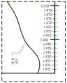
Attention is directed to fig. 5 to further illustrate how fig. 3A communicates both high-speed and low-speed data streams via a backscatter technique. Fig. 5 is a diagram showing a change in vector radar cross section of an antenna in a tag over time according to an embodiment of the present disclosure. It should be understood that the vector RCS values in fig. 5 are shown to convey the general concept of providing different vector RCS values to the antennas, but in operation, the vector RCS would comprise complex vector RCS rather than strictly real vector RCS values. Further, the impedance value applied to the antenna to provide a given vector RCS value for the antenna may be a complex impedance value. Fig. 5 shows a first, second, third and fourth cycle. Each period corresponds to a period associated with the frequency of CLK 2. The collection of vectors RCS at the first, second, third and fourth cycles are shown as groups 401, 402, 403 and 404, respectively.
During a first period, antenna 345 is modulated to different vector RCS values (e.g., by applying different impedance values to antenna 345) to encode first data 391 as different symbols with a first subset of impedance values (e.g., Z)0-Z15) And (7) corresponding. During the second period, antenna 345 is also modulated to different vector RCS values to encode first data 391 as different symbols corresponding to the second subset of impedance values. A first set 401 of vector RCS values is near the center radar value 421 and a second set 402 of vector RCS values is closer to the center radar value 422. The first data state (e.g., digital zero) of the second data 392 is communicated when the vector RCS value of antenna 345 is closer to the center radar value 421 in a period of a CLK2, and the second data 3 is communicated when the vector RCS value is closer to the center radar value 422 in a period of a CLK292 (e.g., a digital one). Thus, groups 401, 402, 403, and 404 in the first, second, third, and fourth periods in FIG. 5 convey that the second data 392 is "0-1-0-0". By modulating antenna 345 in this manner, tag 307A may communicate first data 391 as high-speed data corresponding to CLK 1; and encodes the second data by switching between the first subset of impedance values and the second subset of impedance values to communicate the second data 392 as low speed data corresponding to CLK 2. Since the tag must switch between subsets of impedance values to communicate low speed data, each symbol in the cluster of symbols being communicated has an impedance value in a first subset to communicate that symbol and a corresponding impedance value in a second subset to also communicate that symbol, a particular high speed symbol can be communicated regardless of whether the first or second subset of impedance values is being used. Of course, changing the impedance value (to change the vector RCS of the antenna) is merely an embodiment of modulating the backscatter signal by adjusting the in-phase and out-of-phase (i.e., I and Q quadrature) properties of the backscatter signal that is reflected back to the base station.
The base station receiving the backscattered signal from tag 307A may apply a filter having a cutoff frequency between the first frequency (CLK1) and the second frequency (CLK2) to isolate the second data 392. Applying the filter will filter out the higher frequency data, but the combination of the higher frequency symbols will still pass, wherein radar signals closer to corresponding to the center radar value 421 or the center radar value 422 indicate two different discrete states of the lower speed second data 392. It should be understood that the word "center" in the term "center radar value" may be associated with a particular mapping, such as a particular region of a Smith Chart (Smith Chart), which is a mapping from a backscattered signal to a signal received by a base station. Such mapping does not have to be linearly related to the impedance of the tag, is not necessarily evenly distributed, depends largely on the RF link between the tag and the base station, and is highly dependent on the clustering of the vector RCS values employed.
Returning to fig. 3A, sensor 375 is coupled to provide signal 371 to both ADC 1361 and ADC 2362. Signal 371 may be a voltage, a current, or the like. The sensor 375 may be a biosensor that measures, for example, glucose or heart rate. ADC 1361 samples signal 371 at a first frequency associated with CLK 1. ADC 1362 samples signal 371 at a second frequency associated with CLK 2.
Fig. 4A and 4B show that the first frequency (CLK1) is a higher frequency than the second frequency (CLK 2). The diagram of fig. 4A shows the voltage of signal 471 as a function of time, and the diagram of fig. 4B shows an enlarged portion of the diagram in fig. 4A, according to an embodiment of the disclosure.
The signal 471 is an example of the signal 371. Since ADC 1361 samples signal 471 at a faster rate than ADC 2362 samples signal 471, first data 391 has a higher resolution than second data 392. In one example, only one ADC is used to sample the signal at the first frequency (CLK1) and a subset of the signal sampled at the second frequency (CLK2) is transmitted as the second data 392. For example, the ADC may choose to correspond to the second data 392 every tenth or every hundred samples. Alternatively, data from one ADC may be processed to provide summarized data (summary data) as second data 392. One application of this embodiment is to transmit electrocardiogram ("ECG") cardiac signals, where the waveform signal has diagnostic details on a higher frequency, but a lower frequency may still indicate beats per minute. When tag 307A encodes both first data 391 and second data 392 by changing the impedance of antenna 345, it may encode both higher resolution first data 391 and lower resolution second data 392. Thus, a base station configured to read a higher speed data protocol will be able to receive the higher resolution first data 391. However, if the base station is not configured to read the higher speed data protocol (legacy base station), it will be able to read the lower speed data protocol and will still be able to receive the lower speed second data 392. The lower speed data 392 protocol will be EPC Gen2 backward compatible so that legacy base stations can read the lower speed data 392.
Fig. 3B illustrates a block diagram of an apparatus 310B including an example tag 307B, according to an embodiment of the disclosure. Tag 307B shows a different hardware configuration that performs the same functions described with respect to tag 307A. Tag 307B includes an encoding module 340 and a modulation circuit 351. Modulation circuit 351 is coupled to operate at a plurality of impedance values Z0-ZNModulates the antenna 345. The encoding module 340 is coupled to modulate the modulation module 351 at its impedance value Z0-ZNTo encode the first data at the first frequency. The encoding module 340 is also coupled to modulate the modulation module 351 at a plurality of impedances Z0-ZNIs selected to encode second data at a second frequency. The encoding module 340 includes selector logic 343. Selector logic 343 may be implemented with a microprocessor or discrete logic. Selector logic 343 receives first data 391 and second data 392. When the second data 392 is the first data state (e.g., digital zero), the selector logic 343 limits its impedance value Z0-ZNA first subset of the impedance values is selected. When the second data 392 is a second data state (e.g., a digital one), the selector logic 343 limits its impedance value Z0-ZNTo a second subset of the impedance values.
The device 310B includes a sensor 377, a sensor 379, a first ADC 361, and a second ADC 363. Sensor 377 provides signal 372 to first ADC 361 and sensor 379 provides signal 373 to second ADC 363. Sensor 379 may be a heart rate sensor and sensor 377 may sense audio data (e.g., a microphone). In one embodiment, sensors requiring a lower data rate are coupled to generate second data 392, while sensors requiring a higher data rate are coupled to generate first data 391. It should be understood that different sensor configurations shown in fig. 3A and 3B may be used in either figure to generate first data 391 and second data 392.
In the example shown in fig. 3A and 3B, the first subset of impedance values may include impedance values that are common to the second subset of impedance values. In various embodiments, the first subset of impedance values may not share impedance values with the second subset of impedance values.
After tag 307A or 307B encodes data into backscatter signal 217, backscatter signal 217 is received by antenna 215 and decoded by backscatter receiving circuitry 250. Fig. 2B shows a functional block diagram of an exemplary backscatter receiving module 251, the backscatter receiving module 251 being one possible example of a backscatter receiving circuit 250, in accordance with an embodiment of the disclosure.
Mixing block 252 is coupled to receive backscatter signal 217 from receive antenna 215 and is coupled to receive a carrier frequency 253. The carrier frequency 253 will be the same as the frequency of the EM energy 212 (transmission signal) and the mixing block 252 multiplies the backscatter signal 217 by the carrier frequency 253 to isolate (isolate) the modulated portion of the backscatter signal 217 containing the data. The modulated portion of the backscatter signal continues to the front end module 255. Both high speed filter 257 and low speed filter 256 receive the backscatter signals because they are configured in parallel in fig. 2B. The backscattered signal may optionally be amplified before reaching the filter.
The low-speed filter 256 is configured to isolate low-speed data from high-speed data. If high speed data is encoded into the backscatter signal 217 by a tag (e.g., 307A or 307B) at a first frequency (e.g., 25MHz) and low speed data is encoded at a second frequency (e.g., 125kHz), the low speed filter 256 isolates the low speed data by filtering out frequencies above 125 kHz. For example, the low-speed filter 256 may be a low-pass filter having a cutoff frequency between the first frequency and the second frequency. Thus, the low speed filter 256 passes low speed data in response to the backscatter signal. Because the low-speed filter 256 filters out high-speed transitions of the high-speed data, the values of the high-speed symbols are effectively averaged. The filtering determines whether the high speed signal in a given time period is from a first subset of symbols or a second subset of symbols, as the value of the low speed data will indicate which subset of symbols was used during the given time period. When a high speed symbol is being received in the first subset (for a particular length of time), it indicates a first state of low speed data (e.g., zero), and when a high speed symbol is being received in the second subset (for a particular length of time), it indicates a second state of low speed data (e.g., one). The length of time that the high speed symbol needs to remain in a subset to indicate a particular data state corresponds to the period of the second frequency (e.g., 125 kHz).
The high speed symbols include a first subset of symbols and a second subset of symbols. The first subset of symbols may correspond to the first subset of impedance values depicted in fig. 3A and 3B. Similarly, the second subset of symbols may correspond to the second subset of impedance values depicted in fig. 3A and 3B. Each symbol in the first subset has a corresponding symbol in the second subset, such that whether the tag uses the first subset of vector radar cross-sections of the antenna (which result from the first subset of impedances) or the second subset of vector radar cross-sections of the antenna (which result from the second subset of impedances),the tags can communicate complete clusters of symbols. Even if different symbols are used, the corresponding symbols communicate the same data value. In one embodiment, Z0And Z16Corresponds to, Z1And Z17Correspond to15And Z31And (7) corresponding. So in this embodiment, antenna 345Z is given0Or Z16The same symbol or data feature (character) is communicated.
High-speed decoding module 281 receives high-speed data 258 and low-speed decoding module 283 receives low-speed data 259. High speed decoding module 281 is configured to generate first data 271 by decoding high speed symbols encoded at a first frequency (e.g., 25 MHz). The tag may encode the high-speed symbol at a first frequency (CLK1) by modulating the impedance of antenna 345. If the tag is using QAM, high speed decoding module 281 will include a QAM decoding unit. Low-speed decoding module 283 is configured to output second data 272 in response to low-speed data 259, which is encoded at a second frequency (e.g., 125 kHz). The tag may encode the low speed data at the second frequency (CLK2) by driving MUX 339 to limit the impedance value of antenna 345 to the first subset or the second subset of impedance values corresponding to circuits 331 or 332.
In FIG. 2B, the high speed decoding module 281 comprises a 2-1 symbol translation unit 282. Since the high speed symbols include a first subset and a second subset of symbols, and a given symbol in the first subset has a corresponding symbol in the second subset that communicates the same symbol or data characteristic, the symbol translation unit 282 outputs the appropriate data characteristic in response to receiving either of the corresponding symbols. The decoding module 280 may also include a checksum (checksum) to ensure accurate data reception.
Fig. 6 shows a flow chart illustrating a process of tag side backscatter communication according to an embodiment of the disclosure. The order in which some or all of the process blocks appear in process 600 should not be considered limiting. Rather, persons of ordinary skill in the art having benefit of the present disclosure will appreciate that certain processing blocks may be performed in a variety of orders, even in parallel, not shown.
In a process block 605, electromagnetic energy (e.g., EM energy 212) is received from a base station. In process block 610, first data is encoded (at a first frequency) by adjusting a radar cross-section of a device between a plurality of radar cross-sections. In the example shown in fig. 3A and 3B, the vector radar cross-section of antenna 345 is adjusted by modulating the impedance of the antenna between a plurality of impedance values. However, there are other ways of adjusting the radar cross section of the device. For example, a microelectromechanical system ("MEMS") can be manipulated to change the radar cross-section of the device. For example, MEMS that adjust the tilt of a radar reflecting material (e.g., metal) also changes the radar cross section of the device. Furthermore, multiple MEMS can be manipulated in multiple modes (in addition to tilt control) to produce different radar cross sections. Other ways of adjusting the radar cross section of the device include immersing (infuse) a metallic substance into a liquid crystal and using the liquid crystal to control the alignment of the metallic substance and thereby change the radar cross section of the device. Here, in addition, an array of independently selectable liquid crystals with immersed metallic substances will also produce additional adjustability of the radar cross section to produce a plurality of different radar cross sections. Other methods of adjusting the radar cross section include varactor diodes, PIN diodes, variable attenuators, and variable phase shifters.
In process block 615, second data is encoded (at a second frequency lower than the first frequency) by limiting adjustment of the plurality of radar cross sections over a period of time. The time period corresponds to a period of the second frequency. The process 600 continues with encoding the first data and the second data to communicate the desired amount of data to the base station as needed.
Fig. 7 shows a flow chart illustrating a method of backscatter communication with a base station in accordance with an embodiment of the disclosure. The order in which some or all of the process blocks appear in process 700 should not be considered limiting. Rather, persons of ordinary skill in the art having benefit of the present disclosure will appreciate that certain processing blocks may be performed in a variety of orders, even in parallel, not shown.
In process block 705, a backscatter signal (e.g., backscatter signal 217) is received with a backscatter receive antenna (e.g., antenna 215). The backscatter signal is a modulated version of an electromagnetic transmission signal transmitted by a transmission antenna (e.g., antenna 210). In some embodiments, the backscatter receiving antenna and the transmission antenna may be the same antenna. The transmitted signal may be reflected back by a tag within the mobile device (e.g., apparatus 310) as a modulated backscatter signal.
In step 710, the high speed symbols encoded into the backscatter signal are decoded. The high speed symbols are encoded into the backscatter signal at a first frequency (e.g., 25 MHz).
In process block 715, the high speed symbol is translated into first data (e.g., data 271). The high speed symbols include a first subset of symbols and a second subset of symbols. Corresponding symbols from the first subset and the second subset are translated to have the same data characteristics in the first data.
In a process block 720, second data (e.g., data 272) is decoded in response to the low speed data encoded into the backscatter signal. Low-speed data is encoded into the backscatter signal at a second frequency (e.g., 125kHz) that is less than the first frequency at which the high-speed symbols are encoded. Since tag 307A encodes the second data by transmitting a first subset of high speed symbols over a length of time (e.g., between signals of CLK2) to indicate a first state (e.g., a digital zero) of the second data, and by transmitting a second subset of high speed symbols to indicate a second state (e.g., a digital one) of the second data, the second data obtains the first state when the high speed symbols last in the first subset for a specified length of time, and the second data obtains the second state when the high speed symbols last in the second subset for that length of time. In one embodiment, the length of time corresponds to a period of the second frequency.
It should be understood that processing blocks 710, 715, and 720 may be performed in parallel, or they may be performed in series. Process 700 may repeat to continue decoding data from the backscattered signal. It should be understood that a base station utilizing process 700 will be able to decode high speed data as well as support low speed data. Thus, tags that transmit only low speed data will be compatible with the base station, and tags that transmit only high speed data (e.g., using QAM) will also be compatible with the base station. Further, tags that can transmit both low-speed data and high-speed data will also be compatible with a base station (e.g., base station 203) using process 700.
The process explained above is described in terms of computer software and hardware. The techniques may constitute machine-readable instructions embedded within a tangible or non-transitory machine (e.g., computer) readable storage medium, which when executed by a machine, will cause the machine to perform the operations described. Further, the processes may be implemented within hardware, such as an application specific integrated circuit ("ASIC").
A tangible, non-transitory, machine-readable storage medium includes any mechanism that provides (i.e., stores) information in a form accessible by a machine (e.g., a computer, network device, personal digital assistant, manufacturing tool, any device with a set of one or more processors, etc.). For example, a machine-readable storage medium includes recordable/non-recordable media (e.g., Read Only Memory (ROM), Random Access Memory (RAM), magnetic disk storage media, optical storage media, flash memory devices, etc.).
The embodiments of the invention described above, including those described in the abstract, are not intended to be exhaustive or to limit the invention to the precise forms disclosed. While specific embodiments of, and examples for, the invention are described herein for illustrative purposes, various modifications are possible within the scope of the invention, as those skilled in the relevant art will recognize.
These variations can be made to the invention in light of the above detailed description. The terms used in the following claims should not be construed to limit the invention to the specific embodiments disclosed in the specification. The scope of the invention is to be determined entirely by the following claims, which are to be construed in accordance with established doctrines of claim interpretation.
Claims (22)
1. A base station, comprising:
a receive antenna coupled to receive backscatter signals from backscatter tags;
a backscatter receiving module coupled to receive the backscatter signal, wherein the backscatter receiving module comprises:
a high speed decoding module configured to generate first data by decoding high speed symbols encoded into a backscatter signal at a first frequency, wherein the high speed symbols include a first subset having a plurality of first symbols and a second subset having a plurality of second symbols; and
a low speed decoding module configured to output second data in response to low speed data encoded into the backscatter signal at a second frequency, wherein the low speed decoding module is configured to produce a first state of the second data when the high speed symbols are in a first subset over a length of time, and wherein the low speed decoding module is configured to produce a second state of the second data when the high speed symbols of the high speed data are in a second subset over the length of time, the second frequency being lower than the first frequency.
2. The base station of claim 1, wherein each symbol in the first subset has a corresponding symbol in the second subset, and wherein the high speed decoding module comprises a symbol translation unit configured to output the same data characteristic of the first data when a given symbol from the first subset or its corresponding symbol from the second subset is received by the symbol translation unit.
3. The base station of claim 1, wherein the high speed decoding module comprises a quadrature amplitude modulation ("QAM") decoding unit.
4. The base station of claim 1, wherein the length of time corresponds to a period of the second frequency.
5. The base station of claim 1, further comprising:
a transmitting antenna; and
a backscatter transmit circuit coupled to the transmit antenna to transmit the transmission signal as electromagnetic energy, wherein the backscatter signal received from the backscatter tag is a modulated version of the transmission signal.
6. The base station of claim 5, wherein the transmit antenna and the receive antenna are a common antenna.
7. The base station of claim 1, further comprising a mixing block coupled between the receive antenna and the high speed decoding module to mix the backscatter signal with a carrier frequency of the transmission signal, wherein the backscatter signal is a modulated version of the transmission signal.
8. The base station of claim 1, further comprising:
a high-speed filter; and
a low-speed filter in parallel with a high-speed filter, wherein the high-speed filter is coupled between a receive antenna and a high-speed decoding module, and wherein the low-speed filter is coupled between the receive antenna and the low-speed decoding module, the low-speed filter being a low-pass filter having a cutoff frequency between a first frequency and a second frequency.
9. A backscatter receiving module comprising:
a front end module coupled to generate high speed data and low speed data of a backscatter signal in response to receiving the backscatter signal, wherein the front end module is coupled to receive the backscatter signal from an antenna;
a high speed decoding module coupled to output first data in response to receiving the high speed data, wherein the high speed decoding module is configured to generate the first data by decoding high speed symbols encoded into a backscatter signal at a first frequency, and wherein the high speed symbols include a first subset having a plurality of first symbols and a second subset having a plurality of second symbols; and
a low speed decoding module coupled to output second data in response to receiving the low speed data, the low speed data encoded into the backscatter signal at a second frequency, wherein the low speed decoding module is configured to produce a first state of the second data when the high speed symbols of the high speed data are in a first subset for a length of time, and wherein the low speed decoding module is configured to produce a second state of the second data when the high speed symbols of the high speed data are in a second subset for the length of time, the second frequency being lower than the first frequency.
10. The backscatter receiving module of claim 9, wherein each symbol in the first subset has a corresponding symbol in the second subset, and wherein the high speed decoding module comprises a symbol translation unit configured to output the same first data characteristic of the first data when a given symbol from the first subset or its corresponding symbol from the second subset is received by the symbol translation unit.
11. The backscatter receiving module of claim 9, wherein the high speed decoding module comprises a quadrature amplitude modulation ("QAM") decoding unit.
12. The backscatter receiving module of claim 9, wherein the length of time corresponds to a period of the second frequency.
13. The backscatter receiving module of claim 9, further comprising:
a high-speed filter; and
a low speed filter in parallel with the high speed filter, wherein the high speed filter is coupled to pass high speed data in response to the backscatter signal, and wherein the low speed filter is coupled to pass low speed data in response to the backscatter signal, the low speed filter being a low pass filter having a cutoff frequency between a first frequency and a second frequency.
14. The backscatter receiving module of claim 13, wherein the high speed filter and the low speed filter are implemented by a processor configured as a software defined radio.
15. A method of backscatter communication, the method comprising:
receiving a backscatter signal with a backscatter receiving antenna;
decoding a high speed symbol encoded into the backscatter signal, wherein the high speed symbol is encoded into the backscatter signal at a first frequency;
translating high speed symbols into first data, wherein the high speed symbols comprise a first subset having a plurality of first symbols and a second subset having a plurality of second symbols; and
decoding second data in response to low speed data encoded into the backscatter signal at a second frequency, the second frequency being lower than the first frequency, wherein the low speed data has a first state when the high speed symbol is in a first subset for a length of time, and wherein the low speed data has a second state when the high speed symbol is in a second subset for the length of time.
16. The method of claim 15, wherein each symbol in the first subset has a corresponding symbol in the second subset, and wherein said translating the high speed symbols comprises outputting the same data characteristic of the first data in response to receiving a given symbol from the first subset or its corresponding symbol from the second subset.
17. The method of claim 15, further comprising:
transmitting an electromagnetic transmission signal via a transmit antenna, wherein the backscatter signal is a modulated version of the electromagnetic transmission signal.
18. The method of claim 17, wherein the electromagnetic transmission signal is modulated by a tag within a mobile device.
19. The method of claim 15, further comprising:
a filter is applied to the backscatter signal to isolate the low speed data, wherein the filter has a cutoff frequency between the first frequency and the second frequency.
20. The method of claim 15, wherein the first subset and the second subset do not have overlapping symbols.
21. The method of claim 15, wherein the backscatter signal is a modulated version of a WiFi transmission signal from a base station that includes a receive antenna.
22. The method of claim 15, wherein the second data is compatible with Gen2 RFID protocols.
Applications Claiming Priority (3)
| Application Number | Priority Date | Filing Date | Title |
|---|---|---|---|
| US14/502,175 | 2014-09-30 | ||
| US14/502,175 US9357341B2 (en) | 2014-09-30 | 2014-09-30 | Receiver for backscatter communication |
| PCT/US2015/046595 WO2016053504A1 (en) | 2014-09-30 | 2015-08-24 | Receiver for backscatter communication |
Publications (2)
| Publication Number | Publication Date |
|---|---|
| CN106664510A CN106664510A (en) | 2017-05-10 |
| CN106664510B true CN106664510B (en) | 2020-05-19 |
Family
ID=55585934
Family Applications (1)
| Application Number | Title | Priority Date | Filing Date |
|---|---|---|---|
| CN201580036187.3A Active CN106664510B (en) | 2014-09-30 | 2015-08-24 | Receivers for Backscatter Communications |
Country Status (5)
| Country | Link |
|---|---|
| US (1) | US9357341B2 (en) |
| EP (1) | EP3201839B1 (en) |
| KR (1) | KR101907289B1 (en) |
| CN (1) | CN106664510B (en) |
| WO (1) | WO2016053504A1 (en) |
Families Citing this family (42)
| Publication number | Priority date | Publication date | Assignee | Title |
|---|---|---|---|---|
| US9680520B2 (en) | 2013-03-22 | 2017-06-13 | University Of Washington Through Its Center For Commercialization | Ambient backscatter tranceivers, apparatuses, systems, and methods for communicating using backscatter of ambient RF signals |
| US11163050B2 (en) | 2013-08-09 | 2021-11-02 | The Board Of Trustees Of The Leland Stanford Junior University | Backscatter estimation using progressive self interference cancellation |
| WO2015123306A1 (en) | 2014-02-11 | 2015-08-20 | University Of Washington | Apparatuses, systems, and methods for communicating using mimo and spread spectrum coding in backscatter of ambient signals |
| WO2015123341A1 (en) | 2014-02-11 | 2015-08-20 | University Of Washington | Wireless networking communication methods, systems, and devices operable using harvested power |
| WO2015168700A1 (en) | 2014-05-02 | 2015-11-05 | The Board Of Trustees Of The Leland Stanford Junior University | Method and apparatus for tracing motion using radio frequency signals |
| US10079616B2 (en) | 2014-12-19 | 2018-09-18 | University Of Washington | Devices and methods for backscatter communication using one or more wireless communication protocols including bluetooth low energy examples |
| US9668217B1 (en) * | 2015-05-14 | 2017-05-30 | Snap Inc. | Systems and methods for wearable initiated handshaking |
| EP3335432B1 (en) | 2015-08-12 | 2024-02-14 | University of Washington | Backscatter devices and network systems incorporating backscatter devices |
| CN108496094B (en) | 2016-01-26 | 2023-04-28 | 华盛顿大学 | A backscatter setup containing an example of SSB operation |
| US10652073B2 (en) | 2016-04-04 | 2020-05-12 | University Of Washington | Backscatter devices and systems providing backscattered signals including OFDM packets |
| GB201612175D0 (en) * | 2016-07-13 | 2016-08-24 | Univ Oslo Hf | Medical implant with wireless communication |
| DE102016216071B4 (en) * | 2016-08-26 | 2021-09-23 | Fraunhofer-Gesellschaft zur Förderung der angewandten Forschung e.V. | Concept for increasing performance in backscatter or load systems |
| US10812130B2 (en) | 2016-10-18 | 2020-10-20 | University Of Washington | Backscatter systems, devices, and techniques utilizing CSS modulation and/or higher order harmonic cancellation |
| EP3532981A4 (en) * | 2016-10-25 | 2020-06-24 | The Board of Trustees of the Leland Stanford Junior University | BACKGROUND OF ENVIRONMENT ISM BAND SIGNALS |
| US10461783B2 (en) | 2017-03-16 | 2019-10-29 | University Of Washington | Radio frequency communication devices having backscatter and non-backscatter communication modes and hardware re-use |
| CN110663020A (en) | 2017-04-06 | 2020-01-07 | 华盛顿大学 | Image and/or video transmission using a backscatter device |
| US10747303B2 (en) * | 2017-10-13 | 2020-08-18 | Tactual Labs Co. | Backscatter hover detection |
| WO2019120585A1 (en) * | 2017-12-22 | 2019-06-27 | Telefonaktiebolaget Lm Ericsson (Publ) | System, network node, wireless device, method and computer program for low-power backscattering operation |
| KR101971392B1 (en) * | 2017-12-29 | 2019-04-23 | 숭실대학교산학협력단 | Ambient backscatter communication system in energy harvesting cognitive radio network and ambient backscatter communication method using the same |
| US11508459B2 (en) * | 2018-01-31 | 2022-11-22 | X Development Llc | Modified FBA in a production network |
| KR102090620B1 (en) * | 2018-11-27 | 2020-03-18 | 성균관대학교 산학협력단 | System and method for backscatter-based cooperative communication in wireless-powered heterogeneous network |
| CN111294929B (en) * | 2018-12-06 | 2023-04-18 | 成都华为技术有限公司 | Communication method, device and system |
| CN112087280B (en) * | 2019-06-12 | 2025-01-10 | 华为技术有限公司 | Back reflection communication method and device |
| CN112423390B (en) | 2019-08-21 | 2024-05-07 | 华为技术有限公司 | Method and apparatus for reflection communication |
| KR102200470B1 (en) * | 2019-08-30 | 2021-01-08 | 영남대학교 산학협력단 | Liquid crystal based radio frequency identification tag |
| WO2021060694A1 (en) | 2019-09-24 | 2021-04-01 | 한국과학기술원 | Modulation scheme conversion device and gateway |
| CN113556817B (en) * | 2020-04-26 | 2025-01-10 | 华为技术有限公司 | Backscatter communication method and device |
| WO2021217354A1 (en) * | 2020-04-27 | 2021-11-04 | Oppo广东移动通信有限公司 | Tracking apparatus, a terminal device, and tracking method |
| CN112039744B (en) * | 2020-08-28 | 2021-10-01 | 电子科技大学 | Wireless bus communication method based on backscattering |
| CN115461752A (en) * | 2020-12-14 | 2022-12-09 | 船井电机株式会社 | Passively powered IoT devices |
| US11796671B2 (en) * | 2021-03-08 | 2023-10-24 | GM Global Technology Operations LLC | Transmission scheme for implementing code division multiple access in a radar system |
| CN113207174A (en) * | 2021-03-19 | 2021-08-03 | 西安电子科技大学 | Backscattering communication method, device and system |
| CN117203900A (en) * | 2021-04-20 | 2023-12-08 | Oppo广东移动通信有限公司 | Zero-power communication method and device for cellular communication and side-link communication |
| KR102512464B1 (en) * | 2021-07-28 | 2023-03-21 | 세종대학교산학협력단 | Multi-user MISO communication system and method for designing phase transformation matrix of intelligent reflective surface applied thereto |
| CN113676263B (en) * | 2021-08-10 | 2022-12-16 | 华南理工大学 | Communication device and method in human body based on ultrasonic backscattering |
| CN116155328A (en) * | 2021-11-19 | 2023-05-23 | 维沃软件技术有限公司 | Uplink transmission method, device, terminal and BSC receiving equipment |
| CN114157346B (en) * | 2022-02-08 | 2022-04-26 | 南京信息工程大学 | Cooperative backscattering covert communication system and communication method |
| CN117354099A (en) * | 2022-06-24 | 2024-01-05 | 维沃移动通信有限公司 | Information sending method, receiving method, device, equipment and readable storage medium |
| CN116561038A (en) * | 2023-04-26 | 2023-08-08 | 深圳市锐能微科技有限公司 | Serial communication method, device, serial communication system and medium |
| US12489523B2 (en) * | 2023-05-13 | 2025-12-02 | Cisco Technology, Inc. | Backscatter device onboarding |
| GB2633059A (en) * | 2023-08-30 | 2025-03-05 | Nokia Technologies Oy | Methods and apparatuses for single or dual frequency activation for an A-IoT system |
| WO2025171661A1 (en) * | 2024-02-18 | 2025-08-21 | Mediatek Inc. | Method on frame structure and timing aspects in fdd for a-iot |
Citations (1)
| Publication number | Priority date | Publication date | Assignee | Title |
|---|---|---|---|---|
| CN101656571A (en) * | 2008-08-19 | 2010-02-24 | 索尼株式会社 | Wireless communication device and wireless communication system |
Family Cites Families (19)
| Publication number | Priority date | Publication date | Assignee | Title |
|---|---|---|---|---|
| GB2307152B (en) * | 1995-11-10 | 1999-04-07 | Motorola Ltd | Method and apparatus for enhanced communication capability while maintaining standard channel modulation compatibility |
| US6617962B1 (en) | 2000-01-06 | 2003-09-09 | Samsys Technologies Inc. | System for multi-standard RFID tags |
| US6745008B1 (en) | 2000-06-06 | 2004-06-01 | Battelle Memorial Institute K1-53 | Multi-frequency communication system and method |
| JP4328705B2 (en) | 2004-02-27 | 2009-09-09 | 均 北吉 | RFID tag device |
| US7342499B2 (en) | 2006-01-26 | 2008-03-11 | Printronix, Inc. | Multi-band RFID encoder |
| JP4637774B2 (en) | 2006-03-17 | 2011-02-23 | 富士通株式会社 | Mobile communication terminal |
| US7965191B2 (en) | 2006-06-21 | 2011-06-21 | Broadcom Corporation | RFID integrated circuit with integrated antenna structure |
| US7787568B2 (en) | 2006-06-22 | 2010-08-31 | Symbol Technologies, Inc. | High bit rate RFID system |
| US7873326B2 (en) | 2006-07-11 | 2011-01-18 | Mojix, Inc. | RFID beam forming system |
| US7657227B2 (en) | 2006-08-03 | 2010-02-02 | International Business Machines Corporation | Method and system for dynamic display connectivity based on configuration information via RFID tag |
| US8528825B2 (en) | 2007-01-03 | 2013-09-10 | Intelleflex Corporation | Long range RFID device as modem and systems implementing same |
| US7679514B2 (en) | 2007-03-30 | 2010-03-16 | Broadcom Corporation | Multi-mode RFID tag architecture |
| US7852221B2 (en) | 2008-05-08 | 2010-12-14 | Round Rock Research, Llc | RFID devices using RFID circuits and antennas having unmatched frequency ranges |
| US20090309706A1 (en) | 2008-06-11 | 2009-12-17 | Somnath Mukherjee | Radio frequency identification system with improved accuracy and detection efficiency in presence of clutter |
| US8412142B2 (en) | 2009-04-09 | 2013-04-02 | Broadcom Corporation | Multiple frequency band information signal universal front end with adjustable ADC(s) |
| US8135354B2 (en) | 2009-06-02 | 2012-03-13 | Symbol Technologies, Inc. | Method and system for chopped antenna impedance measurements with an RFID radio |
| FR2967538B1 (en) | 2010-11-16 | 2013-11-01 | St Microelectronics Rousset | METHOD FOR MODULATING THE IMPEDANCE OF ANTENNA CIRCUIT |
| WO2014153516A1 (en) * | 2013-03-22 | 2014-09-25 | University Of Washington Through Its Center For Commercialization | Ambient backscatter tranceivers, apparatuses, systems, and methods for communicating using backscatter of ambient rf signals |
| US9680533B2 (en) * | 2015-01-02 | 2017-06-13 | Ricoh Co., Ltd. | Computational bluetooth tag with backscatter |
-
2014
- 2014-09-30 US US14/502,175 patent/US9357341B2/en active Active
-
2015
- 2015-08-24 KR KR1020167036921A patent/KR101907289B1/en active Active
- 2015-08-24 EP EP15846708.4A patent/EP3201839B1/en active Active
- 2015-08-24 CN CN201580036187.3A patent/CN106664510B/en active Active
- 2015-08-24 WO PCT/US2015/046595 patent/WO2016053504A1/en not_active Ceased
Patent Citations (1)
| Publication number | Priority date | Publication date | Assignee | Title |
|---|---|---|---|---|
| CN101656571A (en) * | 2008-08-19 | 2010-02-24 | 索尼株式会社 | Wireless communication device and wireless communication system |
Also Published As
| Publication number | Publication date |
|---|---|
| EP3201839A1 (en) | 2017-08-09 |
| KR101907289B1 (en) | 2018-10-11 |
| US9357341B2 (en) | 2016-05-31 |
| KR20170010017A (en) | 2017-01-25 |
| WO2016053504A1 (en) | 2016-04-07 |
| EP3201839B1 (en) | 2021-04-21 |
| US20160094933A1 (en) | 2016-03-31 |
| CN106664510A (en) | 2017-05-10 |
| EP3201839A4 (en) | 2018-03-07 |
Similar Documents
| Publication | Publication Date | Title |
|---|---|---|
| CN106664510B (en) | Receivers for Backscatter Communications | |
| EP3202050B1 (en) | Device for backscatter communication | |
| US11411597B2 (en) | Devices and methods for backscatter communication using one or more wireless communication protocols including Bluetooth low energy examples | |
| KR101885980B1 (en) | Streaming display data from a mobile device using backscatter communications | |
| US9312950B1 (en) | Antenna sharing in mobile devices for backscatter radio | |
| Wang et al. | A low-power backscatter modulation system communicating across tens of meters with standards-compliant Wi-Fi transceivers | |
| EP4404653A1 (en) | Resource configuration method, network device and zero-power terminal | |
| EP3389190B1 (en) | Method for generating dedicated data channels in backscatter rfid system using band -pass delta sigma modulator | |
| US20220255587A1 (en) | Termination circuit for low power backscatter communication | |
| JP2009232372A (en) | Communication system and communication apparatus | |
| WO2022212630A1 (en) | Sync scatter low power backscatter wake up receiver | |
| US10251159B1 (en) | Remote storage over backscatter radio | |
| Alhassoun | Spectrally efficient backscatter systems: a hardware-oriented survey | |
| Zhang et al. | A Low-Power Backscatter System With a Digitally Controlled Reconfigurable 16-QAM Modulator for Energy-Efficient Wireless Communication | |
| van Sinderen et al. | F4: Wireless low-power transceivers for local and wide-area networks |
Legal Events
| Date | Code | Title | Description |
|---|---|---|---|
| PB01 | Publication | ||
| PB01 | Publication | ||
| SE01 | Entry into force of request for substantive examination | ||
| SE01 | Entry into force of request for substantive examination | ||
| GR01 | Patent grant | ||
| GR01 | Patent grant | ||
| TR01 | Transfer of patent right |
Effective date of registration: 20250707 Address after: Las Vegas USA Patentee after: Korishwei Co.,Ltd. Country or region after: U.S.A. Address before: California, USA Patentee before: X Development Co.,Ltd. Country or region before: U.S.A. |
|
| TR01 | Transfer of patent right |