CN106289065B - Detection method and optical device applying same - Google Patents
Detection method and optical device applying same Download PDFInfo
- Publication number
- CN106289065B CN106289065B CN201510249910.8A CN201510249910A CN106289065B CN 106289065 B CN106289065 B CN 106289065B CN 201510249910 A CN201510249910 A CN 201510249910A CN 106289065 B CN106289065 B CN 106289065B
- Authority
- CN
- China
- Prior art keywords
- light
- tested
- pattern
- optical device
- detection method
- Prior art date
- Legal status (The legal status is an assumption and is not a legal conclusion. Google has not performed a legal analysis and makes no representation as to the accuracy of the status listed.)
- Active
Links
- 230000003287 optical effect Effects 0.000 title claims abstract description 97
- 238000001514 detection method Methods 0.000 title claims abstract description 26
- 238000012360 testing method Methods 0.000 claims description 22
- 238000005259 measurement Methods 0.000 abstract description 4
- 238000010586 diagram Methods 0.000 description 21
- 238000000034 method Methods 0.000 description 7
- 230000008859 change Effects 0.000 description 6
- 239000000463 material Substances 0.000 description 4
- 230000008569 process Effects 0.000 description 3
- 238000013461 design Methods 0.000 description 2
- 238000011161 development Methods 0.000 description 2
- 230000006872 improvement Effects 0.000 description 2
- 230000007812 deficiency Effects 0.000 description 1
- 238000009792 diffusion process Methods 0.000 description 1
- 238000012986 modification Methods 0.000 description 1
- 230000004048 modification Effects 0.000 description 1
- 239000004065 semiconductor Substances 0.000 description 1
Images


Landscapes
- Length Measuring Devices By Optical Means (AREA)
Abstract
本发明提供一种侦测方法以及应用该侦测方法的光学装置。该光学装置包括结构光产生单元以及感应判断单元,结构光产生单元用以提供投射至一受测表面的一结构光(structure light),且于结构光投射至受测表面时,受测表面上会呈现一受测图案(pattern)以及一受测光点;而感应判断单元用以感应受测表面上所呈现的受测图案以及受测光点,并依据所感应的受测图案的变形程度而判断受测表面是否平坦,以及依据所感应的受测光点的面积而获得受测表面与光学装置之间的距离。本发明的侦测方法用以侦测一受测表面是否平坦以及该受测表面的一距离。藉此,本发明可利用结构光对受测表面进行距离以及平坦度量测,以降低量测的复杂度。
The present invention provides a detection method and an optical device using the detection method. The optical device includes a structured light generating unit and a sensing and judging unit. The structured light generating unit is used to provide a structured light (structure light) projected onto a measured surface, and when the structured light is projected onto the measured surface, a measured pattern (pattern) and a measured light spot will appear on the measured surface; and the sensing and judging unit is used to sense the measured pattern and the measured light spot presented on the measured surface, and judge whether the measured surface is flat according to the deformation degree of the sensed measured pattern, and obtain the distance between the measured surface and the optical device according to the area of the sensed measured light spot. The detection method of the present invention is used to detect whether a measured surface is flat and a distance of the measured surface. Thereby, the present invention can use structured light to measure the distance and flatness of the measured surface to reduce the complexity of the measurement.
Description
技术领域technical field
本发明关于一种光学装置,尤其是关于一种提供侦测功能的光学装置。The present invention relates to an optical device, and more particularly, to an optical device that provides a detection function.
背景技术Background technique
近年来,随着电子工业的演进以及工业技术的蓬勃发展,各种电子装置设计及开发的走向逐渐朝轻便、易于携带的方向发展,以利使用者随时随地应用于移动商务、娱乐或休闲等用途。举例而言,各式各样的影像撷取装置正广泛应用于各种领域,例如智能型手机、穿戴式电子装置、空拍装置等电子装置,其具有体积小且方便携带的优点,使用者得以于有使用需求时随时取出并进行影像撷取并储存,或进一步透过移动网络上传至互联网之中,不仅具有重要的商业价值,更让一般大众的日常生活更添色彩。In recent years, with the evolution of the electronic industry and the vigorous development of industrial technology, the design and development of various electronic devices have gradually developed towards the direction of lightness and portability, so that users can use it in mobile commerce, entertainment or leisure anytime, anywhere. use. For example, various image capture devices are widely used in various fields, such as smart phones, wearable electronic devices, aerial photography devices and other electronic devices, which have the advantages of small size and easy portability. It can be taken out and captured and stored at any time when there is a need for use, or it can be further uploaded to the Internet through a mobile network, which not only has important commercial value, but also adds color to the daily life of the general public.
再者,随着生活质量的提升,人们对影像撷取装置所能提供的功能有更多的诉求,举例来说,人们希望从所拍摄的影像中获得距离信息,甚至是可从影像中判断其内容物的表面平坦度信息,而上述距离信息以及表面平坦度信息对于许多应用领域是非常重要的,例如空拍装置的降落控制。Furthermore, with the improvement of the quality of life, people have more demands on the functions that the image capture device can provide. The surface flatness information of its contents, and the above-mentioned distance information and surface flatness information are very important for many application fields, such as the landing control of aerial photography devices.
进一步而言,现有空拍装置是透过设置于其上的激光测距仪测量其与欲降落的表面的距离,而后空拍装置再依据激光测距仪所量测到的距离而进行降落控制。惟,单一激光测距仪仅可获得单点(欲降落的表面上的一点)的距离信息,而若是为了要提升降落质量,就必须在空拍装置上装设多个激光测距仪,才得以获得欲降落的表面上的多个点与空拍装置的距离,并进而判断欲降落的表面的平坦度,但这显然提高了空拍装置的成本,还会增加控制计算的复杂度。Further, the existing aerial photography device measures the distance from the surface to be landed by means of a laser range finder set on it, and then the aerial photography device then descends according to the distance measured by the laser range finder. control. However, a single laser rangefinder can only obtain the distance information of a single point (a point on the surface to be landed), and in order to improve the landing quality, multiple laser rangefinders must be installed on the aerial photography device. Obtaining the distances between multiple points on the surface to be landed and the aerial photography device, and then judging the flatness of the surface to be landed, obviously increases the cost of the aerial photography device and also increases the complexity of control calculations.
根据以上的说明可知,现有量测距离信息与表面平坦度的方法以及应用该方法的电子装置仍具有改善的空间。According to the above description, the existing method for measuring distance information and surface flatness and the electronic device applying the method still have room for improvement.
发明内容SUMMARY OF THE INVENTION
本发明要解决的技术问题在于,针对现有技术存在的上述不足,提供一种可利用结构光对受测表面进行距离以及平坦度量测的侦测方法及光学装置。The technical problem to be solved by the present invention is to provide a detection method and an optical device that can use structured light to measure the distance and flatness of the surface to be measured, aiming at the above-mentioned deficiencies in the prior art.
本发明解决其技术问题所采用的技术方案是提供一种光学装置,包括结构光产生单元以及感应判断单元,该结构光产生单元用以提供投射至一受测表面的一结构光(structure light),其中,于该结构光投射至该受测表面时,该受测表面上呈现一受测图案(pattern)以及一受测光点;该感应判断单元用以感应该受测表面上所呈现的该受测图案以及该受测光点,并依据所感应的该受测图案的一变形程度而判断该受测表面是否平坦,以及依据所感应的该受测光点的一面积而获得该受测表面与该光学装置之间的一距离。The technical solution adopted by the present invention to solve the technical problem is to provide an optical device, including a structured light generating unit and a sensing judgment unit, the structured light generating unit is used to provide a structured light projected on a surface under test. , wherein, when the structured light is projected on the tested surface, a tested pattern and a tested light spot appear on the tested surface; the sensing and judgment unit is used for sensing the displayed on the tested surface. The detected pattern and the detected light spot are determined according to a deformation degree of the detected pattern to determine whether the detected surface is flat, and the detected surface is obtained according to an area of the detected detected light spot. A distance between the measuring surface and the optical device.
较佳地,该结构光产生单元包括发光源以及相应于该受测图案及/或该受测光点的透镜组。Preferably, the structured light generating unit includes a light source and a lens group corresponding to the measured pattern and/or the measured light point.
较佳地,该发光源包括激光二极管(LD)、发光二极管(LED)以及有机发光二极管(OLED)中的至少一者。Preferably, the light-emitting source includes at least one of a laser diode (LD), a light-emitting diode (LED), and an organic light-emitting diode (OLED).
较佳地,该发光源用以输出具有一热感应波长区间的光束。Preferably, the light-emitting source is used for outputting a light beam having a thermally sensitive wavelength range.
较佳地,该发光源用以输出具有一第一波长的光束及/或具有一第二波长的光束。Preferably, the light source is used to output a light beam with a first wavelength and/or a light beam with a second wavelength.
较佳地,该具有该第一波长的光束为可见光束,而该具有该第二波长的光束为不可见光束。Preferably, the light beam with the first wavelength is a visible light beam, and the light beam with the second wavelength is an invisible light beam.
较佳地,该结构光产生单元以及该感应判断单元共享单一光学路径窗口。Preferably, the structured light generating unit and the sensing judging unit share a single optical path window.
较佳地,该光学装置还包括至少一透镜组,该至少一透镜组被设置于该结构光产生单元的一光学路径上,用以改变该受测表面上所呈现的该受测图案的大小;及/或该至少一透镜组被设置于该感应判断单元的一光学路径上,用以改变该感应判断单元的一视场角。Preferably, the optical device further comprises at least one lens group, and the at least one lens group is arranged on an optical path of the structured light generating unit to change the size of the tested pattern presented on the tested surface ; and/or the at least one lens group is disposed on an optical path of the sensing and judging unit for changing a field of view of the sensing and judging unit.
较佳地,该受测图案包括栅状图案以及发散辐射状图案中的至少一者。Preferably, the tested pattern includes at least one of a grating pattern and a diverging radial pattern.
较佳地,该受测图案为对称状图案。Preferably, the tested pattern is a symmetrical pattern.
较佳地,该受测光点是由扩散型光束投射至该受测表面所形成。Preferably, the measured light spot is formed by projecting a diffused light beam onto the measured surface.
较佳地,该变形程度包括扭曲变形程度、歪斜变形程度以及错位变形程度中的至少一者。Preferably, the deformation degree includes at least one of twist deformation degree, skew deformation degree and dislocation deformation degree.
较佳地,该光学装置应用于一可携式电子装置或一空拍装置。Preferably, the optical device is applied to a portable electronic device or an aerial photography device.
本发明还提供一种侦测方法,用以侦测一受测表面是否平坦以及该受测表面的一距离,该侦测方法包括:The present invention also provides a detection method for detecting whether a measured surface is flat and a distance of the measured surface, the detection method includes:
投射一结构光(structure light)至该受测表面,其中,于该结构光投射至该受测表面时,该受测表面上呈现一受测图案(pattern)以及一受测光点;以及Projecting a structured light (structure light) onto the tested surface, wherein when the structured light is projected onto the tested surface, a tested pattern and a tested light spot appear on the tested surface; and
感应该受测表面上所呈现的该受测图案以及该受测光点,并依据所感应的该受测图案的一变形程度而判断该受测表面是否平坦,以及依据所感应的该受测光点的一面积而获得该受测表面的该距离。Sensing the tested pattern and the tested light spot presented on the tested surface, and judging whether the tested surface is flat according to a degree of deformation of the sensed tested pattern, and according to the sensed The distance of the measured surface is obtained by measuring an area of the light spot.
较佳地,该侦测方法还包括:提供一发光源以及相应于该受测图案及/或该受测光点的一透镜组以进行该投射该结构光至该受测表面的步骤。Preferably, the detection method further includes: providing a light source and a lens group corresponding to the detected pattern and/or the detected light point to perform the step of projecting the structured light to the detected surface.
较佳地,该发光源包括激光二极管(LD)、发光二极管(LED)以及有机发光二极管中的至少一者。Preferably, the light-emitting source includes at least one of a laser diode (LD), a light-emitting diode (LED), and an organic light-emitting diode.
较佳地,该发光源用以输出具有一热感应波长区间的光束。Preferably, the light-emitting source is used for outputting a light beam having a thermally sensitive wavelength range.
较佳地,该发光源用以输出具有一第一波长的光束及/或具有一第二波长的光束。Preferably, the light source is used to output a light beam with a first wavelength and/or a light beam with a second wavelength.
较佳地,该具有该第一波长的光束为可见光束,而该具有该第二波长的光束为不可见光束。Preferably, the light beam with the first wavelength is a visible light beam, and the light beam with the second wavelength is an invisible light beam.
较佳地,该受测图案包括栅状图案以及发散辐射状图案中的至少一者。Preferably, the tested pattern includes at least one of a grating pattern and a diverging radial pattern.
较佳地,该受测图案为对称状图案。Preferably, the tested pattern is a symmetrical pattern.
较佳地,该受测光点是由扩散型光束投射至该受测表面所形成。Preferably, the measured light spot is formed by projecting a diffused light beam onto the measured surface.
较佳地,该变形程度包括扭曲变形程度、歪斜变形程度以及错位变形程度中的至少一者。Preferably, the deformation degree includes at least one of twist deformation degree, skew deformation degree and dislocation deformation degree.
较佳地,该侦测方法应用于一可携式电子装置或一空拍装置。Preferably, the detection method is applied to a portable electronic device or an aerial camera device.
本发明利用结构光对受测表面进行距离以及平坦度量测,量测结构及过程简单,易于实现,可减少侦测受测表面是否平坦以及与受测表面的距离过程的复杂度,还能降低其所应用的电子装置的成本。此外,本发明的发光源还能够因应不同的材质的受测表面而提供相对应波长的光束,以进而提升判断与测量的准确性。The present invention uses structured light to measure the distance and flatness of the surface to be measured, the measurement structure and process are simple, easy to implement, can reduce the complexity of the process of detecting whether the surface to be measured is flat and the distance from the surface to be measured, and can also Reduce the cost of electronic devices to which it is applied. In addition, the light-emitting source of the present invention can also provide light beams with corresponding wavelengths according to the surface to be measured with different materials, so as to further improve the accuracy of judgment and measurement.
附图说明Description of drawings
图1:为本发明光学装置于一第一较佳实施例的结构概念示意图。FIG. 1 is a schematic structural diagram of the optical device of the present invention in a first preferred embodiment.
图2:为图1所示结构光于投射至受测表面时受测表面上所呈现的受测图案以及受测光点的概念示意图。FIG. 2 is a conceptual schematic diagram of the tested pattern and the tested light spot on the tested surface when the structured light shown in FIG. 1 is projected onto the tested surface.
图3A:为当光学装置与受测表面间隔一第一距离时感应判断单元所感应呈现在受测表面上的受测图案以及多个受测光点的概念示意图。FIG. 3A is a conceptual schematic diagram of a detected pattern and a plurality of detected light spots on the detected surface induced by the sensing and determination unit when the optical device is separated from the detected surface by a first distance.
图3B:为当光学装置与受测表面间隔一第二距离时感应判断单元所感应呈现在受测表面上的受测图案以及多个受测光点的概念示意图。FIG. 3B is a conceptual schematic diagram of a detected pattern and a plurality of detected light spots on the detected surface induced by the sensing and determination unit when the optical device is separated from the detected surface by a second distance.
图3C:为当受测表面为平坦表面时感应判断单元所感应呈现在受测表面上的受测图案以及多个受测光点的概念示意图。FIG. 3C is a conceptual schematic diagram of a detected pattern and a plurality of detected light points induced and presented on the detected surface by the sensing and determination unit when the detected surface is a flat surface.
图3D:为当受测表面为非平坦表面时感应判断单元所感应呈现在受测表面上的受测图案以及多个受测光点的概念示意图。FIG. 3D is a conceptual schematic diagram of a detected pattern and a plurality of detected light points induced and presented on the detected surface by the sensing and determination unit when the detected surface is a non-flat surface.
图4:为本发明光学装置于一第二较佳实施例的结构概念示意图。FIG. 4 is a schematic structural diagram of the optical device of the present invention in a second preferred embodiment.
图5:为本发明光学装置于一第三较佳实施例的结构概念示意图。FIG. 5 is a schematic structural diagram of the optical device of the present invention in a third preferred embodiment.
图6:为本发明光学装置于一第四较佳实施例的结构概念示意图。FIG. 6 is a schematic structural diagram of the optical device of the present invention in a fourth preferred embodiment.
图7:为受测图案为一发散辐射状图案的一较佳示意图。FIG. 7 is a better schematic diagram showing that the tested pattern is a diverging radial pattern.
图8:为受测图案为一斜对称状图案的一较佳示意图。FIG. 8 is a better schematic diagram showing that the tested pattern is an obliquely symmetrical pattern.
图9:为本发明光学装置应用于空拍装置时于一较佳实施例的空拍装置的底面示意图。FIG. 9 is a schematic bottom view of the aerial photography device in a preferred embodiment when the optical device of the present invention is applied to the aerial photography device.
图10:为本发明光学装置应用于可携式电子装置的一较佳结构示意图。FIG. 10 is a schematic diagram of a preferred structure of the optical device of the present invention applied to a portable electronic device.
图11:为本发明侦测方法于一较佳实施例的流程图。FIG. 11 is a flow chart of the detection method of the present invention in a preferred embodiment.
具体实施方式Detailed ways
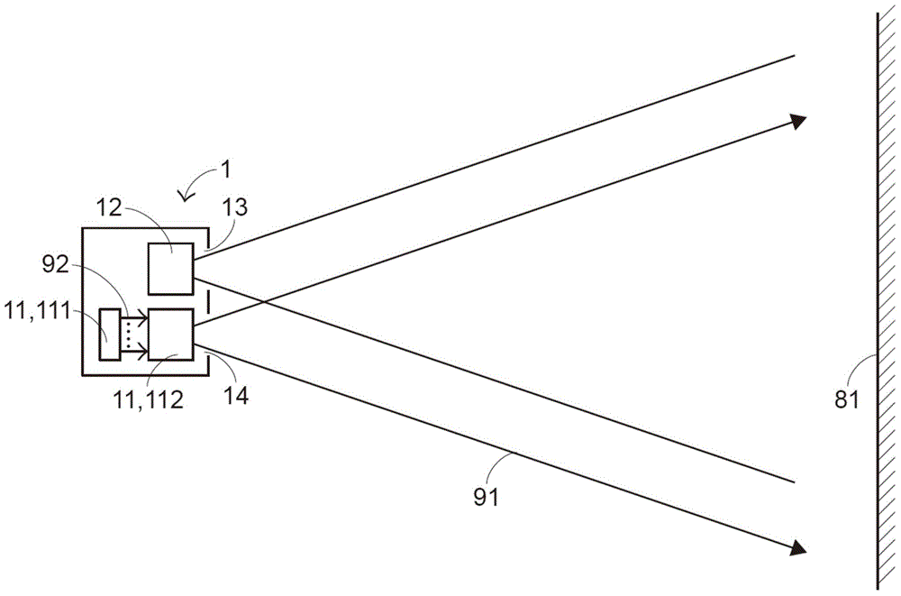
请参阅图1与图2,图1为本发明光学装置于一第一较佳实施例的结构概念示意图,图2为图1所示结构光于投射至受测表面时受测表面上所呈现的受测图案以及受测光点的概念示意图。光学装置1包括结构光产生单元11以及感应判断单元12,结构光产生单元11提供可投射至一受测表面81的一结构光91(structure light),且当结构光91投射至该受测表面81时,该受测表面81上呈现受测图案2(pattern)以及多个受测光点3。Please refer to FIG. 1 and FIG. 2 . FIG. 1 is a schematic diagram of the structure of the optical device according to a first preferred embodiment of the present invention. FIG. 2 is the appearance of the structured light shown in FIG. 1 when projected on the surface to be tested. Schematic diagram of the measured pattern and the measured light spot. The optical device 1 includes a structured light generating unit 11 and a
于本较佳实施例中,结构光产生单元11包括一发光源111以及一第一透镜组112,且发光源111可包括激光二极管(LD)、发光二极管(LED)以及有机发光二极管(OLED)中的至少一者,及/或发光源111还可包括类似于激光二极管、发光二极管以及有机发光二极管等半导体类的其它发光单元。又,发光源111是用以输出多个光束92,且光束92可为具有第一波长的光束(如可见光束)及/或具有第二波长的光束(如不可见光束或具有热感应波长区间的光束),而第一透镜组112则至少包括有相应于受测图案2以及受测光点3的光学元件(图未示,如衍射元件),并供发光源111所输出的光束92通过其中,以进而使结构光产生单元11产生输出的结构光91于投射至受测表面81时,受测表面81上可呈现受测图案2以及多个受测光点3。此外,于本较佳实施例中,受测图案2为一栅状(grid)图案,而每一受测光点3则为扩散型光束投射至受测表面81上所形成的光点,且每一扩散型光束的扩散角不限定相同。In this preferred embodiment, the structured light generating unit 11 includes a light emitting source 111 and a first lens group 112, and the light emitting source 111 may include a laser diode (LD), a light emitting diode (LED), and an organic light emitting diode (OLED) At least one of them, and/or the light-emitting source 111 may also include other light-emitting units similar to semiconductors such as laser diodes, light-emitting diodes, and organic light-emitting diodes. In addition, the light-emitting source 111 is used for outputting a plurality of
再者,感应判断单元12包括可见光感测单元(图未示)及/或不可见光感测单元(图未示),且用以感应受测表面81上所呈现的受测图案2与受测光点3,并依据所感应的受测光点3的面积大小而获得受测表面81与光学装置1之间的距离,以及依据所感应的受测图案2的一变形程度而判断受测表面81是否平坦。Furthermore, the
进一步而言,由于受测光点3为扩散型光束投射至受测表面81上所形成的光点,因此当受测表面81与光学装置1之间的距离越远,受测表面81上所呈现的受测光点3的面积就随之越大。举例来说,请参阅图3A与图3B,图3A为当光学装置1与受测表面81间隔一第一距离时感应判断单元12所感应呈现在受测表面81上的受测图案2A以及多个受测光点3A的概念示意图,图3B为当光学装置1与受测表面81间隔一第二距离时感应判断单元12所感应呈现在受测表面81上的受测图案2B以及多个受测光点3B的概念示意图。比较图3A以及图3B可知,由于图3A所示受测光点3A的面积小于图3B所示受测光点3B的面积,因此图3A所示受测表面81与光学装置1之间的距离小于图3B所示受测表面81与光学装置1之间的距离。Further, since the
显然地,根据感应判断单元12所感应的呈现在受测表面81上的受测光点3的面积,即能计算获得受测表面81与光学装置1之间的距离。而获得受测光点3的面积的方式,除了可直接计算受测光点3在感应判断单元12的感光元件(图未示)上所占的像素(pixel)值外,亦可透过受测光点3与受测图案2上的任一指定子图案的间距来判断,例如,由于图3A所示受测光点3A的面积小于图3B所示受测光点3B的面积,因此图3A所示受测光点3A与受测图案2A(栅状图案)的横线条L1的间距D1会大于图3B所示受测光点3与受测图案2B(栅状图案)的横线条L2的间距D2,由此可知,透过分别计算受测光点3A、3B与受测图案2A、2B(栅状图案)的横线条L1、L2的间距D1、D2可推得受测光点3的面积。惟,上述仅为实施例,获得受测光点3的面积的方式并不以上述为限。Obviously, the distance between the measured
接下来请参阅图3C与图3D,图3C为当受测表面81为平坦表面时感应判断单元12所感应呈现在受测表面81C上的受测图案2C以及多个受测光点3C的概念示意图,图3D为当受测表面81D为非平坦表面时感应判断单元12所感应呈现在受测表面81上的受测图案2D以及多个受测光点3D的概念示意图。比较图3C以及图3D可知,当受测表面81C为平坦表面时,受测图案2C可工整呈现在受测表面81C上,而当受测表面81D为非平坦表面时,受测图案2D会因应受测表面81D凸凹不平而产生变形。显然地,分别根据感应判断单元12所感应的呈现在受测表面81C、81D上的受测图案2C、2D的变形程度,即能判断受测表面81C、81D是否平坦;其中,变形程度可包括扭曲变形程度、歪斜变形程度以及错位变形程度中的至少一者,但不以上述为限。Next, please refer to FIGS. 3C and 3D . FIG. 3C shows the concept of the detected
请参阅图4,其为本发明光学装置于一第二较佳实施例的结构概念示意图。本较佳实施例的光学装置1’大致类似于本发明第一较佳实施例中所述者,在此即不再予以赘述,而本较佳实施例与前述第一较佳实施例不同之处在于,于第一较佳实施例中,结构光产生单元11以及感应判断单元12分别使用不同的光学路径窗口14、13,而于第二较佳实施例中,结构光产生单元11以及感应判断单元12共享单一光学路径窗口15。Please refer to FIG. 4 , which is a conceptual schematic diagram of the structure of the optical device of the present invention in a second preferred embodiment. The optical device 1 ′ of the present preferred embodiment is substantially similar to that described in the first preferred embodiment of the present invention, and will not be repeated here, and the present preferred embodiment is different from the first preferred embodiment described above. The point is that, in the first preferred embodiment, the structured light generating unit 11 and the
详言之,于第二较佳实施例中,光学装置1’更包括一光路改变元件16(如分光镜),其设置于结构光产生单元11与感应判断单元12之间,用以改变结构光产生单元11所输出的光束92的路径,使得结构光产生单元11以及感应判断单元12具有共同的光轴93,因此结构光产生单元11以及感应判断单元12可共享单一光学路径窗口15,如此一来,当光学装置1’距离受测平面81较远时,感应判断单元12更能准确地感应受测平面81上的受测图案2以及受测光点3,特别是受测平面81的边缘处(即距离光轴93较远处)。Specifically, in the second preferred embodiment, the optical device 1 ′ further includes an optical path changing element 16 (such as a beam splitter), which is disposed between the structured light generating unit 11 and the
请参阅图5,其为本发明光学装置于一第三较佳实施例的结构概念示意图。本较佳实施例的光学装置1”大致类似于本发明第二较佳实施例中所述者,在此即不再予以赘述,而本较佳实施例与前述第二较佳实施例不同之处在于,光学装置1”更包括一第二透镜组17,其位于结构光产生单元11与感应判断单元12的光学路径上,并位于光学路径窗口15的邻近处,藉以改变受测表面81上所呈现的受测图案2的大小以及感应判断单元12的视场角(FOV)。Please refer to FIG. 5 , which is a conceptual schematic diagram of the structure of the optical device of the present invention in a third preferred embodiment. The optical device 1 ″ of the present preferred embodiment is substantially similar to that described in the second preferred embodiment of the present invention, and will not be repeated here, and the present preferred embodiment is different from the second preferred embodiment described above. The point is that the optical device 1 ″ further includes a
请参阅图6,其为本发明光学装置于一第四较佳实施例的结构概念示意图。本较佳实施例的光学装置1”’大致类似于本发明第一较佳实施例中所述者,在此即不再予以赘述,而本较佳实施例与前述第一较佳实施例不同之处在于,光学装置1更包括一第二透镜组18以及一第三透镜组19,且第二透镜组18以及第三透镜组19分别位于感应判断单元12以及结构光产生单元11的光学路径上;其中,第二透镜组18用以改变感应判断单元12的视场角,而第三透镜组19用以改变受测表面81上所呈现的受测图案2的大小。Please refer to FIG. 6 , which is a schematic structural diagram of the optical device of the present invention in a fourth preferred embodiment. The optical device 1 ″' of the present preferred embodiment is substantially similar to that described in the first preferred embodiment of the present invention, which will not be repeated here, and the present preferred embodiment is different from the first preferred embodiment described above. The point is that the optical device 1 further includes a
特别说明的是,于第三较佳实施例中,第二透镜组17是可选择地于某些特定情况下才被控制移动至结构光产生单元11以及感应判断单元12的光学路径上,且于第四较佳实施例中,第二透镜组18以及第三透镜组19是可选择地于某些特定情况下才分别被控制移动至感应判断单元12以及结构光产生单元11的光学路径上。In particular, in the third preferred embodiment, the
举例来说,以第四较佳实施例而言(第三较佳实施例亦同理适用),上述特定情况可包括:当光学装置1距离受测表面81较远时,感应判断单元12能够感应到的完整的受测图案2以及所有的受测光点3,但当光学装置1距离受测表面81越来越近时,由于感应判断单元12的视场角不会改变,感应判断单元12能够感应到的范围逐渐缩小,也就是仅能够感应到的部分的受测图案2或部分的受测光点3,导致无法据以获得受测表面81与光学装置1之间的距离或判断受测表面81是否平坦的情况,此时即可透过控制第二透镜组18移动至感应判断单元12的光学路径上来增加感应判断单元12的视场角,抑或是透过控制第三透镜组19移动至结构光产生单元11的光学路径上来改变受测表面81上所呈现的受测图案2的大小,以使感应判断单元12能够感应到的完整的受测图案2以及所有的受测光点3,进而可获得受测表面81与光学装置1之间的距离以及判断受测表面81是否平坦。For example, in the case of the fourth preferred embodiment (the same applies to the third preferred embodiment), the above specific situation may include: when the optical device 1 is far away from the measured
此外,虽然上述多个较佳实施例中的受测图案皆为栅状(grid)图案,但并不以此为限,受测图案可为本技术领域普通技术人员依据实际应用需求而进行任何均等的变更设计,例如受测图案2可为图7所示的发散辐射状图案,又例如受测图案可为图8所示的斜对称状图案。In addition, although the tested patterns in the above-mentioned preferred embodiments are all grid patterns, it is not limited to this. Equally modified designs, for example, the tested
请参阅图9,其为本发明光学装置应用于空拍装置于一较佳实施例的空拍装置的底面示意图。空拍装置7的底面71设置有起降脚架72以及光学装置1,且光学装置1包括结构光产生单元11以及感应判断单元12,而结构光产生单元11以及感应判断单元12如同上述说明,在此即不再予以赘述。是以,空拍装置7可透过光学装置1而精确地获得其与欲降落的表面的距离以及欲降落的表面的平坦度,进而提升其降落质量。Please refer to FIG. 9 , which is a schematic bottom view of the optical device of the present invention applied to an aerial photography device in a preferred embodiment of the aerial photography device. The
请参阅图10,其为本发明光学装置应用于可携式电子装置的一较佳结构示意图。可携式电子装置6可为手机、平板电脑或穿戴式装置,但不以上述为限,并包括光学装置1,且光学装置1包括结构光产生单元11以及感应判断单元12,而结构光产生单元11以及感应判断单元12如同上述说明,在此即不再予以赘述。是以,可携式电子装置6可透过光学装置1而精确地获得其所欲使用的表面的距离以及平坦度。补充说明的是,图9以及图10仅为本发明光学装置1的应用实施例,本技术领域普通技术人员皆可由图9以及图10的教示而依据实际需求将本发明光学装置1应用至其它电子装置上。Please refer to FIG. 10 , which is a schematic diagram of a preferred structure of the optical device of the present invention applied to a portable electronic device. The portable electronic device 6 can be a mobile phone, a tablet computer or a wearable device, but is not limited to the above, and includes an optical device 1, and the optical device 1 includes a structured light generating unit 11 and a
根据以上的说明,侦测受测表面是否平坦以及与受测表面的距离的侦测方法可参考如图11所示的流程图。其中,侦测方法包括:步骤P1,投射一结构光至受测表面,其中,于结构光投射至受测表面时,受测表面上会呈现受测图案以及受测光点;以及步骤P2,感应受测表面上所呈现的受测图案以及受测光点,并依据所感应的受测图案的变形程度而判断受测表面是否平坦,以及依据所感应的受测光点的面积而获得与受测表面之间的距离。According to the above description, the detection method for detecting whether the tested surface is flat and the distance from the tested surface can refer to the flowchart shown in FIG. 11 . Wherein, the detection method includes: step P1, projecting a structured light to the surface to be tested, wherein, when the structured light is projected to the surface to be tested, the tested surface will present the detected pattern and the detected light spot; and step P2, Sensing the tested pattern and the tested light spot on the tested surface, and according to the deformation degree of the sensed tested pattern to determine whether the tested surface is flat, and according to the area of the sensed tested light spot to obtain the The distance between the surfaces under test.
由上述各较佳实施例的说明可知,本发明侦测方法可减少侦测受测表面是否平坦以及与受测表面的距离过程的复杂度,还能降低其所应用的电子装置的成本。补充说明的是,由于不同受测表面可能具有不同的材质,且不同的材质对热感应波长或红外线的反应不一,因此本发明的发光源还能够因应不同的材质的受测表面而提供相对应波长的光束,以进而提升判断与测量的准确性。It can be seen from the descriptions of the above preferred embodiments that the detection method of the present invention can reduce the complexity of the process of detecting whether the measured surface is flat and the distance from the measured surface, and can also reduce the cost of the electronic device to which it is applied. It is added that, since different surfaces to be tested may have different materials, and different materials have different responses to heat-induced wavelengths or infrared rays, the luminous source of the present invention can also provide a phase corresponding to the surfaces to be tested of different materials. Corresponding wavelength of light beam, so as to improve the accuracy of judgment and measurement.
以上所述仅为本发明的较佳实施例,并非用以限定本发明的权利要求范围,因此凡其它未脱离本发明所揭示的精神下所完成的等效改变或修饰,均应包含于本发明的专利保护范围内。The above descriptions are only preferred embodiments of the present invention, and are not intended to limit the scope of the claims of the present invention. Therefore, any other equivalent changes or modifications made without departing from the spirit disclosed in the present invention shall be included in the present invention. The invention is within the scope of patent protection.
Claims (20)
Priority Applications (2)
| Application Number | Priority Date | Filing Date | Title |
|---|---|---|---|
| CN201510249910.8A CN106289065B (en) | 2015-05-15 | 2015-05-15 | Detection method and optical device applying same |
| US14/959,323 US9651366B2 (en) | 2015-05-15 | 2015-12-04 | Detecting method and optical apparatus using the same |
Applications Claiming Priority (1)
| Application Number | Priority Date | Filing Date | Title |
|---|---|---|---|
| CN201510249910.8A CN106289065B (en) | 2015-05-15 | 2015-05-15 | Detection method and optical device applying same |
Publications (2)
| Publication Number | Publication Date |
|---|---|
| CN106289065A CN106289065A (en) | 2017-01-04 |
| CN106289065B true CN106289065B (en) | 2020-10-27 |
Family
ID=57631799
Family Applications (1)
| Application Number | Title | Priority Date | Filing Date |
|---|---|---|---|
| CN201510249910.8A Active CN106289065B (en) | 2015-05-15 | 2015-05-15 | Detection method and optical device applying same |
Country Status (1)
| Country | Link |
|---|---|
| CN (1) | CN106289065B (en) |
Families Citing this family (5)
| Publication number | Priority date | Publication date | Assignee | Title |
|---|---|---|---|---|
| CN107782250B (en) * | 2017-09-30 | 2020-03-06 | 维沃移动通信有限公司 | Depth information measuring method and device and mobile terminal |
| TWI673477B (en) * | 2018-06-26 | 2019-10-01 | 晶翔機電股份有限公司 | Surface slope identification device and identifying method thereof |
| CN110336938B (en) * | 2019-08-12 | 2021-02-26 | 浙江大华技术股份有限公司 | Photosensitive element, image acquisition device, lens driving method, and storage medium |
| CN111562567B (en) * | 2020-05-11 | 2021-04-30 | 北京驭光科技发展有限公司 | Obstacle detection system of mobile device, mobile device and sweeping robot |
| AU2022249790A1 (en) * | 2021-03-31 | 2023-08-31 | Keiwa Incorporated | Method for inspecting surface deformation of structure, system for inspecting surface deformation of structure, and structure protection sheet |
Family Cites Families (8)
| Publication number | Priority date | Publication date | Assignee | Title |
|---|---|---|---|---|
| WO1999058930A1 (en) * | 1998-05-14 | 1999-11-18 | Metacreations Corporation | Structured-light, triangulation-based three-dimensional digitizer |
| CA2625775A1 (en) * | 2005-10-14 | 2007-04-19 | Applied Research Associates Nz Limited | A method of monitoring a surface feature and apparatus therefor |
| US20090084852A1 (en) * | 2007-09-28 | 2009-04-02 | Igor Vinogradov | Aiming pattern indicative of optimum working distance in imaging reader and method |
| GB0921461D0 (en) * | 2009-12-08 | 2010-01-20 | Qinetiq Ltd | Range based sensing |
| US9131136B2 (en) * | 2010-12-06 | 2015-09-08 | Apple Inc. | Lens arrays for pattern projection and imaging |
| EP2511656A1 (en) * | 2011-04-14 | 2012-10-17 | Hexagon Technology Center GmbH | Measuring system for determining the 3D coordinates of an object surface |
| US9245307B2 (en) * | 2011-06-01 | 2016-01-26 | Empire Technology Development Llc | Structured light projection for motion detection in augmented reality |
| CN204271437U (en) * | 2014-10-31 | 2015-04-15 | 高准精密工业股份有限公司 | Surface Fixed Diffractive Optical Laser Module |
-
2015
- 2015-05-15 CN CN201510249910.8A patent/CN106289065B/en active Active
Also Published As
| Publication number | Publication date |
|---|---|
| CN106289065A (en) | 2017-01-04 |
Similar Documents
| Publication | Publication Date | Title |
|---|---|---|
| CN106289065B (en) | Detection method and optical device applying same | |
| CN102841710B (en) | sensing method and device | |
| TWI570387B (en) | Image ranging system, light source module and image sensing module | |
| US8982101B2 (en) | Optical touch system and optical touch-position detection method | |
| WO2013035553A1 (en) | User interface display device | |
| CN102822623A (en) | Information acquisition device, projection device, and object detection device | |
| TW201710642A (en) | Structured light generating apparatus, measuring system and method thereof | |
| CN110462688B (en) | Three-dimensional profile determination system and method using model-based peak selection | |
| JP2015197744A5 (en) | ||
| CN106289092B (en) | Optical device and light-emitting device thereof | |
| CN110603482A (en) | Backlight substrate, manufacturing method thereof and display device | |
| US10281997B2 (en) | Identification of an object on a touch-sensitive surface | |
| CN110728713B (en) | Test method and test system | |
| TWM509339U (en) | Optical device and its illuminating device | |
| US9651366B2 (en) | Detecting method and optical apparatus using the same | |
| TW201631456A (en) | Gesture sensing module, method, and electronic apparatus thereof | |
| TWI651511B (en) | Detection method and optical device using the same | |
| CN110809705A (en) | Proximity sensor and method of operating the same | |
| CN107743628A (en) | The luminous structured light in LED faces | |
| US9652081B2 (en) | Optical touch system, method of touch detection, and computer program product | |
| US11575875B2 (en) | Multi-image projector and electronic device having multi-image projector | |
| TW201435687A (en) | Touch control apparatus and associated selecting method | |
| CN102063228A (en) | Optical sensing system and touch screen applying same | |
| CN105988575A (en) | Gesture sensing module, method and electronic device thereof | |
| US9860519B2 (en) | Method for correcting image phase |
Legal Events
| Date | Code | Title | Description |
|---|---|---|---|
| C06 | Publication | ||
| PB01 | Publication | ||
| SE01 | Entry into force of request for substantive examination | ||
| SE01 | Entry into force of request for substantive examination | ||
| GR01 | Patent grant | ||
| GR01 | Patent grant |