CN106239352B - Grinding device - Google Patents
Grinding device Download PDFInfo
- Publication number
- CN106239352B CN106239352B CN201610382395.5A CN201610382395A CN106239352B CN 106239352 B CN106239352 B CN 106239352B CN 201610382395 A CN201610382395 A CN 201610382395A CN 106239352 B CN106239352 B CN 106239352B
- Authority
- CN
- China
- Prior art keywords
- light
- fiber
- wafer
- polishing
- beam splitter
- Prior art date
- Legal status (The legal status is an assumption and is not a legal conclusion. Google has not performed a legal analysis and makes no representation as to the accuracy of the status listed.)
- Active
Links
Images


Classifications
-
- B—PERFORMING OPERATIONS; TRANSPORTING
- B24—GRINDING; POLISHING
- B24B—MACHINES, DEVICES, OR PROCESSES FOR GRINDING OR POLISHING; DRESSING OR CONDITIONING OF ABRADING SURFACES; FEEDING OF GRINDING, POLISHING, OR LAPPING AGENTS
- B24B37/00—Lapping machines or devices; Accessories
- B24B37/04—Lapping machines or devices; Accessories designed for working plane surfaces
- B24B37/07—Lapping machines or devices; Accessories designed for working plane surfaces characterised by the movement of the work or lapping tool
- B24B37/10—Lapping machines or devices; Accessories designed for working plane surfaces characterised by the movement of the work or lapping tool for single side lapping
-
- B—PERFORMING OPERATIONS; TRANSPORTING
- B24—GRINDING; POLISHING
- B24B—MACHINES, DEVICES, OR PROCESSES FOR GRINDING OR POLISHING; DRESSING OR CONDITIONING OF ABRADING SURFACES; FEEDING OF GRINDING, POLISHING, OR LAPPING AGENTS
- B24B37/00—Lapping machines or devices; Accessories
- B24B37/005—Control means for lapping machines or devices
- B24B37/013—Devices or means for detecting lapping completion
-
- H10P52/00—
-
- B—PERFORMING OPERATIONS; TRANSPORTING
- B24—GRINDING; POLISHING
- B24B—MACHINES, DEVICES, OR PROCESSES FOR GRINDING OR POLISHING; DRESSING OR CONDITIONING OF ABRADING SURFACES; FEEDING OF GRINDING, POLISHING, OR LAPPING AGENTS
- B24B37/00—Lapping machines or devices; Accessories
- B24B37/11—Lapping tools
- B24B37/20—Lapping pads for working plane surfaces
- B24B37/205—Lapping pads for working plane surfaces provided with a window for inspecting the surface of the work being lapped
-
- B—PERFORMING OPERATIONS; TRANSPORTING
- B24—GRINDING; POLISHING
- B24B—MACHINES, DEVICES, OR PROCESSES FOR GRINDING OR POLISHING; DRESSING OR CONDITIONING OF ABRADING SURFACES; FEEDING OF GRINDING, POLISHING, OR LAPPING AGENTS
- B24B49/00—Measuring or gauging equipment for controlling the feed movement of the grinding tool or work; Arrangements of indicating or measuring equipment, e.g. for indicating the start of the grinding operation
- B24B49/12—Measuring or gauging equipment for controlling the feed movement of the grinding tool or work; Arrangements of indicating or measuring equipment, e.g. for indicating the start of the grinding operation involving optical means
-
- H10P52/402—
-
- H10P74/203—
-
- H10P74/27—
Landscapes
- Engineering & Computer Science (AREA)
- Mechanical Engineering (AREA)
- Manufacturing & Machinery (AREA)
- Mechanical Treatment Of Semiconductor (AREA)
- Computer Hardware Design (AREA)
- Microelectronics & Electronic Packaging (AREA)
- Power Engineering (AREA)
- Physics & Mathematics (AREA)
- Condensed Matter Physics & Semiconductors (AREA)
- General Physics & Mathematics (AREA)
- Constituent Portions Of Griding Lathes, Driving, Sensing And Control (AREA)
- Finish Polishing, Edge Sharpening, And Grinding By Specific Grinding Devices (AREA)
Abstract
本发明提供一种不使用光纤的光程切换器,而使用多个光传感器能够测定晶圆膜厚的研磨装置,该研磨装置具备:具有配置于研磨台(3)中不同位置的多个顶端(34a、34b)的投光光纤(34);按照波长分解来自晶圆W的反射光,并测定各波长的反射光强度的分光器(26);具有配置于研磨台(3)中不同位置的多个顶端(50a、50b)的受光光纤50);以及生成表示反射光的强度与波长的关系的分光波形的处理部(27)。处理部(27)根据分光波形确定膜厚。

The present invention provides a polishing apparatus capable of measuring the film thickness of a wafer by using a plurality of optical sensors without using an optical path switch of an optical fiber. The polishing apparatus is provided with a plurality of tips arranged at different positions in a polishing table (3). Light projecting optical fibers (34) of (34a, 34b); a beam splitter (26) for decomposing the reflected light from the wafer W according to wavelength and measuring the reflected light intensity of each wavelength; having different positions arranged in the polishing table (3) a light-receiving optical fiber 50) at a plurality of tips (50a, 50b); and a processing unit (27) that generates a spectral waveform representing the relationship between the intensity and wavelength of the reflected light. The processing unit (27) determines the film thickness based on the spectral waveform.
Description
技术领域technical field
本发明涉及一种研磨表面形成有膜的晶圆的研磨装置,特别涉及通过分析在来自晶圆的反射光中包含的光学信息,能够检测晶圆的膜厚的研磨装置。The present invention relates to a polishing apparatus for polishing a wafer on which a film is formed, and more particularly, to a polishing apparatus capable of detecting the film thickness of the wafer by analyzing optical information contained in reflected light from the wafer.
背景技术Background technique
半导体组件的制造步骤中包含:研磨二氧化硅(SiO2)等绝缘膜的工序;以及研磨铜、钨等金属膜的工序等各种工序。在背面照射型CMOS传感器及硅贯通电极(TSV)的制造工序,除了绝缘膜以及金属膜的研磨工序之外,还包含研磨硅层(硅晶圆)的工序。晶圆的研磨在构成其表面的膜(绝缘膜、金属膜、硅层等)的厚度达到指定的目标值时结束。The manufacturing process of the semiconductor device includes various processes such as a process of grinding an insulating film such as silicon dioxide (SiO 2 ) and a process of grinding a metal film such as copper and tungsten. The manufacturing process of the backside illuminated CMOS sensor and the through-silicon electrode (TSV) includes a process of grinding a silicon layer (silicon wafer) in addition to the grinding process of the insulating film and the metal film. The polishing of the wafer ends when the thickness of the film (insulating film, metal film, silicon layer, etc.) constituting the surface reaches a specified target value.
晶圆的研磨使用研磨装置而进行。图13为表示研磨装置的一个实例的示意图。一般而言,研磨装置具备:支承研磨垫201并可旋转的研磨台202;在研磨台202上的研磨垫201上推压晶圆W的研磨头205;在研磨垫201上供给研磨液(浆液)的研磨液供给喷嘴206;以及测定晶圆W膜厚的膜厚测定装置210。The polishing of the wafer is performed using a polishing apparatus. FIG. 13 is a schematic diagram showing an example of a polishing apparatus. In general, the polishing apparatus includes: a polishing table 202 that supports the
图13所示的膜厚测定装置210为光学式膜厚测定装置。该膜厚测定装置210具备:发出光的光源212;连接于光源212的投光光纤215;在研磨台202中的不同位置配置有顶端的第一光纤216以及第二光纤217;将第一光纤216以及第二光纤217中的任何一方选择性地连接于投光光纤215的第一光程切换器220;测定来自晶圆W的反射光强度的分光器222;连接于分光器222的受光光纤224;在研磨台202中的不同位置配置有顶端的第三光纤227及第四光纤228;以及将第三光纤227以及第四光纤228中任何一方选择性地连接于受光光纤224的第二光程切换器230。The film
第一光纤216的顶端以及第三光纤227的顶端构成第一光传感器234,第二光纤217的顶端以及第四光纤228的顶端构成第二光传感器235。这些第一光传感器234以及第二光传感器235被配置于研磨台202中的不同位置,在研磨台202旋转的同时,第一光传感器234以及第二光传感器235交互地穿过晶圆W。第一光传感器234以及第二光传感器235导光于晶圆W上,并接收来自晶圆W的反射光。反射光通过第三光纤227或第四光纤228传达至受光光纤224,进一步通过受光光纤224而传达至分光器222。分光器222按照波长分解反射光,测定反射光的各波长强度。处理部240连接于分光器222,从反射光强度的测定值生成分光波形(光谱)进而从分光波形确定晶圆W的膜厚。The top end of the first
图14为表示第一光程切换器220的示意图。第一光程切换器220具备使第一光纤216以及第二光纤217的端部移动的压电致动器244。由于该压电致动器244使第一光纤216以及第二光纤217的端部移动,第一光纤216以及第二光纤217中的一方连接于投光光纤215。虽然未图示,但第二光程切换器230也具有相同构成。FIG. 14 is a schematic diagram showing the first
第一光程切换器220以及第二光程切换器230在第一光传感器234穿过晶圆W期间,将第一光纤216以及第三光纤227分别连接于投光光纤215以及受光光纤224,在第二光传感器235穿过晶圆W期间,将第二光纤217以及第四光纤228分别连接于投光光纤215以及受光光纤224。如此,由于在研磨台202旋转一周期间,第一光程切换器220及第二光程切换器230工作,因此,分光器222能够分别处理第一光传感器234以及第二光传感器235所接收的反射光。The first
现有技术文献prior art literature
专利文献Patent Literature
专利文献1日本特开2012-138442号公报
专利文献2日本特表2014-504041号公报Patent Document 2 Japanese Patent Publication No. 2014-504041
发明内容SUMMARY OF THE INVENTION
发明要解决的问题Invention to solve problem
但是,由于第一光程切换器220以及第二光程切换器230为机械的切换装置,因此长期持续使用时会发生不良状况,当第一光程切换器220或第二光程切换器230发生不良状况时,从第一光传感器234以及第二光传感器235导入分光器222的反射光强度改变,导致处理部240确定的膜厚发生变动。However, since the first
本发明是鉴于上述情形而做出的,其目的在于提供一种不使用光纤的光程切换器,而使用多个光传感器能够测定晶圆膜厚的研磨装置。The present invention has been made in view of the above-mentioned circumstances, and an object thereof is to provide a polishing apparatus capable of measuring the film thickness of a wafer using a plurality of optical sensors without using an optical path switch.
解决问题的技术手段technical solutions to problems
为了达成上述目的,本发明的一种方式为一种研磨装置,其特征在于,其具备:研磨台,其支承研磨垫;研磨头,其将晶圆推压于所述研磨垫;光源,其发出光;投光光纤,其具有配置于所述研磨台中的不同位置的多个顶端;分光器,其将来自晶圆的反射光按照波长分解,并测定各波长的反射光强度;受光光纤,其具有配置于所述研磨台中的所述不同位置的多个顶端;以及处理部,其生成显示所述反射光强度与波长的关系的分光波形;所述投光光纤连接于所述光源,将从所述光源发出的光引导于晶圆表面,所述受光光纤连接于所述分光器,将来自晶圆的反射光引导至所述分光器,所述处理部依据所述分光波形确定膜厚。In order to achieve the above object, one aspect of the present invention is a polishing apparatus, which is characterized by comprising: a polishing table supporting a polishing pad; a polishing head for pressing a wafer against the polishing pad; a light source for Emitting light; light-projecting fiber, which has a plurality of tips arranged at different positions in the grinding table; beam splitter, which decomposes the reflected light from the wafer according to wavelength, and measures the reflected light intensity of each wavelength; light-receiving fiber, It has a plurality of tips arranged at the different positions in the grinding table; and a processing part that generates a spectral waveform showing the relationship between the reflected light intensity and the wavelength; the light projection fiber is connected to the light source, and The light emitted from the light source is guided to the surface of the wafer, the light-receiving fiber is connected to the spectroscope, and the reflected light from the wafer is guided to the spectroscope, and the processing unit determines the film thickness based on the spectral waveform .
本发明优选方式的特征在于,所述投光光纤具有:投光主干光纤,其连接于所述光源;以及第一投光分支光纤及第二投光分支光纤,其从所述投光主干光纤分支,所述受光光纤具有:受光主干光纤,其连接于所述分光器;以及第一受光分支光纤及第二受光分支光纤,其从所述受光主干光纤分支。A preferred mode of the present invention is characterized in that the light-projecting fiber has: a light-projecting trunk fiber connected to the light source; and a first light-projecting branch fiber and a second light-projecting branch fiber, which are connected from the light-projecting trunk fiber The light-receiving fiber includes: a light-receiving trunk fiber connected to the optical splitter; and a first light-receiving branch fiber and a second light-receiving branch fiber branched from the light-receiving trunk fiber.
本发明优选的方式的特征在于,所述投光光纤的顶端以及所述受光光纤的顶端导光于晶圆上,构成接收来自晶圆的反射光的第一光传感器以及第二光传感器,所述第二光传感器相对于所述研磨台的中心配置于所述第一光传感器的相反侧。A preferred mode of the present invention is characterized in that the tip of the light-projecting fiber and the tip of the light-receiving fiber guide light on the wafer to constitute a first photosensor and a second photosensor that receive reflected light from the wafer, so that the The second photosensor is disposed on the opposite side of the first photosensor with respect to the center of the polishing table.
本发明优选方式的特征在于,进一步具备校正用光源,其发出具有特定波长的光,所述校正用光源通过校正用光纤而连接于所述分光器。A preferred aspect of the present invention is characterized by further comprising a light source for calibration that emits light having a specific wavelength, and the light source for calibration is connected to the spectroscope through an optical fiber for calibration.
本发明优选方式的特征在于,所述光源由第一光源以及第二光源构成。In a preferred embodiment of the present invention, the light source is composed of a first light source and a second light source.
本发明优选方式的特征在于,所述第一光源以及所述第二光源发出相同波长范围的光。In a preferred embodiment of the present invention, the first light source and the second light source emit light in the same wavelength range.
本发明优选方式的特征在于,所述第一光源以及所述第二光源发出不同波长范围的光。A preferred embodiment of the present invention is characterized in that the first light source and the second light source emit light in different wavelength ranges.
本发明优选方式的特征在于,所述分光器由第一分光器以及第二分光器构成。In a preferred embodiment of the present invention, the spectroscope includes a first spectroscope and a second spectroscope.
本发明优选方式的特征在于,所述第一分光器以及所述第二分光器以在不同波长范围测定反射光强度的方式构成。In a preferred embodiment of the present invention, the first spectroscope and the second spectroscope are configured to measure the reflected light intensity in different wavelength ranges.
本发明优选方式的特征在于,所述处理部对所述分光波形进行傅里叶变换处理,生成表示膜厚与频率成分强度的关系的频率光谱,确定比临界值大的频率成分强度的峰值,并确定对应于该峰值的膜厚。A preferred embodiment of the present invention is characterized in that the processing unit performs Fourier transform processing on the spectral waveform, generates a frequency spectrum representing the relationship between the film thickness and the intensity of the frequency component, and identifies a peak of the intensity of the frequency component larger than a threshold value, And determine the film thickness corresponding to this peak.
发明的效果effect of invention
来自晶圆的反射光仅在投光光纤以及受光光纤的顶端存在于晶圆下方时才引导至分光器。换而言之,投光光纤以及受光光纤的顶端不在晶圆下方时,引导至分光器的光强度极低。即,除了来自晶圆的反射光以外的光不被用于确定膜厚。因此,能够不设置光程切换器而确定膜厚。The reflected light from the wafer is guided to the beam splitter only when the tips of the light-emitting fiber and the light-receiving fiber exist under the wafer. In other words, when the tips of the light-emitting fiber and the light-receiving fiber are not under the wafer, the light intensity guided to the beam splitter is extremely low. That is, light other than reflected light from the wafer is not used to determine the film thickness. Therefore, the film thickness can be determined without providing an optical path switch.
附图说明Description of drawings
图1为表示本发明一种实施方式涉及的研磨装置的图。FIG. 1 is a diagram showing a polishing apparatus according to an embodiment of the present invention.
图2为表示研磨垫以及研磨台的俯视图。2 is a plan view showing a polishing pad and a polishing table.
图3为表示连接于光源的投光光纤的放大图。FIG. 3 is an enlarged view showing a light projecting fiber connected to a light source.
图4为表示连接于分光器的受光光纤的放大图。FIG. 4 is an enlarged view showing a light-receiving fiber connected to a spectroscope.
图5为用于说明光学式膜厚测定器的原理的示意图。FIG. 5 is a schematic diagram for explaining the principle of the optical film thickness measuring device.
图6为表示分光波形的一个实例的图形。FIG. 6 is a graph showing an example of a spectral waveform.
图7为表示对图6所示的分光波形进行傅里叶变换处理而获得的频率光谱图形。FIG. 7 is a graph showing a frequency spectrum obtained by subjecting the spectral waveform shown in FIG. 6 to Fourier transform processing.
图8为表示投光光纤的顶端以及受光光纤的顶端不在晶圆下方时生成的频率光谱图形。FIG. 8 is a graph showing the frequency spectrum generated when the tip of the light-emitting fiber and the tip of the light-receiving fiber are not under the wafer.
图9为表示具备第一光源与第二光源的实施方式的示意图。FIG. 9 is a schematic diagram showing an embodiment including a first light source and a second light source.
图10为表示除了光源之外,进一步具备发出具有特定波长的光的校正用光源的实施方式的示意图。FIG. 10 is a schematic diagram showing an embodiment further including a light source for calibration that emits light having a specific wavelength in addition to the light source.
图11为表示具备第一分光器与第二分光器的实施方式的示意图。FIG. 11 is a schematic diagram showing an embodiment including a first beam splitter and a second beam splitter.
图12为表示设有第一光源及第二光源、第一分光器及第二分光器的实施方式的示意图。12 is a schematic diagram showing an embodiment in which a first light source and a second light source, and a first beam splitter and a second beam splitter are provided.
图13为表示研磨装置的一个实例的示意图。FIG. 13 is a schematic diagram showing an example of a polishing apparatus.
图14为表示图13所示的第一光程切换器的示意图。FIG. 14 is a schematic diagram showing the first optical path switch shown in FIG. 13 .
具体实施方式Detailed ways
以下,参照附图说明本发明的实施方式。图1为表示本发明一实施方式涉及的研磨装置的图。如图1所示,研磨装置具备:支承研磨垫1的研磨台3;保持晶圆W并将晶圆W推压于研磨台3上的研磨垫1的研磨头5;用于在研磨垫1上供给研磨液(例如浆液)的研磨液供给喷嘴10;以及控制晶圆W研磨的研磨控制部12。Hereinafter, embodiments of the present invention will be described with reference to the accompanying drawings. FIG. 1 is a view showing a polishing apparatus according to an embodiment of the present invention. As shown in FIG. 1 , the polishing apparatus includes: a polishing table 3 supporting the
研磨台3经由台轴3a而连接于配置在其下方的台马达19,研磨台3通过该台马达19可在箭头指示的方向旋转。在该研磨台3的上表面贴合有研磨垫1,研磨垫1的上表面构成研磨晶圆W的研磨面1a。研磨头5连接于研磨头轴杆16的下端。研磨头5以能够由真空吸引而在其下面保持晶圆W的方式构成。研磨头轴杆16能够经由未图示的上下运动机构而上下运动。The grinding table 3 is connected to a
晶圆W的研磨如下进行。使研磨头5以及研磨台3分别按箭头指示的方向旋转,从研磨液供给喷嘴10供给研磨液(浆液)至研磨垫1上。在该状态下,研磨头5将晶圆W推压于研磨垫1的研磨面1a上。晶圆W表面由于研磨液中包含的研磨粒的机械作用与研磨液的化学作用而被研磨。The polishing of the wafer W is performed as follows. The polishing
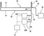
研磨装置具备测定晶圆W膜厚的光学式膜厚测定器(膜厚测定装置)25。该光学式膜厚测定器25具备:发出光的光源30;具有被配置于研磨台3中不同位置的多个顶端34a、34b的投光光纤34;按照波长分解来自晶圆W的反射光,并测定各波长的反射光强度的分光器26;具有被配置于研磨台3中所述不同位置的多个顶端50a、50b的受光光纤50;以及生成表示反射光强度与波长的关系的分光波形的处理部27。处理部27连接于研磨控制部12。The polishing apparatus includes an optical film thickness measuring device (film thickness measuring device) 25 for measuring the film thickness of the wafer W. The optical film
投光光纤34连接于光源30,并以使从光源30发出的光引导于晶圆W表面的方式配置。受光光纤50连接于分光器26,并以将来自晶圆W的反射光引导至分光器26的方式配置。投光光纤34的一个顶端34a与受光光纤50的一个顶端50a彼此相邻,这些顶端34a、50a构成第一光传感器61。投光光纤34的另一个顶端34b与受光光纤50的另一个顶端50b彼此相邻,这些顶端34b、50b构成第二光传感器62。研磨垫1具有位于第一光传感器61以及第二光传感器62上方的通孔1b、1c,第一光传感器61以及第二光传感器62可通过这些通孔1b、1c而导光于研磨垫1上的晶圆W,并接收来自晶圆W的反射光。The
图2为表示研磨垫1以及研磨台3的俯视图。第一光传感器61以及第二光传感器62位于从研磨台3中心起不同的距离,且在研磨台3的周向彼此分离而被配置。图2所示的实施方式为第二光传感器62相对于对研磨台3的中心被配置于第一光传感器61的相反侧。第一光传感器61以及第二光传感器62在研磨台3每旋转一周描绘不同的轨迹并交互穿过晶圆W。具体而言,第一光传感器61穿过晶圆W的中心,第二光传感器62仅穿过晶圆W的边缘部。第一光传感器61以及第二光传感器62交互地导光于晶圆W,并接收来自晶圆W的反射光。FIG. 2 is a plan view showing the
图3为表示连接于光源30的投光光纤34的放大图。投光光纤34由被捆束具31捆束的多条股线光纤32而构成。投光光纤34具有:连接于光源30的投光主干光纤35;以及从投光主干光纤35分支的第一投光分支光纤36及第二投光分支光纤37。FIG. 3 is an enlarged view showing the light projecting
图4为表示连接于分光器26的受光光纤50的放大图。受光光纤50也同样地被由捆束具51捆束的多条股线光纤52而构成。受光光纤50具有:连接于分光器26的受光主干光纤55;以及从受光主干光纤55分支的第一受光分支光纤56及第二受光分支光纤57。FIG. 4 is an enlarged view showing the light-receiving
投光光纤34的顶端34a、34b由第一投光分支光纤36及第二投光分支光纤37的顶端构成,这些顶端34a、34b如上所述位于研磨台3中。受光光纤50的顶端50a、50b由第一受光分支光纤56及第二受光分支光纤57的顶端构成,这些顶端50a、50b也位于研磨台3中。The
在图3以及图4所示的实施方式,1条主干光纤分支成2条分支光纤,不过,也可以通过增加股线光纤,而分支成3条以上的分支光纤。再者,能够通过增加股线光纤而轻易地增大光纤直径。此种由多条股线光纤构成的光纤具备容易弯曲,且不易折断的优点。In the embodiments shown in FIGS. 3 and 4 , one trunk fiber is branched into two branch fibers, but it may be branched into three or more branch fibers by adding stranded fibers. Furthermore, the fiber diameter can be easily increased by adding stranded fibers. Such an optical fiber composed of a plurality of stranded optical fibers has the advantages of being easy to bend and not easily broken.
晶圆W研磨中,从投光光纤34向晶圆W照射光,并由受光光纤50接收来自晶圆W的反射光。分光器26按照波长分解反射光,在整个指定的波长范围测定各波长的反射光强度,并将获得的光强度数据传送至处理部27。该光强度资料为反映晶圆W膜厚的光学信号,由反射光的强度及对应的波长构成。处理部27从光强度数据生成表示各波长的光强度的分光波形。During polishing of the wafer W, light is irradiated to the wafer W from the
图5为用于说明光学式膜厚测定器25的原理的示意图。在图5所示的实例,晶圆W具有:下层膜;以及形成于其上的上层膜。上层膜例如为硅层或绝缘膜等容许光透过的膜。照射于晶圆W的光在媒介(图5的例中为水)与上层膜的界面、及上层膜与下层膜的界面反射,被这些界面反射的光波彼此干涉。该光波干涉的方式根据上层膜的厚度(即光程长)而变化。因而,由来自晶圆W的反射光而生成的分光波形随上层膜的厚度而变化。FIG. 5 is a schematic diagram for explaining the principle of the optical film
分光器26按照波长分解反射光,对各波长测定反射光强度。处理部27从分光器26获得的反射光强度数据(光学信号)生成分光波形。该分光波形作为表示光波长与强度的关系的线图形来表示。光强度也可作为后述的相对反射率等的相对值来表示。The
图6为表示分光波形的一个实例的图形。图6中,纵轴表示显示来自晶圆W的反射光强度的相对反射率,横轴表示反射光的波长。所谓相对反射率为表示反射光强度的指标值,且为光强度与指定的基准强度之比。各波长中通过将光强度(实测强度)除以指定的基准强度,能够从实测强度除去装置的光学系统、光源固有强度的偏差等不需要的噪声。FIG. 6 is a graph showing an example of a spectral waveform. In FIG. 6 , the vertical axis represents the relative reflectance indicating the intensity of reflected light from the wafer W, and the horizontal axis represents the wavelength of the reflected light. The so-called relative reflectivity is an index value indicating the intensity of reflected light, and is the ratio of the light intensity to a specified reference intensity. By dividing the light intensity (actually measured intensity) by a predetermined reference intensity for each wavelength, unnecessary noises such as variations in the optical system of the device and the intensity of the light source can be removed from the actual measured intensity.
基准强度为对于各波长预先取得的强度,且对于各波长算出相对反射率。具体而言,通过将各波长的光强度(实测强度)除以对应的基准强度而求出相对反射率。基准强度例如通过直接测定从膜厚传感器发出的光强度,或是从膜厚传感器照射光至镜上,通过测定来自镜的反射光强度而获得。或是,基准强度也可作为在水存在下水研磨尚未形成膜的硅晶圆(裸晶圆)时获得的光强度。在实际的研磨,从实测强度减去黑电平(dark level)(在遮蔽光条件下获得的背景强度)求出修正实测强度,再从基准强度减去上述黑电平求出修正基准强度,而后,通过将修正实测强度除以修正基准强度而求出相对反射率。具体而言,可使用以下公式求出相对反射率R(λ)。The reference intensity is an intensity obtained in advance for each wavelength, and the relative reflectance is calculated for each wavelength. Specifically, the relative reflectance is obtained by dividing the light intensity (actually measured intensity) of each wavelength by the corresponding reference intensity. The reference intensity is obtained, for example, by directly measuring the intensity of light emitted from the film thickness sensor, or by irradiating light from the film thickness sensor to the mirror and measuring the intensity of reflected light from the mirror. Alternatively, the reference intensity may be used as the light intensity obtained when water-polishing a silicon wafer (bare wafer) that has not yet formed a film in the presence of water. In actual polishing, the corrected actual intensity is obtained by subtracting the dark level (the background intensity obtained under the shielded light condition) from the measured intensity, and the corrected reference intensity is obtained by subtracting the above-mentioned black level from the reference intensity. Then, the relative reflectance is obtained by dividing the corrected measured intensity by the corrected reference intensity. Specifically, the relative reflectance R(λ) can be obtained using the following formula.
[数学式1][Mathematical formula 1]

其中,λ为波长,E(λ)为从晶圆反射的波长λ的光强度,B(λ)为波长λ的基准强度,D(λ)为在遮断光条件下所取得的波长λ的背景强度(黑电平)。where λ is the wavelength, E(λ) is the light intensity of the wavelength λ reflected from the wafer, B(λ) is the reference intensity of the wavelength λ, and D(λ) is the background of the wavelength λ obtained under the condition of blocking light Intensity (black level).
处理部27对分光波形进行傅里叶变换处理(例如,高速傅里叶变换处理)而生成频率光谱,并从频率光谱确定晶圆W的膜厚。图7为表示对图6所示的分光波形进行傅里叶变换处理而获得的频率光谱的图形。图7中,纵轴表示分光波形中包含的频率成分的强度,横轴表示膜厚。频率成分的强度相当于作为正弦波而表示的频率成分的振幅。分光波形中包含的频率成分使用指定的关系公式变换成膜厚,生成表示如图7所示的膜厚与频率成分强度的关系的频率光谱。上述指定的关系公式为将频率成分作为变量来表示膜厚的一次函数,且能够根据膜厚的实测结果或光学性膜厚测定模拟等求出。The
图7所示的图形中,频率成分强度的峰值在膜厚t1出现。换而言之,膜厚t1时,频率成分的强度最大。即,该频率光谱表示膜厚为t1。如此,处理部27确定对应于频率成分强度峰值的膜厚。In the graph shown in FIG. 7, the peak of the frequency component intensity appears at the film thickness t1. In other words, when the film thickness is t1, the intensity of the frequency component is the largest. That is, the frequency spectrum indicates that the film thickness is t1. In this way, the
处理部27将膜厚t1作为膜厚测定值而输出至研磨控制部12。研磨控制部12依据从处理部27送来的膜厚t1控制研磨动作(例如,研磨结束动作)。例如,研磨控制部12于膜厚t1达到规定的目标值时结束晶圆W的研磨。The
本实施方式的膜厚测定装置25与图13所示的膜厚测定装置210不同,不具用于将多条分支光纤选择性连接于主干光纤的光程切换器。即,投光主干光纤35始终连接于第一投光分支光纤36以及第二投光分支光纤37。同样地,受光主干光纤55始终连接于第一受光分支光纤56以及第二受光分支光纤57。Unlike the film
第二光传感器62相对于研磨台3的中心被配置于第一光传感器61的相反侧。因此,晶圆W研磨中,在研磨台3每旋转一周,第一光传感器61以及第二光传感器62交互地穿过晶圆W。分光器26通过受光光纤50的第一受光分支光纤56及第二受光分支光纤57随时接收光。但是,投光光纤34以及受光光纤50的顶端34a、34b、50a、50b不在晶圆W下方时,分光器26接收的光强度极低。因此,处理部27为了区别来自晶圆W的反射光与其他光,而如图7所示,在处理部27中预先存储了有关频率成分强度的临界值。The
投光光纤34以及受光光纤50的顶端34a、34b、50a、50b不在晶圆W下方时,入射于分光器26的光强度低。此时,频率光谱中包含的整个频率成分的强度降低。图8为表示投光光纤34的顶端以及受光光纤50的顶端不在晶圆W下方时所生成的频率光谱的图形。如图8所示,整个频率成分的强度的临界值也低。因此,该频率光谱不能用于确定膜厚。When the
反之,如图7所示,从来自晶圆W的反射光所生成的频率光谱包含比临界值大的频率成分的强度,且频率成分强度的峰值比临界值大。因此,该频率光谱能够用于确定膜厚。On the contrary, as shown in FIG. 7 , the frequency spectrum generated from the reflected light from the wafer W includes the intensity of frequency components larger than the threshold value, and the peak value of the intensity of the frequency components is larger than the threshold value. Therefore, the frequency spectrum can be used to determine the film thickness.
如此,处理部27通过将频率光谱中包含的频率成分强度与临界值比较,即可区别来自晶圆W的反射光和其他光。进一步地,由于第一光传感器61以及第二光传感器62交互穿过晶圆W,因此,第一光传感器61以及第二光传感器62接收的反射光不重叠。因此,不需要设置光程切换器。上述实施方式的膜厚测定除了在晶圆W研磨中之外,也可在晶圆W研磨前和/或研磨后进行。In this way, the
图9为表示具备第一光源30A与第二光源30B的实施方式的示意图。如图9所示,本实施方式的光源30由第一光源30A与第二光源30B构成。投光光纤34连接于第一光源30A与第二光源30B两者。即,投光主干光纤35具有2个输入端子线35a、35b,这些输入端子线35a、35b分别连接于第一光源30A与第二光源30B。FIG. 9 is a schematic diagram showing an embodiment including a first
第一光源30A与第二光源30B也可为具有不同构成的光源。例如,第一光源30A由卤素灯构成,第二光源30B由发光敏二极管构成。卤素灯发出的光的波长范围广(例如,300nm~1300nm),且寿命短(约2000小时),而发光敏二极管发出的光的波长范围窄(例如900nm~1000nm),且寿命长(约10000小时)。本实施方式可以依据晶圆W的膜种类适当选择第一光源30A或第二光源30B的任意一个。也可以使用氙灯、重氢灯、激光器等其他类型的光源。The first
第一光源30A与第二光源30B也可以为具有发出相同波长范围的光的相同构成的光源。例如,也可以第一光源30A及第二光源30B两者都使用卤素灯。卤素灯的寿命比较短,约为2000小时。根据本实施方式,在第一光源30A的光量降低时,能够通过切换成第二光源30B,延长膜厚测定装置25的使用寿命。进一步地,当第二光源30B的光量也降低时,将第一光源30A及第二光源30B两者更换成新品。根据本实施方式,由于能够通过一次更换作业实现两倍寿命,因此能够缩短使研磨装置运转停止的时间。The first
图10为表示除光源30之外,进一步具备发出具有特定波长的光的校正用光源60的实施方式的示意图。校正用光源60以校正用光纤63连接于分光器26。校正用光纤63也可以由受光光纤50的一部分构成。即,校正用光纤63也可以由从受光主干光纤55分支的第三受光分支光纤构成。FIG. 10 is a schematic diagram showing an embodiment in which, in addition to the
校正用光源60可以使用强烈地发出特定波长光的放电系的光源,例如可以使用氙灯。从校正用光源60发出的光由分光器26分解,并由处理部27生成分光波形。由于校正用光源60的光具有特定波长,因此生成分光波形作为亮线光谱。校正用光源60的光的波长为已知。因此,以亮线光谱中包含的亮线的波长与校正用光源60的光的波长一致的方式来校正分光器26。As the
为了使膜厚测定装置正确测定膜厚,须定期或不定期调整分光器。过去的校正方法为在研磨垫上设置校正用光源,对第一光传感器或第二光传感器2照射光,以分光器测定光的强度。但是,这种过去的校正方法不仅需要使研磨装置停止运转,还可能污染研磨垫的研磨面。由于在本实施方式将校正用光源60设置于研磨台3,并连接于分光器26,因此不停止研磨装置运转即可以实施分光器26的校正。例如,也可在晶圆W研磨工序中进行分光器26的校正。In order for the film thickness measuring device to accurately measure the film thickness, the spectroscope must be adjusted regularly or irregularly. In the conventional calibration method, a light source for calibration is provided on the polishing pad, light is irradiated to the first photosensor or the second photosensor 2, and the intensity of the light is measured with a spectroscope. However, this conventional calibration method requires not only stopping the operation of the polishing apparatus, but also may contaminate the polishing surface of the polishing pad. In the present embodiment, since the
图11为表示具备第一分光器26A与第二分光器26B的实施方式的示意图。如图11所示,本实施方式的分光器26由第一分光器26A与第二分光器26B构成。受光光纤50连接于第一分光器26A与第二分光器26B两者。即受光主干光纤55具有2个输出端子线55a、55b,这些输出端子线55a、55b分别连接于第一分光器26A与第二分光器26B。第一分光器26A及第二分光器26B两者连接于处理部27。FIG. 11 is a schematic diagram showing an embodiment including a
第一分光器26A及第二分光器26B以在不同波长范围测定反射光的强度的方式构成。例如,第一分光器26A可测定的波长范围为400nm~800nm,第二分光器26B可测定的波长范围为800nm~1100nm。使用卤素灯(发光波长范围300nm~1300nm)作为光源30。处理部27根据第一分光器26A及第二分光器26B送来的光强度数据(包含反射光之强度与对应的波长之光学信号)生成分光波形,进一步对分光波形进行傅里叶变换而生成频率光谱。具备2个分光器26A、26B的光学式膜厚测定器25相比于能够在400nm~1100nm的波长范围测定的1个分光器,可以使分辨率提高。The
第一分光器26A及第二分光器26B也可以具有不同的构成。例如,第二分光器26B也可以由光敏二极管构成。此时,处理部27根据第一分光器26A送来的光强度数据(包含反射光的强度与对应波长的光学信号)生成分光波形,进一步对分光波形进行例如傅里叶变换而生成频率光谱。The first
为了检测水的存在而使用由光敏二极管构成的第二分光器26B。使用卤素灯(发光波长范围300nm~1300nm)作为光源30。一般而言,光敏二极管可测定在900nm~1600nm波长范围的光强度。晶圆W与光纤34、50的顶端之间有水存在时,1000nm附近的波长的反射光的强度降低。处理部27能够依据在1000nm附近波长的反射光强度降低来检测有水存在。In order to detect the presence of water, a
上述实施方式可适当组合。例如,图12所示,也可设置第一光源30A及第二光源30B、与第一分光器26A及第二分光器26B。更具体而言,也可使用卤素灯作为第一光源30A,使用发光二极管作为第二光源30B,使用光敏二极管作为第二分光器26B。The above-described embodiments can be appropriately combined. For example, as shown in FIG. 12 , a first
上述实施方式为以具有本发明所属技术领域的一般知识的人能够实施本发明为目的而记载的。本领域技术人员当然可形成上述实施形态的各种变形例,本发明的技术性思想也可适用于其他实施方式。因此,本发明不限定于所记载的实施方式中,而为按照由权利要求书所定义的技术性思想解释为最广范围。The above-described embodiments are described for the purpose of enabling a person having general knowledge in the technical field to which the present invention pertains to implement the present invention. It goes without saying that those skilled in the art can create various modifications of the above-described embodiment, and the technical idea of the present invention can also be applied to other embodiments. Therefore, the present invention is not limited to the described embodiments, but is to be construed in the widest range according to the technical idea defined by the claims.
符号说明Symbol Description
1 研磨垫1 polishing pad
1a 研磨面1a Grinding surface
1b、1c 通孔1b, 1c through hole
3 研磨台3 Grinding table
3a 台轴3a Table axis
5 研磨头5 Grinding head
10 研磨液供给喷嘴10 Grinding liquid supply nozzle
12 研磨控制部12 Grinding Control Section
16 研磨头轴杆16 Grinding head shaft
19 台马达19 motors
25 光学式膜厚测定器(膜厚测定装置)25 Optical film thickness measuring device (film thickness measuring device)
26 分光器26 beam splitter
26A 第一分光器26A first beam splitter
26B 第二分光器26B Second beam splitter
27 处理部27 Processing Department
30 光源30 light sources
30A 第一光源30A first light source
30B 第二光源30B Second light source
31 捆束具31 Bundles
32 股线光纤32 strand fiber
34 投光光纤34 light projection fiber
34a、34b 顶端34a, 34b top
35 投光主干光纤35 Projection trunk fiber
35a、35b 输入端子线35a, 35b input terminal line
36 第一投光分支光纤36 The first light projection branch fiber
37 第二投光分支光纤37 Second light projection branch fiber
50 受光光纤50 light receiving fiber
50a、50b 顶端50a, 50b top
51 捆束具51 Bundles
52 股线光纤52 strand fiber
55 受光主干光纤55 Received trunk fiber
55a 输出端子线55a Output terminal wire
55b 输出端子线55b Output terminal wire
56 第一受光分支光纤56 The first light-receiving branch fiber
57 第二受光分支光纤57 Second light-receiving branch fiber
60 校正用光源60 Light source for calibration
61 第一光传感器61 First light sensor
62 第二光传感器62 Second light sensor
63 校正用光纤63 Optical fiber for calibration
201 研磨垫201 Polishing pad
202 研磨台202 Grinding table
205 研磨头205 Grinding head
206 研磨液供给喷嘴206 Grinding liquid supply nozzle
210 膜厚测定装置210 Film Thickness Measuring Device
212 光源212 Light source
215 投光光纤215 light projection fiber
216 第一光纤216 first fiber
217 第二光纤217 Second fiber
220 第一光程切换器220 first optical path switch
222 分光器222 beam splitter
224 受光光纤224 light receiving fiber
227 第三光纤227 Third fiber
228 第四光纤228 Fourth fiber
230 第二光程切换器230 second optical path switch
234 第一光传感器234 First light sensor
235 第二光传感器235 Second light sensor
240 处理部240 Processing Department
244 压电致动器244 Piezo Actuators
t1 膜厚t1 film thickness
W 晶圆。W wafer.
Claims (7)
Applications Claiming Priority (2)
| Application Number | Priority Date | Filing Date | Title |
|---|---|---|---|
| JP2015114767A JP6473050B2 (en) | 2015-06-05 | 2015-06-05 | Polishing equipment |
| JP2015-114767 | 2015-06-05 |
Publications (2)
| Publication Number | Publication Date |
|---|---|
| CN106239352A CN106239352A (en) | 2016-12-21 |
| CN106239352B true CN106239352B (en) | 2020-06-12 |
Family
ID=57451502
Family Applications (1)
| Application Number | Title | Priority Date | Filing Date |
|---|---|---|---|
| CN201610382395.5A Active CN106239352B (en) | 2015-06-05 | 2016-06-01 | Grinding device |
Country Status (6)
| Country | Link |
|---|---|
| US (1) | US10124462B2 (en) |
| JP (1) | JP6473050B2 (en) |
| KR (1) | KR102246521B1 (en) |
| CN (1) | CN106239352B (en) |
| SG (1) | SG10201604365YA (en) |
| TW (1) | TWI677404B (en) |
Families Citing this family (12)
| Publication number | Priority date | Publication date | Assignee | Title |
|---|---|---|---|---|
| JP6829653B2 (en) * | 2017-05-17 | 2021-02-10 | 株式会社荏原製作所 | Polishing equipment and polishing method |
| JP6861116B2 (en) * | 2017-07-14 | 2021-04-21 | 株式会社荏原製作所 | Film thickness measuring device, polishing device, and polishing method |
| JP7023062B2 (en) | 2017-07-24 | 2022-02-21 | 株式会社荏原製作所 | Substrate polishing equipment and method |
| JP6948868B2 (en) * | 2017-07-24 | 2021-10-13 | 株式会社荏原製作所 | Polishing equipment and polishing method |
| JP6902452B2 (en) * | 2017-10-19 | 2021-07-14 | 株式会社荏原製作所 | Polishing equipment |
| CN109719614A (en) * | 2017-10-31 | 2019-05-07 | 上海新昇半导体科技有限公司 | A kind of polissoir |
| JP7068831B2 (en) | 2018-01-18 | 2022-05-17 | 株式会社荏原製作所 | Polishing equipment |
| JP7145084B2 (en) * | 2019-01-11 | 2022-09-30 | 株式会社荏原製作所 | SUBSTRATE PROCESSING APPARATUS AND METHOD FOR SPECIFYING REGION TO BE POLISHED IN SUBSTRATE PROCESSING APPARATUS |
| JP7221736B2 (en) * | 2019-03-04 | 2023-02-14 | 株式会社荏原製作所 | Polishing method and polishing apparatus |
| JP7517832B2 (en) * | 2020-01-17 | 2024-07-17 | 株式会社荏原製作所 | Polishing head system and polishing apparatus |
| JP7689061B2 (en) * | 2021-11-11 | 2025-06-05 | 株式会社荏原製作所 | Polishing apparatus and polishing method |
| JP7680347B2 (en) | 2021-12-24 | 2025-05-20 | 株式会社荏原製作所 | Film thickness measuring method and film thickness measuring device |
Citations (4)
| Publication number | Priority date | Publication date | Assignee | Title |
|---|---|---|---|---|
| JPS5414552U (en) * | 1977-07-01 | 1979-01-30 | ||
| US5433651A (en) * | 1993-12-22 | 1995-07-18 | International Business Machines Corporation | In-situ endpoint detection and process monitoring method and apparatus for chemical-mechanical polishing |
| JP2001105308A (en) * | 1999-10-04 | 2001-04-17 | Asahi Kasei Corp | Polishing device with optical transmission path |
| JP2001141563A (en) * | 1999-11-17 | 2001-05-25 | Toshiba Corp | Spectrometry method and device, temperature measurement device and film pressure measurement device |
Family Cites Families (26)
| Publication number | Priority date | Publication date | Assignee | Title |
|---|---|---|---|---|
| JPS5414552A (en) | 1977-07-05 | 1979-02-02 | Kibun Kk | Production of gathered fiber like paste food |
| JPH1015807A (en) * | 1996-07-01 | 1998-01-20 | Canon Inc | Polishing system |
| US6190234B1 (en) * | 1999-01-25 | 2001-02-20 | Applied Materials, Inc. | Endpoint detection with light beams of different wavelengths |
| US6628397B1 (en) * | 1999-09-15 | 2003-09-30 | Kla-Tencor | Apparatus and methods for performing self-clearing optical measurements |
| JP3854056B2 (en) * | 1999-12-13 | 2006-12-06 | 株式会社荏原製作所 | Substrate film thickness measuring method, substrate film thickness measuring apparatus, substrate processing method, and substrate processing apparatus |
| JP3804064B2 (en) * | 2001-12-04 | 2006-08-02 | 株式会社東京精密 | Polishing end point detection method and apparatus for wafer polishing apparatus |
| JP2004191107A (en) * | 2002-12-10 | 2004-07-08 | Hitachi Ltd | Method and apparatus for measuring film thickness |
| JP4616567B2 (en) * | 2004-03-11 | 2011-01-19 | 株式会社堀場製作所 | Measuring method, analyzing method, measuring device, analyzing device, ellipsometer and computer program |
| JP2005268424A (en) * | 2004-03-17 | 2005-09-29 | Tokyo Seimitsu Co Ltd | Chemical mechanical grinding device and method therefor |
| KR100716935B1 (en) * | 2005-11-25 | 2007-05-14 | 두산디앤디 주식회사 | Loading device for chemical mechanical polishing equipment of semiconductor wafer |
| JP5167010B2 (en) * | 2008-07-23 | 2013-03-21 | 株式会社荏原製作所 | Polishing end point detection method and polishing apparatus |
| IT1391719B1 (en) * | 2008-11-17 | 2012-01-27 | Marposs Spa | METHOD, STATION AND EQUIPMENT FOR THE OPTICAL MEASUREMENT BY INTERFEROMETRY OF THE THICKNESS OF AN OBJECT |
| JP5980476B2 (en) * | 2010-12-27 | 2016-08-31 | 株式会社荏原製作所 | Polishing apparatus and polishing method |
| US8535115B2 (en) | 2011-01-28 | 2013-09-17 | Applied Materials, Inc. | Gathering spectra from multiple optical heads |
| US8747189B2 (en) * | 2011-04-26 | 2014-06-10 | Applied Materials, Inc. | Method of controlling polishing |
| JP6005467B2 (en) * | 2011-10-26 | 2016-10-12 | 株式会社荏原製作所 | Polishing method and polishing apparatus |
| KR101918800B1 (en) * | 2012-02-27 | 2018-11-14 | 어플라이드 머티어리얼스, 인코포레이티드 | Feedback control using detection of clearance and adjustment for uniform topography |
| US9248544B2 (en) * | 2012-07-18 | 2016-02-02 | Applied Materials, Inc. | Endpoint detection during polishing using integrated differential intensity |
| FR2994734B1 (en) * | 2012-08-21 | 2017-08-25 | Fogale Nanotech | DEVICE AND METHOD FOR MAKING DIMENSION MEASUREMENTS ON MULTI-LAYER OBJECTS SUCH AS WAFERS. |
| US20140078495A1 (en) * | 2012-09-14 | 2014-03-20 | Stmicroelectronics, Inc. | Inline metrology for attaining full wafer map of uniformity and surface charge |
| US20140120802A1 (en) * | 2012-10-31 | 2014-05-01 | Wayne O. Duescher | Abrasive platen wafer surface optical monitoring system |
| US9227293B2 (en) * | 2012-11-21 | 2016-01-05 | Applied Materials, Inc. | Multi-platen multi-head polishing architecture |
| JP6105371B2 (en) * | 2013-04-25 | 2017-03-29 | 株式会社荏原製作所 | Polishing method and polishing apparatus |
| JP6275421B2 (en) * | 2013-09-06 | 2018-02-07 | 株式会社荏原製作所 | Polishing method and polishing apparatus |
| JP6101621B2 (en) * | 2013-11-28 | 2017-03-22 | 株式会社荏原製作所 | Polishing equipment |
| JP6266493B2 (en) * | 2014-03-20 | 2018-01-24 | 株式会社荏原製作所 | Polishing apparatus and polishing method |
-
2015
- 2015-06-05 JP JP2015114767A patent/JP6473050B2/en active Active
-
2016
- 2016-05-30 SG SG10201604365YA patent/SG10201604365YA/en unknown
- 2016-05-31 KR KR1020160067480A patent/KR102246521B1/en active Active
- 2016-06-01 CN CN201610382395.5A patent/CN106239352B/en active Active
- 2016-06-01 US US15/170,645 patent/US10124462B2/en active Active
- 2016-06-01 TW TW105117169A patent/TWI677404B/en active
Patent Citations (4)
| Publication number | Priority date | Publication date | Assignee | Title |
|---|---|---|---|---|
| JPS5414552U (en) * | 1977-07-01 | 1979-01-30 | ||
| US5433651A (en) * | 1993-12-22 | 1995-07-18 | International Business Machines Corporation | In-situ endpoint detection and process monitoring method and apparatus for chemical-mechanical polishing |
| JP2001105308A (en) * | 1999-10-04 | 2001-04-17 | Asahi Kasei Corp | Polishing device with optical transmission path |
| JP2001141563A (en) * | 1999-11-17 | 2001-05-25 | Toshiba Corp | Spectrometry method and device, temperature measurement device and film pressure measurement device |
Also Published As
| Publication number | Publication date |
|---|---|
| TWI677404B (en) | 2019-11-21 |
| JP6473050B2 (en) | 2019-02-20 |
| JP2017005014A (en) | 2017-01-05 |
| TW201710026A (en) | 2017-03-16 |
| KR20160143536A (en) | 2016-12-14 |
| US10124462B2 (en) | 2018-11-13 |
| US20160354894A1 (en) | 2016-12-08 |
| CN106239352A (en) | 2016-12-21 |
| SG10201604365YA (en) | 2017-01-27 |
| KR102246521B1 (en) | 2021-04-30 |
Similar Documents
| Publication | Publication Date | Title |
|---|---|---|
| CN106239352B (en) | Grinding device | |
| TWI758478B (en) | Polishing apparatus and polishing method | |
| KR102283692B1 (en) | Film thickness measuring method, film thickness measuring apparatus, polishing method and polishing apparatus | |
| TWI788383B (en) | Polishing apparatus and polishing method | |
| CN111644975B (en) | Grinding method and grinding device | |
| TWI750444B (en) | Polishing apparatus | |
| JP6902452B2 (en) | Polishing equipment | |
| JP7689061B2 (en) | Polishing apparatus and polishing method | |
| JP5903135B2 (en) | Polishing end point detection device and polishing end point detection method | |
| CN120772957A (en) | Polishing method and polishing apparatus |
Legal Events
| Date | Code | Title | Description |
|---|---|---|---|
| C06 | Publication | ||
| PB01 | Publication | ||
| SE01 | Entry into force of request for substantive examination | ||
| SE01 | Entry into force of request for substantive examination | ||
| GR01 | Patent grant | ||
| GR01 | Patent grant |