CN105487986B - Sizing a cache memory to account for total byte write requirements - Google Patents
Sizing a cache memory to account for total byte write requirements Download PDFInfo
- Publication number
- CN105487986B CN105487986B CN201510642769.8A CN201510642769A CN105487986B CN 105487986 B CN105487986 B CN 105487986B CN 201510642769 A CN201510642769 A CN 201510642769A CN 105487986 B CN105487986 B CN 105487986B
- Authority
- CN
- China
- Prior art keywords
- cache
- size
- state storage
- count
- cache memory
- Prior art date
- Legal status (The legal status is an assumption and is not a legal conclusion. Google has not performed a legal analysis and makes no representation as to the accuracy of the status listed.)
- Active
Links
Images


Classifications
-
- G—PHYSICS
- G06—COMPUTING OR CALCULATING; COUNTING
- G06F—ELECTRIC DIGITAL DATA PROCESSING
- G06F12/00—Accessing, addressing or allocating within memory systems or architectures
- G06F12/02—Addressing or allocation; Relocation
- G06F12/08—Addressing or allocation; Relocation in hierarchically structured memory systems, e.g. virtual memory systems
- G06F12/0802—Addressing of a memory level in which the access to the desired data or data block requires associative addressing means, e.g. caches
- G06F12/0866—Addressing of a memory level in which the access to the desired data or data block requires associative addressing means, e.g. caches for peripheral storage systems, e.g. disk cache
- G06F12/0871—Allocation or management of cache space
-
- G—PHYSICS
- G06—COMPUTING OR CALCULATING; COUNTING
- G06F—ELECTRIC DIGITAL DATA PROCESSING
- G06F2212/00—Indexing scheme relating to accessing, addressing or allocation within memory systems or architectures
- G06F2212/10—Providing a specific technical effect
- G06F2212/1041—Resource optimization
-
- G—PHYSICS
- G06—COMPUTING OR CALCULATING; COUNTING
- G06F—ELECTRIC DIGITAL DATA PROCESSING
- G06F2212/00—Indexing scheme relating to accessing, addressing or allocation within memory systems or architectures
- G06F2212/22—Employing cache memory using specific memory technology
- G06F2212/222—Non-volatile memory
-
- G—PHYSICS
- G06—COMPUTING OR CALCULATING; COUNTING
- G06F—ELECTRIC DIGITAL DATA PROCESSING
- G06F2212/00—Indexing scheme relating to accessing, addressing or allocation within memory systems or architectures
- G06F2212/60—Details of cache memory
- G06F2212/604—Details relating to cache allocation
Landscapes
- Engineering & Computer Science (AREA)
- Theoretical Computer Science (AREA)
- Physics & Mathematics (AREA)
- General Engineering & Computer Science (AREA)
- General Physics & Mathematics (AREA)
- Memory System Of A Hierarchy Structure (AREA)
Abstract
获取与固态储存设备关联的总字节写入TBW需求。至少部分地基于TBW需求来确定与固态储存设备关联的高速缓冲存储器的大小。将高速缓冲存储器的大小调整为确定大小。
Gets the total bytes written TBW requirement associated with the solid state storage device. The size of the cache memory associated with the solid state storage device is determined based at least in part on the TBW requirement. Resize the cache to a certain size.
Description
Cross Reference to Related Applications
The present application claims priority from U.S. provisional patent application No.62/060,387 entitled "MANAGEMENT SCHEMES FOR NAND FLASH WITH variant-SIZED CACHE FOR management of nand flash memory with VARIABLE size" filed on 6.10.2014 and U.S. patent application No.14/843,632 entitled "SIZING A CACHE WHILE TAKING in access count a TOTAL of BYTES write REQUIREMENT" filed on 2.9.2015, the entire contents of which are incorporated herein by reference FOR all purposes.
Background
In some solid state storage systems, a small portion of the solid state storage media or drive is designed as a cache. (note that the cache is on the solid-state storage medium itself, not on the (solid-state) storage controller). In some cases, the cache is implemented using Single Level Cells (SLC) that store 1 bit per cell, while conventional drivers (i.e., the remaining solid state storage media that are not in the cache) use some dense cell technology, such as multi-level cells (MLC) that store 2 bits per cell or three-level cells (TLC) that store 3 bits per cell. Due to the different densities, the cache will have faster read and write times, be more fault tolerant, and be able to withstand more program and erase (P/E) cycles than conventional drives. Because of the difference in bit density between SLC and MLC (or TLC), a disadvantage is that the blocks in the cache will have a smaller capacity than the blocks in conventional drives. New techniques that better enable the size of the cache to be selected (e.g., during a mode that allows the cache to change size) are desirable.
Drawings
Various embodiments of the invention are disclosed in the following detailed description and the accompanying drawings.
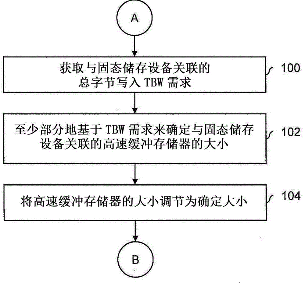
FIG. 1 is a flow diagram illustrating an embodiment of a process to set the size of a cache based at least in part on a Total Bytes Write (TBW) requirement.
FIG. 2 is a diagram illustrating an embodiment of a solid state storage system including a variable size cache.
FIG. 3 is a flow diagram illustrating an embodiment of a process to determine whether a solid state storage system is in a variable size mode or a fixed size mode.
FIG. 4 is a diagram illustrating cache size(s) versus remaining P/E cycles (PEs) in a variable size modeR) A diagram of an embodiment of a graph of (a).
Figure 5 is a flow diagram illustrating an embodiment of a process to determine the size of a cache based at least in part on TBW demand.
FIG. 6 is a flow diagram illustrating an embodiment of a process to determine the size of a cache based at least in part on future states of the solid state storage system during the fixed size mode.
FIG. 7 is a flow diagram illustrating an embodiment of a process to reduce the size of a cache.
FIG. 8 is a flow diagram illustrating an embodiment of a process for writing to a solid state storage device (including cache and conventional drives).
FIG. 9 is a flow diagram illustrating an embodiment of a process for cache upsizing.
Fig. 10 is a flow diagram illustrating an embodiment of a block swapping (block swapping) process to facilitate wear leveling.
Detailed Description
The invention can be implemented in numerous ways, including as a method, an apparatus, a system, a composition of matter, a computer program product embodied on a computer readable storage medium, and/or a processor such as a processor configured to execute instructions stored in and/or provided by a memory coupled to the processor. In this specification, these embodiments, or any other form that the invention may take, may be referred to as techniques. In general, the order of the steps of disclosed processes may be altered within the scope of the invention. Unless otherwise specified, a component (such as a processor or a memory described as being configured to perform a task) may be implemented as a general component that is temporarily configured to perform the task at a given time or as a specific component that is manufactured to perform the task. As used herein, the term "processor" refers to one or more devices, circuits, and/or processing cores configured to process data (such as computer program instructions).
A detailed description of one or more embodiments of the invention is provided below along with accompanying figures that illustrate the principles of the invention. While the invention will be described in conjunction with such embodiments, the invention is not limited to any embodiment. The scope of the invention is limited only by the claims and the invention encompasses numerous alternatives, modifications and equivalents. In the following description, numerous specific details are set forth in order to provide a thorough understanding of the present invention. These details are provided for the purpose of example and the invention may be practiced according to the claims without some or all of these specific details. For the purpose of clarity, technical material that is known in the technical fields related to the invention has not been described in detail so that the invention is not unnecessarily obscured.
FIG. 1 is a flow diagram illustrating an embodiment of a process to set the size of a cache based at least in part on a Total Byte Write (TBW) requirement. For example, the process may be used to set the size of the cache in the solid-state storage medium or drive (e.g., one or more times, if needed) so that response time is improved or optimized without making the cache so large as to violate TBW requirements (e.g., in the future). In some embodiments, the process is performed by a solid state storage device controller that controls how a solid state storage drive or medium is partitioned into a cache portion and a regular drive portion. In some embodiments, the process is performed during a variable size mode or period when the cache is allowed to change size.
At 100, a Total Byte Write (TBW) requirement associated with a solid state storage device is obtained. Unlike other types of storage devices, such as Hard Disk Drives (HDDs), solid state storage devices wear with use. More specifically, program and erase (P/E) cycles break electrical insulation in solid state storage cells, causing them to "leak" with respect to charge as the number of P/E cycles experienced by the solid state storage medium increases. For simplicity, it is sometimes assumed that solid state storage cells wear out when a certain maximum number of P/E cycles is reached. Depending on how solid state storage devices wear out from programming and erasing, system manufacturers often have a Total Byte Write (TBW) requirement that solid state storage media manufacturers must meet.
The TBW requirement is typically related to the amount of write data sent from the host to the solid-state storage device controller. This means that the more write amplification, WA, (e.g., where WA is defined as the ratio of the total number of writes (e.g., host writes plus overhead writes) to the number of host writes for a solid state storage medium or drive), the more robust a solid state storage medium will have to be in order to withstand the additional overhead writes caused by the larger WA value. In one example, a 256GB solid state storage drive has a TBW requirement of 1TB associated with it. If all writes are uniformly spread across the solid-state storage medium, each block (or more generally location) is written about 4 times. However, it is noted that any order or combination of write locations must be supported, so the solid-state storage medium must (also) be able to tolerate write data sent to 1TB of the same logical block address (as an example).
At 102, a size of a cache associated with the solid state storage device is determined based at least in part on the TBW requirement. Some such examples are described in more detail below.
At 104, the cache memory is sized to a determined size. In some embodiments, the size of the cache memory may be adjusted as many times as needed during the variable size mode. In one example, for simpler systems (e.g., consumer products with limited processing power), the size of the cache memory may be set once at the beginning of the variable size mode. For systems where performance is a concern and there are more processing resources available (e.g., enterprise systems), the cache memory may be resized as many times as needed during the variable size mode.
Cache memories typically have a lower bit density than conventional drives. In some examples described below, the cache stores 1 bit per cell, while conventional drivers store 2 bits per cell. Since the total number of blocks (i.e., the number of blocks in the cache plus the number of blocks in a conventional drive) is fixed, increasing the size of the cache reduces the total or overall storage capacity, as the cache typically has fewer bits per block.
The smaller total storage capacity (caused by the increased cache size) means that host writes and overhead writes are more focused, such that each block experiences more programming and erasing. The danger is that if the cache is too large, the TBW requirement will be violated, as an excessively large cache will cause the P/E count to exceed the maximum P/E count (e.g., assuming the block is worn at the maximum P/E count). In other words, there is a tradeoff between the size of the cache and the margin to meet the TBW demand (e.g., measured in terms of excess or remaining P/E cycles before a block wears at the maximum P/E count).
In some embodiments, the process of fig. 1 is used to select the maximum possible size of the cache to improve performance, but not so large as to violate TBW requirements (e.g., because a certain maximum number of P/E cycles is exceeded). That is, the technique enables the size of the cache to be set so that the system has improved performance at the expense of a smaller margin for meeting the TBW demand (e.g., when the TBW demand is met, the cell is close to wearing out, but in reality does not reach some maximum P/E cycle count (assuming for simplicity that the cell fails at some maximum P/E cycle count)).
One benefit of changing the size of the cache (e.g., as opposed to the size of the cache that remains fixed throughout the life of the solid state storage system) is that: the throughput of the system can be increased (where a larger cache size is desirable because it allows for faster response times when there are cache hits) to the extent that TBW requirements allow, without actually violating the TBW requirements.
The following figures illustrate examples of solid state storage systems that perform the processes described in fig. 1.
FIG. 2 is a diagram illustrating an embodiment of a solid state storage system including a variable size cache. The solid-state storage device controller 200 is one example of a system that executes the process of fig. 1. In some embodiments, the solid-state storage device controller 200 is a semiconductor device, such as an Application Specific Integrated Circuit (ASIC) or a Field Programmable Gate Array (FPGA).
In the illustrated example, the solid state storage device 220 is divided into a cache 222 and a conventional drive 224. In this particular example, the cache memory is implemented using Single Level Cells (SLCs) that store 1 bit per cell. The cache 222 is implemented as an SLC so that it can read back faster with fewer errors. Since there are only two distributions (e.g., one is 0 and one is 1), the voltage distributions are located farther away, and thus there are fewer read-back errors and fewer cycles of error correction decoding that need to be performed.
In contrast, the conventional driver 224 is implemented using a multi-level cell (MLC) storing 2 bits per cell. As a result, there are 4 distributions (e.g., one is 00, one is 01, one is 10 and one is 11) and they must squeeze into the same voltage range as the two SLC distributions. The MLC distributions are therefore closer to each other than the SLC distributions, and therefore more readback errors will occur and more error cycles of error correction decoding will need to be performed. This is why the SLC cache 222 can be read back faster with fewer errors than the MLC conventional driver 224. In some embodiments, the conventional driver 224 is implemented using a Three Level Cell (TLC) that stores 3 bits per cell.
The host interface 204 receives a read command and a write command from a host (not shown). Internal to the host interface 204 is a write byte counter 202 that counts the amount of write data received from the host. In some embodiments, TBW is obtained from write byte counter 202PThe value of (t) (the amount of host data that has been written and counted for TBW demand).
In this example, the cache controller 206 periodically determines the size of the cache 222 and is one example of a component that performs step 102 in FIG. 1. In some embodiments, the logical-to-physical (L2P) mapping table 208 is used to record which portion of the solid state storage device 220 belongs to the cache 222 and which portion of the solid state storage device 220 belongs to the regular drive 224. For example, the L2P mapping table 208 may include ranges of (e.g., physical) addresses in the cache 222 and the regular drive 224.
In some embodiments, the solid state storage 220 is configured to support a cache memory, the size of which is configurable or otherwise adjustable. In some such embodiments, the solid state storage device 220 may expose an interface or control to the solid state storage device controller 220 to specify bit densities for the cache memory 222 and the regular drive 224 (e.g., SLC, MLC, tertiary cell (TLC), etc.), and which (e.g., physical) addresses are in the cache memory and which (e.g., physical) addresses are in the regular drive.
In one example of how the cache memory 222 and the regular drive 224 are used, a host (not shown) is aware that a cache memory is present and has the ability to mark, tag, or otherwise indicate (if needed) what host write data should be stored in the cache memory 222 and what host write data should be stored in the regular drive 224. For example, if a host write received by the host interface 204 includes a cache tag, the write data is stored in the cache 222. If not, the write data is stored in the regular drive 224.
Alternatively, the host is unaware of the cache and/or does not have control over what host write data is stored in the cache. In one example of such a system, the temperature identifier 212 determines the temperature of the write data received from the host. Data is hot if it will be invalidated (or at least considered invalid) or otherwise overwritten shortly in the future. If the data remains valid (i.e., not overwritten) for a long period of time, the data is cold. Host write temperature identifier 212 may use any suitable technique to determine the temperature of write data received from the host. Based on the temperature determined by the temperature identifier 212, hot data is stored in the cache memory 222 and cold data is stored in the regular drive 224. These examples of how data is allocated to cache memory 222 and conventional drivers 224 are illustrative only and not intended to be limiting.
As will be described in more detail below, to resize the cache 222 (see step 104 in fig. 1), a garbage collector 210 may be used in some embodiments. Alternatively, enough free blocks (i.e., blocks that are empty and available to be written to) may already exist (e.g., garbage collected is not performed) in the cache 222 or the regular driver 224 to be reassigned to another block, and resizing is a relatively simple process (e.g., the cache controller 206 updates the information stored in the logical-to-physical mapping table 208 so that empty blocks (empty blocks) are moved from the cache 222 to the regular driver 224, or vice versa).
In some embodiments, the solid state storage 220 includes some extra capacity (e.g., non-asserted) referred to as headroom (over provisioning). For example, a (purportedly) 1GB drive with 7% headroom actually has 1.07GB of real storage space.
In some embodiments, the solid-state storage system begins in a variable-size mode (e.g., the size of the cache 222 is allowed to change in the variable-size mode) and ends in a fixed-size mode (e.g., the size of the cache 222 is fixed in the fixed-size mode). The following figures illustrate one such example.
FIG. 3 is a flow diagram illustrating an embodiment of a process to determine whether a solid state storage system is in a variable size mode or a fixed size mode. In some embodiments, the process is performed by a solid state storage device controller.
At 300, it is determined whether one or more fixed size mode criteria have been met. For example, assume that there is a certain value PER,PERIs the number of P/E cycles that can be experienced by the solid-state storage medium during the variable-size mode before switching to the fixed-size mode. For example, all program and erase operations to a solid-state storage medium (e.g., cache or regular drive) will be to the PERThe value is counted. If the P/E count (e.g., for the entire solid-state storage medium or drive as a whole) satisfies PERValue, then the exemplary fixed size mode criteria will be met.
As will be described in more detail below, changing the size of the cache (e.g., from a first/starting cache size to a second cache size during a variable size mode) sometimes corresponds to changing the PERValue (e.g., from a first/starting PERValue to the second PERValue). Thus, in some embodiments, the decision or test at step 300 includes determining a PERWhether the count is associated with the current or latest PERThe values match.
If the fixed size mode criteria are met, then the fixed size is obtained at step 302. For example, there may be some predefined size to which the cache should be set. In some embodiments, the size calculation at step 102 of FIG. 1 assumes a particular size of the cache during the fixed size mode, and the size used in the calculation is retrieved at step 302.
At 304, the cache is resized to a fixed size. In some embodiments, garbage collection is used to resize cache and regular drivers. In some embodiments, there are enough free blocks in the cache and conventional drivers so that the process of resizing is relatively simple.
The process then ends because the cache size is not allowed to be subsequently changed once the cache is in the fixed size mode.
If the fixed size mode criteria are not met at step 300, the process of FIG. 1 is performed because the system is (still) in the variable size mode. It is noted that it may not be desirable to continually recalculate the cache size and continually adjust it, so the process of FIG. 1 may not begin immediately after the process exits step 300 via the NO path.
After the process of fig. 1 ends, it is determined (again) at step 300 whether the fixed size mode criteria are met. That is, although the system starts in the variable size mode and is allowed to go from the variable size mode to the fixed size mode, the system is not allowed to go from the fixed size mode to the variable size mode.
The following figures describe more specific examples of how the size of the cache memory is determined at step 102 of FIG. 1. First, a detailed example is discussed. Then, some generalizations regarding detailed examples are discussed.
TBWR(t) is the amount of data (e.g., in MB, TB, etc.) that remains written (e.g., to satisfy the TBW requirement) at time t. For example, subscript R indicates the remainder. TBWR(t) can be written as:

wherein:

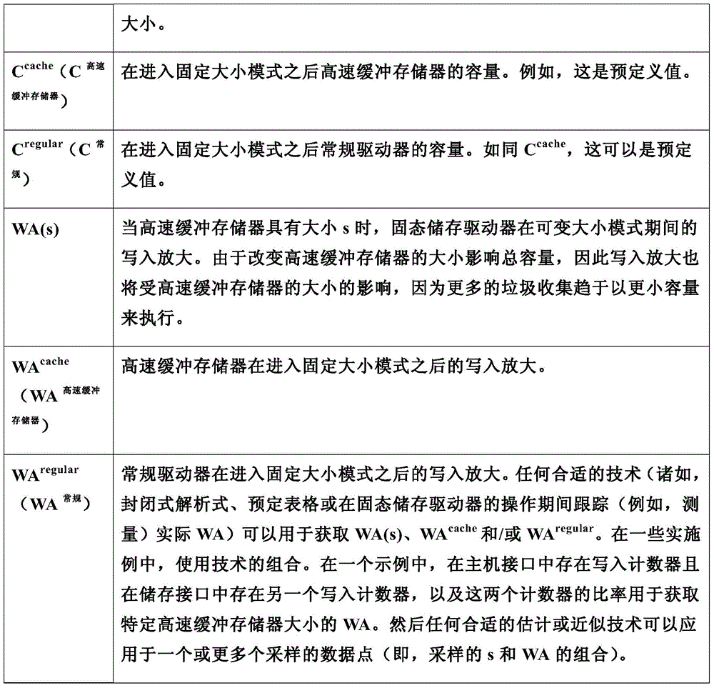
table 1: input in equation (1)
Some of the inputs in equation (1), such as c (t) and wa(s), vary with s (i.e., the size of the cache memory). As described above, c (t) depends on s, since cache and conventional drivers typically have different bit densities (e.g., SLC and MLC), the total capacity will depend on the size of the cache. Similarly, if the capacity varies with s, the write amplification also varies with s. For example, assume that the size of the cache memory increases such that the capacity of the solid-state storage drive (as a whole) decreases. This will tend to cause more garbage collection and will in turn cause more write amplification.
Some of the inputs in equation (1) (such as PE)cacheAnd PEregular) Following PERBut may vary. Since the size of the cache and the conventional driver during the fixed-size mode is predefined, the number of P/E cycles that need to be supported by the cache and the conventional driver depends on how many P/E cycles (i.e., PE's) will be processed or otherwise experienced during the variable-size modeR) So that they do not need to be processed later during the fixed size mode.
Remaining inputs Ccache、Cregular、WAcacheAnd WAregularNeither s nor PER。
TBWR(t) can be written as follows, where the inequality is derived from the TBW requirement:
TBWR(t)≥TBW(t)-TBWP(t) (2)
wherein, TBWp(t) is the amount of data (e.g., in units of MB, TB, etc.) that has been written at time t (e.g., and its count of TBW demand). For example, subscript P may represent past or previous. In one example, there is a counter in the host interface (e.g., in the solid-state storage device controller) that counts the number of transfers from the host to the solid-state storage device controllerWrite data amount, and acquire TBW from such counterp(t)。
The input in equation (1) depends on s, PEROr independent of s and PERMeaning that s and PE are presentRThat does not violate equation (2). In other words, the size of the cache memory may be adjusted as many times as needed during the variable size mode, with s and PE each carefully selectedRSo that equation (2) remains. For example, during the initialization size at time 0, the size of the cache is set to s0And PERIs set as PER,0Wherein(s)0,PER,0) Equation (2) is not violated. At time t1At a later point in time (still during the variable size mode), the size of the cache may be set to s1And PERIs set as PER,1Wherein(s)1,PER,1) Equation (2) is not violated. Suppose that the drive has experienced PE (as a whole) due to solid state storageROne P/E cycle, thus satisfying the current PERValue (current PE at this point in time)RValue is PER,1). The system is then switched to a fixed size mode, for example by setting the size of the cache memory to some predefined size and the size of the regular drive to another predefined size.
The following figures show (s, PE) obtained using equation (1)R) Does not cause equation (2) to be violated.
FIG. 4 is a diagram of an embodiment illustrating a graph of cache size(s) versus remaining P/E cycles in a variable size mode. In the illustrated example, the x-axis of diagram 400 is the cache size(s), while the y-axis of diagram 400 is the remaining P/E cycles (PE) in the variable size modeR)。
Shaded region 402 shows (s, PE) that does not violate TBW requirements (e.g., as represented in equation (2))R) Combinations of (a) and (b). As long as a data point is selected in the shadow 402, calculating the selected cache size does not violate TBW requirements. For example, if data point A (410),B (412), C (414), or D (416) is selected, then the corresponding combination of cache size and remaining P/E cycles (i.e.,(s)A,PER,A)、(SB,PER,B)、(SC、 PER,C) And (S)D,PER,D) Will not violate TBW requirements. In contrast, point E (418), which is outside of the shaded region 402, corresponds to (S)E,PER,E) Data point of (S)E,PER,E) Is a combination that violates the TBW requirement.
For example, assume that point B (412) is selected. The cache will be set to SBOf (2), and PER,BWill be used to determine when to switch from the variable size mode to the fixed size mode.
In some embodiments, the cache size associated with point C (414) is selected because it optimizes throughput by selecting the largest cache size (which does not violate TBW requirements). This may be desirable, for example, in applications where response time is a high priority. In some embodiments, the cache size associated with point B (412) is selected because it is a more balanced trade-off between performance and margin amount (the amount by which TBW demand meets the margin). In some embodiments, the cache size associated with point A (410) is selected. This may be desirable in applications where response time is not a concern but rather has a large margin to meet TBW requirements.
Note that the cache memory may be resized as many times as necessary during the variable size mode, if desired. Each time the process of FIG. 1 is performed, (s, PE) showing no violations of TBW requirements can be redrawn or recalculatedR) A new graph of combinations of (a). For example, updated or more current information may affect the input of equation (1), which in turn affects (s, PE) that does not violate TBW requirementsR) Combinations of (a) and (b).
In the context of fig. 1, step 102 may be performed in the following manner in accordance with the example shown in the figure.
Figure 5 is a flow diagram illustrating an embodiment of a process to determine the size of a cache based at least in part on TBW demand. In some embodiments, step 102 in FIG. 1 comprises the process of FIG. 5.
At 500, a plurality of combinations of (1) cache size and (2) remaining program and erase (P/E) counts in the variable size mode are determined that do not violate TBW requirements. For example, in FIG. 4, the shaded area (402) shows (s, PE) that does not violate TBW requirementsR) Combinations of (a) and (b).
At 502, one of a plurality of combinations is selected, wherein a cache size corresponding to the selected combination is the determined cache size and a remaining P/E count corresponding to the selected combination is associated with an end of the variable size mode. Any suitable selection technique may be employed (some examples of which are described above).
Returning to equation (1), the determination of the cache size is performed during the variable size mode, but consider what state the solid state storage device will be in during the later fixed size mode. The following figures illustrate such examples.
FIG. 6 is a flow diagram illustrating an embodiment of a process to determine the size of a cache based at least in part on future states of the solid state storage system during the fixed size mode. In some embodiments, step 102 in FIG. 1 comprises the process of FIG. 6.
At 600, a plurality of combinations of (1) cache size and (2) remaining program and erase (P/E) counts in the variable size mode that do not violate TBW requirements are determined, wherein the determination is based at least in part on a future state of the solid state storage device during the fixed size mode following the variable size mode. For example, the future state may include one or more of the following: PE (polyethylene)cache、PEregular、Ccache、Cregular、WAcacheOr WAregular(see Table 1).
At 602, one of a plurality of combinations is selected, wherein a cache size corresponding to the selected combination is the determined cache size and a remaining P/E count corresponding to the selected combination is associated with an end of the variable size mode. Some examples are described above.
Returning to FIG. 1, step 104 is associated with resizing the cache (and, correspondingly, the size of the conventional drive) to a determined size. The following figures describe one such example.
FIG. 7 is a flow diagram illustrating an embodiment of a process to reduce the size of a cache. For example, step 104 in FIG. 1 may include the process of FIG. 7 when the size of the cache needs to be reduced. Note that the process of fig. 7 correspondingly causes the size of the conventional drive to increase.
At 700, it is determined whether to reduce the cache size. If the cache size does not need to be reduced, the process ends. (Note that in some cases, step 816 of FIG. 8 is performed next after the process of FIG. 7 ends). this check explicitly illustrates that FIG. 7 relates to shrinking the size of the cache (e.g., and not expanding the size of the cache).
If it is determined at 700 that a reduction in cache size is not required, then at 702 it is determined whether a size reassignment flag has been set. The size reassignment flag is used to ensure that at most one resizing operation runs immediately. If the size reassignment flag has been set at 702, the process will continue with the check at step 702 until the flag is cleared.
If (or once) the size reallocation flag is cleared at step 702, the size reallocation flag is set at step 704 (e.g., so that another resizing process cannot run while the resizing process is running). One or more empty cache blocks are then designated as empty regular drive blocks at 706. According to embodiments, the change may be recorded in various ways (e.g., by changing an (e.g., physical) address corresponding to the cache/regular drive and stored in a logical-to-physical mapping table, or notifying the solid state storage drive itself of the change if the solid state storage drive is configured to manage and/or record what portions of itself correspond to the cache and what portions of itself correspond to the regular drive).
In this particular example, it is assumed that the system maintains a minimum number of free blocks in the cache memory so that one or more free blocks can be transferred to the regular drive. As such, in this example, there is no need to perform garbage collection or otherwise free the cache block prior to the designation at 706. However, after the specification of step 706, garbage collection may need to be performed in order to increase the empty cache blocks so that the minimum is met.
For the case when the regular drive is full, it is advantageous to always ensure that there is at least a minimum number of empty cache blocks (e.g., the LBA range utilized is equal to the user capacity). If a minimum number of empty cache blocks are not maintained, the cache typically frees the blocks by garbage collecting data from the cache into the regular drive. However, this would not be possible when the conventional drive is full, since there is no place to place valid data from the cache. As such, when this situation occurs, it may be desirable to always maintain some minimum number of empty cache blocks. Another advantage is that the downsizing can be done fairly quickly (e.g., without waiting for garbage collection, in some systems only allowing garbage collection to occur at a particular time and/or after a particular number of host accesses have been performed).
The following figures illustrate exemplary larger contexts in which the cache downsizing process of FIG. 7 may be performed.
FIG. 8 is a flow diagram illustrating an embodiment of a process for writing to a solid state storage device (including cache and conventional drives). In the illustrated example, the process illustrates an example of how or when the cache downsizing process is incorporated into the large context of the operation of the solid state storage system. The process may be performed by a solid-state storage device controller (such as controller 200 in fig. 2).
At 800, host data is written to a cache. In this example, new write data is always written to the cache even if its final destination is a regular drive. In some cases, for example, if the data is classified as hot or the host has indicated that the write data should be stored in the cache, the data may remain there. Alternatively, if the data is classified as cold data or the host indicates that it should be stored in a regular drive, the data may be transferred to the regular drive. For example, data can be written to the cache faster than with conventional drives, so to speed up write time, data is first written to the cache and then copied (if needed) from the cache to the conventional drive.
At 802, a determination is made as to whether an open cache block is full of host data. For example, when writing host data to the cache, the currently open block in the cache may become full and a new block in the cache to which the host data is directed and written needs to be opened. If the open cache block is not full at 802, the process returns to writing host data at step 800. For example, an open cache block may not be completely full, so a new block need not be opened.
If it is determined at step 802 that the open cache block is full, then at step 804 it is determined whether a minimum number of empty cache blocks are available. Similar to the example above, a minimum number of empty cache blocks is maintained in the cache. If a minimum number of empty cache blocks are available at step 804, the cache blocks are opened at 806 and more host data is written at step 800.
If at step 804 the minimum number of empty cache blocks are not available, then at 808 garbage collection is performed on the cache, wherein valid data in the ingested cache block is output to the regular driver. This causes the block to be free in the cache.
At 810, it is determined whether garbage collection has achieved a minimum number of empty cache blocks. If so, the size reassignment flag is reset 812 and the process ends. Note that clearing the flag at step 812 enables another cache resizing process to be operated (see, e.g., the description of the check at step 702 in FIG. 7).
If the minimum number of empty cache blocks is not achieved by garbage collection at step 810, then a determination is made at 814 as to whether the open regular drive blocks are full according to garbage collection. If so, the process of FIG. 7 is performed (i.e., the cache memory is reduced in size, which results in free blocks being added to the regular drive).
After the process of FIG. 7 is performed, at step 816, the regular driver blocks are opened for garbage collection processes that use empty regular driver blocks (which come from the process of cache scaling down). After opening the regular drive blocks at step 816 or if it is decided at step 814 not to open the regular drive blocks, garbage collection is performed again at step 808.
The process shown in fig. 8 is a relatively detailed example. More generally, the process of FIG. 7 may be performed before opening the regular drive block at step 816, and then performing garbage collection at step 808. One advantage of merging the cache downsizing process into the garbage collection process is that the cache garbage collection process already exists and has time to be optimized. That is, there is already a process of reducing the size of the cache (and the process has time to be refined), so no "unnecessary duplication of labor" is required. A second advantage is that garbage collection of the cache must occur, so concurrent cache downsizing operations do not introduce new overhead operations.
Naturally, the size of the cache memory may be increased in some cases. The following is an example of such a process.
FIG. 9 is a flow diagram illustrating an embodiment of a process for cache upsizing. In some embodiments, step 104 in FIG. 1 comprises the process of FIG. 9. At 900, it is determined whether to increase the cache size. If so, at 902, it is determined whether a minimum number of empty regular drive blocks are available. As in the above example, the system ensures that there is at least some minimum number of empty blocks in a regular drive (like a cache).
If a minimum number of empty regular drive blocks are available at 902, one or more empty regular drive blocks are designated as empty cache blocks at 908. If a minimum number of empty regular drive blocks are not available at 902, the system idles some blocks by scheduling garbage collection of regular drives. In this example, garbage collection waits until some predefined time or predefined event in order to reduce overhead writes (e.g., as measured by write amplification).
Step 906 checks to see if garbage collection has been completed. The process will wait at step 906 until garbage collection has been completed. Once garbage collection has completed at step 906, or if a minimum number of empty regular drive blocks are available at step 902, one or more empty regular drive blocks are designated as empty cache blocks at 908.
Wear leveling (wear leveling) is a process by which blocks with lower P/E counts are freed so that new free blocks are hopefully able to be written, resulting in more equal P/E counts for solid-state storage devices. Wear leveling is performed not only in the cache and the regular drive, but also between the cache and the regular drive, so that all blocks wear out at the same time (e.g., independent of whether they are in the cache or the regular drive). The following figures illustrate an exemplary block swapping process that may facilitate wear leveling. In some embodiments, the following process is performed in conjunction with FIG. 1.
FIG. 10 is a flow diagram illustrating an embodiment of a block exchange process to facilitate wear leveling. In the illustrated example, garbage collection and wear leveling is performed independently for the cache and the regular driver (e.g., where the garbage collection and/or wear leveling process uses a different selection technique for source blocks and/or destination blocks in the cache and regular driver), and may be performed each time wear leveling or garbage collection is performed for the cache or regular driver. In this example, it is assumed that each of the cache and regular drives have their own pool of empty or free blocks. There is no common pool of empty blocks (at least in this example) shared by, for example, both the cache and the regular drives.
At 1000, it is determined whether the cache has a higher average P/E count than a conventional drive. If so, at 1002, the free cache block with the highest P/E count is swapped with the free regular drive block with the lowest P/E count. On the other hand, if the regular drive has a higher P/E count, then at 1004 the free cache block with the lowest P/E count is swapped with the free regular drive block with the highest P/E count.
One advantage of the above process is that it takes into account current system conditions such that portions of the storage device (i.e., cache or regular drive) that become more worn get blocks with low (lower) P/E counts from other portions of the drive. Another advantage is that it does not require (extra) data writes, so it has low overhead and does not affect WA.
Note that the above process is a passive process and more active or aggressive techniques may be performed in which additional garbage collection operations and/or new garbage collection operations and/or wear leveling operations are actively triggered to idle blocks and then swap blocks. For example, the process shown in FIG. 10 takes no action and waits for blocks to be freed using existing or current garbage collection operations and/or wear leveling operations. Naturally, more aggressive or aggressive switching techniques will make an adverse contribution to the WA.
Although the foregoing embodiments have been described in some detail for purposes of clarity of understanding, the invention is not limited to the details provided. There are many alternative ways of implementing the invention. The disclosed embodiments are illustrative and not restrictive.
As can be seen from the above embodiments, the present invention provides the following technical solutions.
a solid state storage device; and
a solid state storage device controller configured to:
acquiring a total byte write TBW requirement associated with the solid-state storage device;
determining a size of a cache associated with the solid state storage based at least in part on the TBW requirement; and
the cache memory is sized to a certain size.
Solution 3. the system of solution 1, wherein the cache memory comprises a plurality of single level cells SLC and the conventional drive portion of the solid state storage device comprises one or more of: multiple multi-level cells MLC or multiple three-level cells TLC.
Technical solution 4. the system of technical solution 1, wherein the solid-state storage device controller is further configured to:
determining whether one or more fixed size mode criteria have been met;
if the fixed size mode criteria have been met:
obtaining a fixed size; and
resizing the cache to a fixed size; and
if the fixed size mode criteria are not met, the steps of acquiring, determining and adjusting are performed.
Technical solution 5 the system of claim 1, wherein the solid-state storage device controller is configured to determine a size of the cache memory, comprising:
determining a plurality of combinations of (1) cache size and (2) remaining program and erase P/E counts in the variable size mode that do not violate TBW requirements; and
one of the plurality of combinations is selected, wherein the cache size corresponding to the selected combination is the determined cache size and the remaining P/E count corresponding to the selected combination is associated with the end of the variable size mode.
Solution 6. the system of solution 5, wherein determining the plurality of combinations is based at least in part on a future state of the solid state storage device during a fixed size mode subsequent to the variable size mode.
The system according to claim 1, wherein:
the size of the cache memory is reduced; and
the solid-state storage device controller is configured to reduce a size of the cache memory, including:
judging whether a size redistribution flag is set; and
if it is determined that the size reassignment flag is not set:
setting a size redistribution flag; and
one or more empty cache blocks are designated as empty regular drive blocks.
Technical solution 8 the system of claim 7, wherein the solid-state storage device controller is further configured to:
performing a garbage collection process on the cache memory, wherein valid data in the ingested cache memory block is output to the regular driver; and
the regular driver blocks are opened for garbage collection processes that use empty regular driver blocks from the process of cache memory downsizing.
Solution 9. the system of solution 1, wherein the solid-state storage device controller is further configured to:
determining whether the cache memory has a higher average program and erase P/E count than a conventional drive;
swapping one or more free cache blocks having the highest P/E count with one or more free regular driver blocks having the lowest P/E count if it is determined that the cache has a higher average P/E count; and
if it is determined that the regular drives have a higher average P/E count, the one or more free cache blocks having the lowest P/E count are swapped with the one or more free regular drive blocks having the highest P/E count.
The method of claim 10, comprising:
acquiring a total byte write TBW requirement associated with the solid-state storage device;
determining a size of a cache associated with the solid state storage based at least in part on the TBW requirement; and
the cache memory is sized to a certain size.
Solution 11 the method of solution 10 wherein the method is performed by a semiconductor device comprising one or more of the following: an application specific integrated circuit ASIC or a field programmable gate array FPGA.
Solution 12. the method of solution 10, wherein the cache memory comprises a plurality of single level cells SLC and the conventional driver portion of the solid state storage device comprises one or more of: multiple multi-level cells MLC or multiple three-level cells TLC.
The method according to claim 10, further comprising:
determining whether one or more fixed size mode criteria have been met;
if the fixed size mode criteria have been met:
obtaining a fixed size; and
resizing the cache to a fixed size; and
if the fixed size mode criteria are not met, the steps of acquiring, determining and adjusting are performed.
The method of claim 14, wherein the determining the size of the cache memory comprises:
determining a plurality of combinations of (1) cache size and (2) remaining program and erase P/E counts in the variable size mode that do not violate TBW requirements; and
one of the plurality of combinations is selected, wherein the cache size corresponding to the selected combination is the determined cache size and the remaining P/E count corresponding to the selected combination is associated with the end of the variable size mode.
Claim 15 the method of claim 14, wherein determining the plurality of combinations is based at least in part on a future state of the solid state storage device during a fixed size mode subsequent to the variable size mode.
The method of claim 10, wherein:
the size of the cache memory is reduced; and
reducing the size of a cache memory, comprising:
judging whether a size redistribution flag is set; and
if it is determined that the size reassignment flag is not set:
setting a size redistribution flag; and
one or more empty cache blocks are designated as empty regular drive blocks.
The method according to claim 16, further comprising:
performing a garbage collection process on the cache memory, wherein valid data in the ingested cache memory block is output to the regular driver; and
the regular driver blocks are opened for garbage collection processes that use empty regular driver blocks from the process of cache memory downsizing.
The method according to claim 10, further comprising:
determining whether the cache memory has a higher average program and erase P/E count than a conventional drive;
swapping one or more free cache blocks having the highest P/E count with one or more free regular driver blocks having the lowest P/E count if it is determined that the cache has a higher average P/E count; and
if it is determined that the regular drives have a higher average P/E count, the one or more free cache blocks having the lowest P/E count are swapped with the one or more free regular drive blocks having the highest P/E count.
A computer program product, the computer program product being embodied as a non-transitory computer readable storage medium and comprising computer instructions for:
acquiring a total byte write TBW requirement associated with the solid-state storage device;
determining a size of a cache associated with the solid state storage based at least in part on the TBW requirement; and
the cache memory is sized to a certain size.
Claim 20 the computer program product of claim 19, wherein determining the size of the cache memory comprises:
determining a plurality of combinations of (1) cache size and (2) remaining program and erase P/E counts in the variable size mode that do not violate TBW requirements; and
one of the plurality of combinations is selected, wherein the cache size corresponding to the selected combination is the determined cache size and the remaining P/E count corresponding to the selected combination is associated with the end of the variable size mode.
Claims (20)
1. A solid state storage system, comprising:
a solid-state storage device including a cache and configured to operate in a variable size mode in which a size of the cache is allowed to change and a fixed size mode in which the size of the cache is fixed; and
a solid state storage device controller configured to:
acquiring a total byte write requirement associated with the solid-state storage device;
determining a size of a cache based at least in part on a total byte write requirement and remaining program and erase P/E counts;
resizing the cache to a certain size when the program and erase P/E counts are less than a maximum count; and
when the remaining program and erase P/E counts are greater than or equal to the maximum count, the cache memory transitions to a fixed size mode, adjusting the size of the cache memory to a fixed size.
2. The solid state storage system of claim 1, wherein the solid state storage device controller comprises a semiconductor device comprising one or more of: an application specific integrated circuit ASIC or a field programmable gate array FPGA.
3. The solid state storage system of claim 1, wherein the cache memory comprises a plurality of Single Level Cells (SLCs) and the regular drive portion of the solid state storage device comprises one or more of: multiple multi-level cells MLC or multiple three-level cells TLC.
4. The solid-state storage system of claim 1, wherein the solid-state storage device controller is further configured to:
determining whether one or more fixed size mode criteria have been met;
if the fixed size mode criteria have been met:
obtaining a fixed size; and
resizing the cache to a fixed size; and
if the fixed size mode criteria are not met, the steps of acquiring, determining and adjusting are performed.
5. The solid-state storage system of claim 1, wherein the solid-state storage device controller is configured to determine a size of the cache memory, comprising:
determining a plurality of combinations of (1) cache size and (2) remaining program and erase P/E counts in a variable size mode, the plurality of combinations not violating total byte write requirements; and
one of the plurality of combinations is selected, wherein the cache size corresponding to the selected combination is the determined cache size and the remaining P/E count corresponding to the selected combination is associated with the end of the variable size mode.
6. The solid state storage system of claim 5, wherein determining the plurality of combinations is based at least in part on a future state of the solid state storage device during a fixed size mode subsequent to a variable size mode.
7. The solid state storage system of claim 1, wherein:
the size of the cache memory is reduced; and
the solid-state storage device controller is configured to reduce a size of the cache memory, including:
judging whether a size redistribution flag is set; and
if it is determined that the size reassignment flag is not set:
setting a size redistribution flag; and
one or more empty cache blocks are designated as empty regular drive blocks.
8. The solid-state storage system of claim 7, wherein the solid-state storage device controller is further configured to:
performing a garbage collection process on the cache memory, wherein valid data in the ingested cache memory block is output to the regular driver; and
the regular driver blocks are opened for garbage collection processes that use empty regular driver blocks from the process of cache memory downsizing.
9. The solid-state storage system of claim 1, wherein the solid-state storage device controller is further configured to:
determining whether the cache memory has a higher average program and erase P/E count than a conventional drive;
swapping one or more free cache blocks having the highest P/E count with one or more free regular driver blocks having the lowest P/E count if it is determined that the cache has a higher average P/E count; and
if it is determined that the regular drives have a higher average P/E count, the one or more free cache blocks having the lowest P/E count are swapped with the one or more free regular drive blocks having the highest P/E count.
10. A method of setting a size of a cache memory, comprising:
obtaining a total byte write demand associated with a solid state storage device that includes a cache and is configured to operate in a variable size mode in which a size of the cache is allowed to change and a fixed size mode in which the size of the cache is fixed;
determining a size of a cache based at least in part on a total byte write requirement and remaining program and erase P/E counts;
resizing the cache to a certain size when the program and erase P/E counts are less than a maximum count, and
when the remaining program and erase P/E counts are greater than or equal to the maximum count, the cache memory transitions to a fixed size mode, adjusting the size of the cache memory to a fixed size.
11. The method of claim 10, wherein the method is performed by a semiconductor device comprising one or more of: an application specific integrated circuit ASIC or a field programmable gate array FPGA.
12. The method of claim 10, wherein the cache memory comprises a plurality of Single Level Cells (SLCs) and the regular driver portion of the solid state storage device comprises one or more of: multiple multi-level cells MLC or multiple three-level cells TLC.
13. The method of claim 10, further comprising:
determining whether one or more fixed size mode criteria have been met;
if the fixed size mode criteria have been met:
obtaining a fixed size; and
resizing the cache to a fixed size; and
if the fixed size mode criteria are not met, the steps of acquiring, determining and adjusting are performed.
14. The method of claim 10, wherein determining the size of the cache memory comprises:
determining a plurality of combinations of (1) cache size and (2) remaining program and erase P/E counts in a variable size mode, the plurality of combinations not violating total byte write requirements; and
one of the plurality of combinations is selected, wherein the cache size corresponding to the selected combination is the determined cache size and the remaining P/E count corresponding to the selected combination is associated with the end of the variable size mode.
15. The method of claim 14, wherein determining the plurality of combinations is based at least in part on a future state of the solid state storage device during a fixed size mode subsequent to a variable size mode.
16. The method of claim 10, wherein:
the size of the cache memory is reduced; and
reducing the size of a cache memory, comprising:
judging whether a size redistribution flag is set; and
if it is determined that the size reassignment flag is not set:
setting a size redistribution flag; and
one or more empty cache blocks are designated as empty regular drive blocks.
17. The method of claim 16 further comprising:
performing a garbage collection process on the cache memory, wherein valid data in the ingested cache memory block is output to the regular driver; and
the regular driver blocks are opened for garbage collection processes that use empty regular driver blocks from the process of cache memory downsizing.
18. The method of claim 10 further comprising:
determining whether the cache memory has a higher average program and erase P/E count than a conventional drive;
swapping one or more free cache blocks having the highest P/E count with one or more free regular driver blocks having the lowest P/E count if it is determined that the cache has a higher average P/E count; and
if it is determined that the regular drives have a higher average P/E count, the one or more free cache blocks having the lowest P/E count are swapped with the one or more free regular drive blocks having the highest P/E count.
19. A non-transitory computer readable storage medium having stored thereon computer instructions which, when executed by a processor, implement the steps of:
obtaining a total byte write demand associated with a solid state storage device that includes a cache and is configured to operate in a variable size mode in which a size of the cache is allowed to change and a fixed size mode in which the size of the cache is fixed;
determining a size of a cache based at least in part on a total byte write requirement and remaining program and erase P/E counts;
resizing the cache to a certain size when the program and erase P/E counts are less than a maximum count, and
when the remaining program and erase P/E counts are greater than or equal to the maximum count, the cache memory transitions to a fixed size mode, adjusting the size of the cache memory to a fixed size.
20. The non-transitory computer readable storage medium of claim 19, wherein the step of determining the size of the cache memory comprises:
determining a plurality of combinations of (1) cache size and (2) remaining program and erase P/E counts in a variable size mode, the plurality of combinations not violating total byte write requirements; and
one of the plurality of combinations is selected, wherein the cache size corresponding to the selected combination is the determined cache size and the remaining P/E count corresponding to the selected combination is associated with the end of the variable size mode.
Applications Claiming Priority (4)
| Application Number | Priority Date | Filing Date | Title |
|---|---|---|---|
| US201462060387P | 2014-10-06 | 2014-10-06 | |
| US62/060,387 | 2014-10-06 | ||
| US14/843,632 | 2015-09-02 | ||
| US14/843,632 US10127157B2 (en) | 2014-10-06 | 2015-09-02 | Sizing a cache while taking into account a total bytes written requirement |
Publications (2)
| Publication Number | Publication Date |
|---|---|
| CN105487986A CN105487986A (en) | 2016-04-13 |
| CN105487986B true CN105487986B (en) | 2021-05-07 |
Family
ID=55632911
Family Applications (1)
| Application Number | Title | Priority Date | Filing Date |
|---|---|---|---|
| CN201510642769.8A Active CN105487986B (en) | 2014-10-06 | 2015-09-30 | Sizing a cache memory to account for total byte write requirements |
Country Status (2)
| Country | Link |
|---|---|
| US (1) | US10127157B2 (en) |
| CN (1) | CN105487986B (en) |
Families Citing this family (54)
| Publication number | Priority date | Publication date | Assignee | Title |
|---|---|---|---|---|
| US10042565B2 (en) * | 2014-10-16 | 2018-08-07 | Futurewei Technologies, Inc. | All-flash-array primary storage and caching appliances implementing triple-level cell (TLC)-NAND semiconductor microchips |
| US20160225459A1 (en) * | 2015-01-30 | 2016-08-04 | Micron Technology, Inc. | Apparatuses operable in multiple power modes and methods of operating the same |
| US9697134B2 (en) | 2015-06-10 | 2017-07-04 | Micron Technology, Inc. | Memory having a static cache and a dynamic cache |
| US10359933B2 (en) * | 2016-09-19 | 2019-07-23 | Micron Technology, Inc. | Memory devices and electronic systems having a hybrid cache including static and dynamic caches with single and multiple bits per cell, and related methods |
| CN108121663B (en) * | 2016-11-29 | 2022-05-03 | 群联电子股份有限公司 | Data storage method, memory storage device and memory control circuit unit |
| US10325668B2 (en) * | 2017-04-05 | 2019-06-18 | Micron Technology, Inc. | Operation of mixed mode blocks |
| US10877898B2 (en) | 2017-11-16 | 2020-12-29 | Alibaba Group Holding Limited | Method and system for enhancing flash translation layer mapping flexibility for performance and lifespan improvements |
| US10496548B2 (en) | 2018-02-07 | 2019-12-03 | Alibaba Group Holding Limited | Method and system for user-space storage I/O stack with user-space flash translation layer |
| US11379155B2 (en) | 2018-05-24 | 2022-07-05 | Alibaba Group Holding Limited | System and method for flash storage management using multiple open page stripes |
| WO2020000136A1 (en) | 2018-06-25 | 2020-01-02 | Alibaba Group Holding Limited | System and method for managing resources of a storage device and quantifying the cost of i/o requests |
| US10921992B2 (en) | 2018-06-25 | 2021-02-16 | Alibaba Group Holding Limited | Method and system for data placement in a hard disk drive based on access frequency for improved IOPS and utilization efficiency |
| US10996886B2 (en) | 2018-08-02 | 2021-05-04 | Alibaba Group Holding Limited | Method and system for facilitating atomicity and latency assurance on variable sized I/O |
| US11327929B2 (en) | 2018-09-17 | 2022-05-10 | Alibaba Group Holding Limited | Method and system for reduced data movement compression using in-storage computing and a customized file system |
| KR102516246B1 (en) * | 2018-10-29 | 2023-03-30 | 마이크론 테크놀로지, 인크. | SLC cache allocation |
| US10977122B2 (en) | 2018-12-31 | 2021-04-13 | Alibaba Group Holding Limited | System and method for facilitating differentiated error correction in high-density flash devices |
| US11061735B2 (en) | 2019-01-02 | 2021-07-13 | Alibaba Group Holding Limited | System and method for offloading computation to storage nodes in distributed system |
| US11132291B2 (en) | 2019-01-04 | 2021-09-28 | Alibaba Group Holding Limited | System and method of FPGA-executed flash translation layer in multiple solid state drives |
| US11200337B2 (en) | 2019-02-11 | 2021-12-14 | Alibaba Group Holding Limited | System and method for user data isolation |
| US10970212B2 (en) | 2019-02-15 | 2021-04-06 | Alibaba Group Holding Limited | Method and system for facilitating a distributed storage system with a total cost of ownership reduction for multiple available zones |
| US11061834B2 (en) | 2019-02-26 | 2021-07-13 | Alibaba Group Holding Limited | Method and system for facilitating an improved storage system by decoupling the controller from the storage medium |
| US10891065B2 (en) * | 2019-04-01 | 2021-01-12 | Alibaba Group Holding Limited | Method and system for online conversion of bad blocks for improvement of performance and longevity in a solid state drive |
| US10922234B2 (en) | 2019-04-11 | 2021-02-16 | Alibaba Group Holding Limited | Method and system for online recovery of logical-to-physical mapping table affected by noise sources in a solid state drive |
| US10908960B2 (en) | 2019-04-16 | 2021-02-02 | Alibaba Group Holding Limited | Resource allocation based on comprehensive I/O monitoring in a distributed storage system |
| US11169873B2 (en) | 2019-05-21 | 2021-11-09 | Alibaba Group Holding Limited | Method and system for extending lifespan and enhancing throughput in a high-density solid state drive |
| US11144456B2 (en) * | 2019-05-24 | 2021-10-12 | Texas Instmments Incorporated | Hardware coherence signaling protocol |
| US10860223B1 (en) | 2019-07-18 | 2020-12-08 | Alibaba Group Holding Limited | Method and system for enhancing a distributed storage system by decoupling computation and network tasks |
| US11074124B2 (en) | 2019-07-23 | 2021-07-27 | Alibaba Group Holding Limited | Method and system for enhancing throughput of big data analysis in a NAND-based read source storage |
| US20210042236A1 (en) * | 2019-08-06 | 2021-02-11 | Micron Technology, Inc. | Wear leveling across block pools |
| US11617282B2 (en) | 2019-10-01 | 2023-03-28 | Alibaba Group Holding Limited | System and method for reshaping power budget of cabinet to facilitate improved deployment density of servers |
| US11126561B2 (en) | 2019-10-01 | 2021-09-21 | Alibaba Group Holding Limited | Method and system for organizing NAND blocks and placing data to facilitate high-throughput for random writes in a solid state drive |
| US11449455B2 (en) | 2020-01-15 | 2022-09-20 | Alibaba Group Holding Limited | Method and system for facilitating a high-capacity object storage system with configuration agility and mixed deployment flexibility |
| US11150986B2 (en) | 2020-02-26 | 2021-10-19 | Alibaba Group Holding Limited | Efficient compaction on log-structured distributed file system using erasure coding for resource consumption reduction |
| US11200114B2 (en) | 2020-03-17 | 2021-12-14 | Alibaba Group Holding Limited | System and method for facilitating elastic error correction code in memory |
| US11385833B2 (en) | 2020-04-20 | 2022-07-12 | Alibaba Group Holding Limited | Method and system for facilitating a light-weight garbage collection with a reduced utilization of resources |
| US11281575B2 (en) | 2020-05-11 | 2022-03-22 | Alibaba Group Holding Limited | Method and system for facilitating data placement and control of physical addresses with multi-queue I/O blocks |
| US11494115B2 (en) | 2020-05-13 | 2022-11-08 | Alibaba Group Holding Limited | System method for facilitating memory media as file storage device based on real-time hashing by performing integrity check with a cyclical redundancy check (CRC) |
| US11461262B2 (en) | 2020-05-13 | 2022-10-04 | Alibaba Group Holding Limited | Method and system for facilitating a converged computation and storage node in a distributed storage system |
| US11218165B2 (en) | 2020-05-15 | 2022-01-04 | Alibaba Group Holding Limited | Memory-mapped two-dimensional error correction code for multi-bit error tolerance in DRAM |
| US11556277B2 (en) | 2020-05-19 | 2023-01-17 | Alibaba Group Holding Limited | System and method for facilitating improved performance in ordering key-value storage with input/output stack simplification |
| US11507499B2 (en) | 2020-05-19 | 2022-11-22 | Alibaba Group Holding Limited | System and method for facilitating mitigation of read/write amplification in data compression |
| US11263132B2 (en) | 2020-06-11 | 2022-03-01 | Alibaba Group Holding Limited | Method and system for facilitating log-structure data organization |
| US11354200B2 (en) | 2020-06-17 | 2022-06-07 | Alibaba Group Holding Limited | Method and system for facilitating data recovery and version rollback in a storage device |
| US11422931B2 (en) | 2020-06-17 | 2022-08-23 | Alibaba Group Holding Limited | Method and system for facilitating a physically isolated storage unit for multi-tenancy virtualization |
| US11354233B2 (en) | 2020-07-27 | 2022-06-07 | Alibaba Group Holding Limited | Method and system for facilitating fast crash recovery in a storage device |
| US11372774B2 (en) | 2020-08-24 | 2022-06-28 | Alibaba Group Holding Limited | Method and system for a solid state drive with on-chip memory integration |
| US11256620B1 (en) * | 2020-11-13 | 2022-02-22 | Micron Technology, Inc. | Cache management based on memory device over-provisioning |
| US11487465B2 (en) | 2020-12-11 | 2022-11-01 | Alibaba Group Holding Limited | Method and system for a local storage engine collaborating with a solid state drive controller |
| US11734115B2 (en) | 2020-12-28 | 2023-08-22 | Alibaba Group Holding Limited | Method and system for facilitating write latency reduction in a queue depth of one scenario |
| US11416365B2 (en) | 2020-12-30 | 2022-08-16 | Alibaba Group Holding Limited | Method and system for open NAND block detection and correction in an open-channel SSD |
| US11726699B2 (en) | 2021-03-30 | 2023-08-15 | Alibaba Singapore Holding Private Limited | Method and system for facilitating multi-stream sequential read performance improvement with reduced read amplification |
| US11461173B1 (en) | 2021-04-21 | 2022-10-04 | Alibaba Singapore Holding Private Limited | Method and system for facilitating efficient data compression based on error correction code and reorganization of data placement |
| US11476874B1 (en) | 2021-05-14 | 2022-10-18 | Alibaba Singapore Holding Private Limited | Method and system for facilitating a storage server with hybrid memory for journaling and data storage |
| TWI822398B (en) * | 2022-10-18 | 2023-11-11 | 慧榮科技股份有限公司 | Data storage device and method for estimating buffer size of the data storage device |
| TWI828391B (en) * | 2022-10-27 | 2024-01-01 | 慧榮科技股份有限公司 | Data storage device and method for estimating buffer size of the data storage device |
Citations (2)
| Publication number | Priority date | Publication date | Assignee | Title |
|---|---|---|---|---|
| CN102576330A (en) * | 2009-06-12 | 2012-07-11 | 提琴存储器公司 | Storage system with persistent garbage collection mechanism |
| CN103080911A (en) * | 2010-06-30 | 2013-05-01 | 桑迪士克科技股份有限公司 | Pre-emptive garbage collection of memory blocks |
Family Cites Families (19)
| Publication number | Priority date | Publication date | Assignee | Title |
|---|---|---|---|---|
| US7496715B1 (en) * | 2003-07-16 | 2009-02-24 | Unisys Corporation | Programmable cache management system and method |
| US7350046B2 (en) * | 2004-04-02 | 2008-03-25 | Seagate Technology Llc | Managed reliability storage system and method monitoring storage conditions |
| JP4863749B2 (en) * | 2006-03-29 | 2012-01-25 | 株式会社日立製作所 | Storage device using flash memory, erase number leveling method thereof, and erase number level program |
| US8489817B2 (en) * | 2007-12-06 | 2013-07-16 | Fusion-Io, Inc. | Apparatus, system, and method for caching data |
| US8706968B2 (en) * | 2007-12-06 | 2014-04-22 | Fusion-Io, Inc. | Apparatus, system, and method for redundant write caching |
| US7577787B1 (en) * | 2006-12-15 | 2009-08-18 | Emc Corporation | Methods and systems for scheduling write destages based on a target |
| US8825718B2 (en) * | 2006-12-28 | 2014-09-02 | Oracle America, Inc. | Methods and apparatus for marking objects for garbage collection in an object-based memory system |
| US7865658B2 (en) * | 2007-12-31 | 2011-01-04 | Sandisk Il Ltd. | Method and system for balancing host write operations and cache flushing |
| US8166229B2 (en) * | 2008-06-30 | 2012-04-24 | Intel Corporation | Apparatus and method for multi-level cache utilization |
| US8112585B2 (en) * | 2009-04-30 | 2012-02-07 | Netapp, Inc. | Method and apparatus for dynamically switching cache policies |
| US8775737B2 (en) * | 2010-12-02 | 2014-07-08 | Microsoft Corporation | Efficient cache management |
| WO2012116369A2 (en) * | 2011-02-25 | 2012-08-30 | Fusion-Io, Inc. | Apparatus, system, and method for managing contents of a cache |
| US8694754B2 (en) * | 2011-09-09 | 2014-04-08 | Ocz Technology Group, Inc. | Non-volatile memory-based mass storage devices and methods for writing data thereto |
| US9251059B2 (en) * | 2011-09-23 | 2016-02-02 | Avalanche Technology, Inc. | Storage system employing MRAM and redundant array of solid state disk |
| US9767032B2 (en) * | 2012-01-12 | 2017-09-19 | Sandisk Technologies Llc | Systems and methods for cache endurance |
| US8838891B2 (en) * | 2012-04-13 | 2014-09-16 | Lsi Corporation | SSD cache expansion using overprovisioned space |
| US20130346812A1 (en) * | 2012-06-22 | 2013-12-26 | Micron Technology, Inc. | Wear leveling memory using error rate |
| US9348743B2 (en) * | 2013-02-21 | 2016-05-24 | Qualcomm Incorporated | Inter-set wear-leveling for caches with limited write endurance |
| US9189389B2 (en) * | 2013-03-11 | 2015-11-17 | Kabushiki Kaisha Toshiba | Memory controller and memory system |
-
2015
- 2015-09-02 US US14/843,632 patent/US10127157B2/en active Active
- 2015-09-30 CN CN201510642769.8A patent/CN105487986B/en active Active
Patent Citations (2)
| Publication number | Priority date | Publication date | Assignee | Title |
|---|---|---|---|---|
| CN102576330A (en) * | 2009-06-12 | 2012-07-11 | 提琴存储器公司 | Storage system with persistent garbage collection mechanism |
| CN103080911A (en) * | 2010-06-30 | 2013-05-01 | 桑迪士克科技股份有限公司 | Pre-emptive garbage collection of memory blocks |
Also Published As
| Publication number | Publication date |
|---|---|
| US20160098350A1 (en) | 2016-04-07 |
| US10127157B2 (en) | 2018-11-13 |
| CN105487986A (en) | 2016-04-13 |
Similar Documents
| Publication | Publication Date | Title |
|---|---|---|
| CN105487986B (en) | Sizing a cache memory to account for total byte write requirements | |
| US10983907B1 (en) | Nonvolatile memory controller that supports host selected data movement based upon metadata generated by the nonvolatile memory controller | |
| TWI678619B (en) | Memory devices including dynamic superblocks, and related methods and electronic systems | |
| TWI647702B (en) | Memory controller, memory system, and method for managing data configuration in a memory | |
| TWI652679B (en) | Memory controller, memory system and control method | |
| CN105074673B (en) | Garbage collection priority-based for data-storage system | |
| TWI437439B (en) | Method for performing block management using dynamic threshold, and associated memory device and controller thereof | |
| US8103820B2 (en) | Wear leveling method and controller using the same | |
| TWI425357B (en) | Method for performing block management, and associated memory device and controller thereof | |
| JP5907255B2 (en) | Selective data storage in LSB and MSB pages | |
| TWI446345B (en) | Method for performing block management, and associated memory device and controller thereof | |
| US20140095555A1 (en) | File management device and method for storage system | |
| CN113015965A (en) | Performing mixed wear leveling operations based on a subtotal write counter | |
| US11645006B2 (en) | Read performance of memory devices | |
| CN118885114A (en) | Memory device for allocating variable media types in a memory system | |
| KR20100009464A (en) | Memory storage device and control method thereof | |
| CN104346290A (en) | Storage device, computer system and methods of operating same | |
| EP3198449A1 (en) | Unmap storage space | |
| CN107102816B (en) | Storage system and operation method thereof | |
| US20170199680A1 (en) | System and method of write amplification factor mitigation and flash lifespan extension | |
| US11036414B2 (en) | Data storage device and control method for non-volatile memory with high-efficiency garbage collection | |
| TW202036300A (en) | Data storage device and control method for non-volatile memory | |
| CN102637145B (en) | Method for block management, memory device and controller thereof | |
| CN118796119B (en) | Memory management method and memory device | |
| CN107077420B9 (en) | Override erase block map |
Legal Events
| Date | Code | Title | Description |
|---|---|---|---|
| C06 | Publication | ||
| PB01 | Publication | ||
| SE01 | Entry into force of request for substantive examination | ||
| SE01 | Entry into force of request for substantive examination | ||
| GR01 | Patent grant | ||
| GR01 | Patent grant |