CN103822104A - All-dimensional LED illumination package structure implemented by aid of transparent ceramic COB (chip on board) substrate - Google Patents
All-dimensional LED illumination package structure implemented by aid of transparent ceramic COB (chip on board) substrate Download PDFInfo
- Publication number
- CN103822104A CN103822104A CN201210464576.4A CN201210464576A CN103822104A CN 103822104 A CN103822104 A CN 103822104A CN 201210464576 A CN201210464576 A CN 201210464576A CN 103822104 A CN103822104 A CN 103822104A
- Authority
- CN
- China
- Prior art keywords
- crystalline ceramics
- substrate
- led illumination
- wire
- transparent ceramic
- Prior art date
- Legal status (The legal status is an assumption and is not a legal conclusion. Google has not performed a legal analysis and makes no representation as to the accuracy of the status listed.)
- Pending
Links
- 239000000758 substrate Substances 0.000 title claims abstract description 61
- 238000005286 illumination Methods 0.000 title claims abstract description 29
- 239000000919 ceramic Substances 0.000 title abstract description 15
- RYGMFSIKBFXOCR-UHFFFAOYSA-N Copper Chemical compound [Cu] RYGMFSIKBFXOCR-UHFFFAOYSA-N 0.000 claims abstract description 13
- BQCADISMDOOEFD-UHFFFAOYSA-N Silver Chemical compound [Ag] BQCADISMDOOEFD-UHFFFAOYSA-N 0.000 claims abstract description 13
- 229910052802 copper Inorganic materials 0.000 claims abstract description 13
- 239000010949 copper Substances 0.000 claims abstract description 13
- 229910052709 silver Inorganic materials 0.000 claims abstract description 13
- 239000004332 silver Substances 0.000 claims abstract description 13
- 229910002106 crystalline ceramic Inorganic materials 0.000 claims description 46
- 239000011222 crystalline ceramic Substances 0.000 claims description 46
- 238000010438 heat treatment Methods 0.000 claims description 19
- 239000000463 material Substances 0.000 claims description 8
- 239000000956 alloy Substances 0.000 claims description 7
- 229910045601 alloy Inorganic materials 0.000 claims description 7
- 239000002002 slurry Substances 0.000 claims description 7
- 238000013461 design Methods 0.000 claims description 6
- 239000004411 aluminium Substances 0.000 claims description 4
- XAGFODPZIPBFFR-UHFFFAOYSA-N aluminium Chemical compound [Al] XAGFODPZIPBFFR-UHFFFAOYSA-N 0.000 claims description 4
- 229910052782 aluminium Inorganic materials 0.000 claims description 4
- 229920002472 Starch Polymers 0.000 claims description 3
- 235000019698 starch Nutrition 0.000 claims description 3
- 239000008107 starch Substances 0.000 claims description 2
- 230000008901 benefit Effects 0.000 abstract description 4
- 230000000694 effects Effects 0.000 abstract description 3
- 230000002349 favourable effect Effects 0.000 abstract 1
- 230000002035 prolonged effect Effects 0.000 abstract 1
- 229910010293 ceramic material Inorganic materials 0.000 description 5
- PNEYBMLMFCGWSK-UHFFFAOYSA-N Alumina Chemical compound [O-2].[O-2].[O-2].[Al+3].[Al+3] PNEYBMLMFCGWSK-UHFFFAOYSA-N 0.000 description 4
- 238000010586 diagram Methods 0.000 description 3
- 238000004134 energy conservation Methods 0.000 description 3
- 238000005516 engineering process Methods 0.000 description 3
- 238000002834 transmittance Methods 0.000 description 3
- 230000005540 biological transmission Effects 0.000 description 2
- 230000007547 defect Effects 0.000 description 2
- 238000011161 development Methods 0.000 description 2
- 238000000034 method Methods 0.000 description 2
- 230000004048 modification Effects 0.000 description 2
- 238000012986 modification Methods 0.000 description 2
- 230000008569 process Effects 0.000 description 2
- 230000005855 radiation Effects 0.000 description 2
- 229910017109 AlON Inorganic materials 0.000 description 1
- 238000010521 absorption reaction Methods 0.000 description 1
- 230000006978 adaptation Effects 0.000 description 1
- 239000000853 adhesive Substances 0.000 description 1
- 230000001070 adhesive effect Effects 0.000 description 1
- 230000009286 beneficial effect Effects 0.000 description 1
- 230000008859 change Effects 0.000 description 1
- 238000001816 cooling Methods 0.000 description 1
- 230000007613 environmental effect Effects 0.000 description 1
- 239000000284 extract Substances 0.000 description 1
- 239000005022 packaging material Substances 0.000 description 1
- 238000004806 packaging method and process Methods 0.000 description 1
- 238000007639 printing Methods 0.000 description 1
- 238000012827 research and development Methods 0.000 description 1
- 230000004044 response Effects 0.000 description 1
- 238000001228 spectrum Methods 0.000 description 1
- RUDFQVOCFDJEEF-UHFFFAOYSA-N yttrium(III) oxide Inorganic materials [O-2].[O-2].[O-2].[Y+3].[Y+3] RUDFQVOCFDJEEF-UHFFFAOYSA-N 0.000 description 1
Images


Landscapes
- Arrangement Of Elements, Cooling, Sealing, Or The Like Of Lighting Devices (AREA)
- Led Device Packages (AREA)
- Non-Portable Lighting Devices Or Systems Thereof (AREA)
Abstract
The invention discloses an all-dimensional LED illumination package structure implemented by the aid of a transparent ceramic COB (chip on board) substrate. The all-dimensional LED illumination package structure comprises a bulb, an anode contact, a screw head, a heat conduction column, an anode wire, a cathode wire and a transparent ceramic COB chip. The transparent ceramic COB chip is respectively connected with the heat conduction column, the anode wire and the cathode wire. The transparent ceramic COB chip is of a layered structure, the transparent ceramic substrate is arranged at the bottommost layer of the transparent ceramic COB chip, a silver paste circuit layer or a copper-based circuit layer is arranged on an upper layer of the ceramic substrate, and LED chips are arranged on an upper layer of the silver paste circuit layer. Three holes are formed in the transparent ceramic COB chip and include an anode wiring hole, a cathode wiring hole and a heat conduction column mounting hole. The all-dimensional LED illumination package structure has the advantages that the all-dimensional LED illumination package structure aims to realize an LED all-dimensional illumination effect, an illumination angle is enlarged to 270 degrees from the traditional 120-165 degrees, spatial light rays are soft and uniform, and users feel comfortable visually; the all-dimensional LED illumination package structure is favorable for improving light outputted by the LED chips, the luminous efficacy can be improved to 130 lumens from the original 100 lumens, heat gathered on the backs of the LED chips can be reduced, and the service lives of the LED chips and the service lives of LEDs can be prolonged.
Description
Technical field
The present invention relates to a kind of LED encapsulating structure, the crystalline ceramics COB substrate that utilizes that particularly relates to a kind of LED of realization all-directional illumination is realized the encapsulating structure of comprehensive LED illumination.
Background technology
LED is as a kind of novel green light source, owing to having, energy-saving and environmental protection, extra long life, volume are little, fast response time, light efficiency are high and luminescent spectrum and the controlled unrivaled advantage of the more high conventional light source of colorfulness that makes of energy gap, have become the high-technology field that 21 century has development prospect most.
The heat radiating package substrate material that traditional LED uses, generally adopts metallic aluminium, high heat-conducting plastic or ceramic material.Ceramic material has good insulating, thermal conductivity is high, infrared emittance is large, the coefficient of expansion is low feature, is widely used in heat sink material, circuit base material and the lamp radiator material of LED packaged chip.But, the ceramic material that LED circuit substrate adopts at present mainly contains the potteries such as 96 aluminium oxide, AlN, LTCC, and these potteries are all opaque, for LED plane or class planar design light source, cause LED lamp lighting angle limited, generally 120 °~165 ° left and right.LED chip luminous be each to, chip front side, the back side and each side have light to send.And the light that above-mentioned traditional ceramic substrate cannot send chip back extracts, this part light can finally be converted into heat by refraction, transmitting, absorption.Not only reduce light efficiency, and caused the temperature of chip to raise gradually, caused light output efficiency and the life-span of chip.
As can be seen here, the heat radiating package substrate that above-mentioned existing LED uses, in structure and use, obviously still has inconvenience and defect, and is urgently further improved.The problem existing in order to solve heat radiating package substrate that existing LED uses, relevant manufacturer there's no one who doesn't or isn't seeks solution painstakingly, but have no for a long time applicable design is completed by development always, and common product does not have appropriate structure to address the above problem, this is obviously the problem that the anxious wish of relevant dealer solves.Therefore how to found a kind of crystalline ceramics COB substrate that utilizes of new structure and realize the encapsulating structure of comprehensive LED illumination, real one of the current important research and development problem that belongs to, also becoming the current industry utmost point needs improved target.
Summary of the invention
The object of the invention is to, overcome the defect that heat radiating package substrate that existing LED uses exists, and provide a kind of crystalline ceramics COB substrate that utilizes of new structure to realize the encapsulating structure of comprehensive LED illumination, technical problem to be solved is to adopt the light angle of opaque ceramic substrate existence little for existing LED plane or class planar light source, the not enough problems such as light output and heat radiation, can realize the all-directional illumination of LED, thereby make light angle increase to 270 ° of left and right from 120 °~165 ° traditional left and right, make space light soft, evenly, people's vision is more comfortable.The light output that is simultaneously conducive to improve chip, light transmittance efficiency is brought up to 130 lumens from 100 lumens, energy-conservation 30% left and right of more traditional LED.Can also reduce the gathering of LED chip back side heat, thereby reduce the light decay of LED chip, extend the service life of chip and LED.
The object of the invention to solve the technical problems is to adopt following technical scheme to realize.A kind of encapsulating structure that utilizes crystalline ceramics COB substrate to realize comprehensive LED illumination proposing according to the present invention, it comprises: bulb, cathode contact, screw socket, heating column, positive wire, cathode wire wherein also comprise crystalline ceramics COB substrate, and this crystalline ceramics COB substrate is connected with heating column, positive wire, cathode wire respectively.
Object of the present invention and solve its technical problem and can also be further achieved by the following technical measures.
The aforesaid encapsulating structure that utilizes crystalline ceramics COB substrate to realize comprehensive LED illumination, wherein said crystalline ceramics COB substrate is layer structure, the bottom is crystalline ceramics substrate, be silver slurry line layer or copper base line layer on the upper strata of this crystalline ceramics substrate, the upper strata of silver slurry line layer or copper base line layer is LED chip.
The aforesaid encapsulating structure that utilizes crystalline ceramics COB substrate to realize comprehensive LED illumination, wherein on crystalline ceramics COB substrate, be provided with three holes, its mesopore is that anodal wiring hole, hole are that galactic pole wiring hole, hole are heating column installing hole, wherein two holes are according to wire thickness design aperture, and starch line layer or copper base line layer circuit UNICOM with silver, another hole is the heating column installing hole that high thermal conductivity alloy coordinates.
The aforesaid encapsulating structure that utilizes crystalline ceramics COB substrate to realize comprehensive LED illumination, wherein said crystalline ceramics COB substrate adopts rectangle or circular configuration.
The aforesaid encapsulating structure that utilizes crystalline ceramics COB substrate to realize comprehensive LED illumination, the upper end of wherein said bulb is provided with screw socket, cathode contact is arranged on the top of screw socket, wire is leant on the central authorities that are located in bulb, positive wire, cathode wire are separately positioned on the both sides of heating column, and positive wire is connected with cathode contact, cathode wire is connected with screw socket.
The aforesaid encapsulating structure that utilizes crystalline ceramics COB substrate to realize comprehensive LED illumination, the material that it is characterized in that heating column is aluminium or copper.
The present invention compared with prior art has obvious advantage and beneficial effect.
The invention provides the crystalline ceramics substrate package scheme of a kind of new LED plane or class planar light source, can realize the all-directional illumination of LED, thereby make light angle increase to 270 ° of left and right from 120 °~165 ° traditional left and right, make space light soft, even, people's vision is more comfortable.The light output that is simultaneously conducive to improve chip, light transmittance efficiency is brought up to 130 lumens from 100 lumens, energy-conservation 30% left and right of more traditional LED.Can also reduce the gathering of LED chip back side heat, thereby reduce the light decay of LED chip, extend the service life of chip and LED.
Above-mentioned explanation is only the general introduction of technical solution of the present invention, in order to better understand technological means of the present invention, and can be implemented according to the content of description, and for above and other object of the present invention, feature and advantage can be become apparent, below especially exemplified by preferred embodiment, and coordinate accompanying drawing, be described in detail as follows.
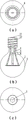
Accompanying drawing explanation
Fig. 1 (a), (b), (c) are rectangle crystalline ceramics COB substrate LED globular bulb structural representations of the present invention.
Fig. 2 (a), (b) are rectangle crystalline ceramics COB substrate structure schematic diagrames of the present invention
Fig. 3 (a), (b) are circular crystalline ceramics COB substrate structure schematic diagrames of the present invention
Fig. 4 (a), (b) are heating column schematic diagrames of the present invention
The specific embodiment
Technological means and effect of taking for reaching predetermined goal of the invention for further setting forth the present invention, below in conjunction with accompanying drawing and preferred embodiment, the crystalline ceramics COB substrate that utilizes proposing according to the present invention is realized to the encapsulating structure of comprehensive LED illumination, its specific embodiment, structure, feature and effect thereof, be described in detail as follows.
Refer to shown in Fig. 1 (a), (b), (c), the present invention adopts the structural design of crystalline ceramics as COB base plate for packaging, and it comprises: bulb 1, cathode contact 11, screw socket 12(cathode contact), heating column 2, positive wire 3, cathode wire 4, crystalline ceramics COB substrate 5.The upper end of bulb 1 is provided with screw socket 12, cathode contact 11 is arranged on screw socket 12(cathode contact 12) top, wire is leant on 2 central authorities that are located in bulb 1, positive wire 3, cathode wire 4 are separately positioned on the both sides of heating column 2, and positive wire 3 is connected with 11 of cathode contacts, cathode wire 4 is connected with 12 of screw sockets, and crystalline ceramics COB substrate 5 is connected with heating column 2, positive wire 3, cathode wire 4 respectively.
Refer to shown in Fig. 2 (a), (b) and Fig. 3 (a), (b), this crystalline ceramics COB substrate 5 adopts rectangle or circular configuration.It is layer structure, and the bottom is crystalline ceramics substrate 54, is silver slurry line layer 55 or copper base line layer on the upper strata of this crystalline ceramics substrate 54, and the upper strata of silver slurry line layer 55 or copper base line layer is LED chip 56.On crystalline ceramics COB substrate 5, be provided with three holes, its mesopore 51 is that anodal wiring hole, hole 52 are that galactic pole wiring hole, hole 53 are heating column installing hole.Aperture is designed according to wire thickness in its mesopore 51, hole 52, and starches line layer or copper base line layer circuit UNICOM with silver, and hole 53 is the heating column installing hole that high thermal conductivity alloy coordinates, and the dimensional tolerance in hole needs determine according to the thermal coefficient of expansion of ceramic and alloy.
Described crystalline ceramics substrate 54, is suitable for multiple system transparent ceramic material: as transparent alumina ceramics, transparent yttria ceramics, transparent YAG pottery, transparent AlON pottery etc.The COB ceramic substrate THICKNESS CONTROL of design is in 1mm left and right, and it is shaped as rectangle and circle shape.Can guarantee the light transmission that substrate is good, can make again substrate that heat is conducted and is delivered to fast high thermal conductivity alloy thermal column by heat, realize the perfect adaptation of printing opacity and heat radiation.
The material of described crystalline ceramics substrate 54, light transmittance: 30%--85%; Flatness (angularity) requires: the wide X of long X thick=the surface smoothness requirement of the transparent ceramic material of 120X120X1mm surface is less than 120um, to guarantee the adhesive force between money base circuit and substrate.On crystalline ceramics substrate, need process two fairleads according to wire thickness, with money base circuit UNICOM, centre processes the hole coordinating with high thermal conductivity alloy, and the dimensional tolerance in hole needs to determine according to the thermal coefficient of expansion of pottery and alloy.
The silver thickness of described silver slurry line layer 55 should be controlled at 0.1~0.3mm.
Refer to shown in Fig. 4 (a), (b), the material of described heating column 2 is elected aluminium or copper as.
The present embodiment adopts globular bulb profile, utilize crystalline ceramics substrate 54 as package cooling substrate, there is good light transmission, the light that LED sends not only can be sent before COB, and can send from its back side, thereby make the light angle of LED increase to 270 ° of left and right from 120 °~165 ° traditional left and right; The light efficiency of LED is brought up to 130 lumens from 100 lumens, energy-conservation 30% left and right of more traditional LED simultaneously.People's vision is more comfortable, is specially adapted to the intraoral illumination occasions such as the chamber such as family and office.
Following table has provided the strengths and weaknesses comparison of several base plate for packaging materials:
The above, it is only preferred embodiment of the present invention, not the present invention is done to any pro forma restriction, although the present invention discloses as above with preferred embodiment, but not in order to limit the present invention, any those skilled in the art, do not departing within the scope of technical solution of the present invention, when can utilizing the technology contents of above-mentioned announcement to make a little change or being modified to the equivalent embodiment of equivalent variations, in every case be the content that does not depart from technical solution of the present invention, any simple modification of above embodiment being done according to technical spirit of the present invention, equivalent variations and modification, all still belong in the scope of technical solution of the present invention.
Claims (6)
1. an encapsulating structure that utilizes crystalline ceramics COB substrate to realize comprehensive LED illumination, it comprises: bulb (1), cathode contact (11), screw socket (12), heating column (2), positive wire (3), cathode wire (4) characterized by further comprising crystalline ceramics COB substrate (5), and this crystalline ceramics COB substrate (5) is connected with heating column (2), positive wire (3), cathode wire (4) respectively.
2. the encapsulating structure that utilizes crystalline ceramics COB substrate to realize comprehensive LED illumination according to claim 1, it is characterized in that wherein said crystalline ceramics COB substrate (5) is for layer structure, the bottom is crystalline ceramics substrate (54), be silver slurry line layer or copper base line layer (55) on the upper strata of this crystalline ceramics substrate (54), the upper strata of silver slurry line layer (55) or copper base line layer is LED chip (56).
3. the encapsulating structure that utilizes crystalline ceramics COB substrate to realize comprehensive LED illumination according to claim 2, it is characterized in that being provided with three holes on crystalline ceramics COB substrate (5), its mesopore (51) is that anodal wiring hole, hole (52) are that galactic pole wiring hole, hole (53) are heating column installing hole, its mesopore (51), hole (52) are according to wire thickness design aperture, and starch line layer or copper base line layer circuit UNICOM with silver, hole (53) are the heating column installing hole that high thermal conductivity alloy coordinates.
4. realize the encapsulating structure of comprehensive LED illumination according to the crystalline ceramics COB substrate that utilizes described in arbitrary claim in claims 1 to 3, it is characterized in that described crystalline ceramics COB substrate (5) adopts rectangle or circular configuration.
5. the encapsulating structure that utilizes crystalline ceramics COB substrate to realize comprehensive LED illumination according to claim 1, the upper end that it is characterized in that described bulb (1) is provided with screw socket (12), cathode contact (11) is arranged on the top of screw socket (12), the central authorities of bulb 1 leant on (2) and are located in by wire, positive wire (3), cathode wire (4) are separately positioned on the both sides of heating column (2), and positive wire (3) is connected with cathode contact (11), cathode wire (4) is connected with screw socket (12).
6. the encapsulating structure that utilizes crystalline ceramics COB substrate to realize comprehensive LED illumination according to claim 1, the material that it is characterized in that heating column (2) is aluminium or copper.
Priority Applications (1)
| Application Number | Priority Date | Filing Date | Title |
|---|---|---|---|
| CN201210464576.4A CN103822104A (en) | 2012-11-16 | 2012-11-16 | All-dimensional LED illumination package structure implemented by aid of transparent ceramic COB (chip on board) substrate |
Applications Claiming Priority (1)
| Application Number | Priority Date | Filing Date | Title |
|---|---|---|---|
| CN201210464576.4A CN103822104A (en) | 2012-11-16 | 2012-11-16 | All-dimensional LED illumination package structure implemented by aid of transparent ceramic COB (chip on board) substrate |
Publications (1)
| Publication Number | Publication Date |
|---|---|
| CN103822104A true CN103822104A (en) | 2014-05-28 |
Family
ID=50757305
Family Applications (1)
| Application Number | Title | Priority Date | Filing Date |
|---|---|---|---|
| CN201210464576.4A Pending CN103822104A (en) | 2012-11-16 | 2012-11-16 | All-dimensional LED illumination package structure implemented by aid of transparent ceramic COB (chip on board) substrate |
Country Status (1)
| Country | Link |
|---|---|
| CN (1) | CN103822104A (en) |
Cited By (1)
| Publication number | Priority date | Publication date | Assignee | Title |
|---|---|---|---|---|
| CN105588024A (en) * | 2014-10-20 | 2016-05-18 | 深圳市晶联科技发展有限公司 | Efficient LED glass bulb lamp |
Citations (4)
| Publication number | Priority date | Publication date | Assignee | Title |
|---|---|---|---|---|
| US20070139949A1 (en) * | 2005-12-16 | 2007-06-21 | Nichia Corporation | Light emitting device |
| CN202048551U (en) * | 2011-05-16 | 2011-11-23 | 孙秀琴 | LED cooling module and lamps with the LED cooling module |
| CN202484663U (en) * | 2012-01-13 | 2012-10-10 | 长兴泛亚照明电器有限公司 | Large-angle LED (light-emitting diode) bulb lamp |
| CN202972633U (en) * | 2012-11-16 | 2013-06-05 | 洛阳欣珑陶瓷有限公司 | Packaging structure capable of realizing omni-directional LED (Light Emitting Diode) lighting by utilizing transparent ceramic COB (Chip on Board) substrate |
-
2012
- 2012-11-16 CN CN201210464576.4A patent/CN103822104A/en active Pending
Patent Citations (4)
| Publication number | Priority date | Publication date | Assignee | Title |
|---|---|---|---|---|
| US20070139949A1 (en) * | 2005-12-16 | 2007-06-21 | Nichia Corporation | Light emitting device |
| CN202048551U (en) * | 2011-05-16 | 2011-11-23 | 孙秀琴 | LED cooling module and lamps with the LED cooling module |
| CN202484663U (en) * | 2012-01-13 | 2012-10-10 | 长兴泛亚照明电器有限公司 | Large-angle LED (light-emitting diode) bulb lamp |
| CN202972633U (en) * | 2012-11-16 | 2013-06-05 | 洛阳欣珑陶瓷有限公司 | Packaging structure capable of realizing omni-directional LED (Light Emitting Diode) lighting by utilizing transparent ceramic COB (Chip on Board) substrate |
Cited By (1)
| Publication number | Priority date | Publication date | Assignee | Title |
|---|---|---|---|---|
| CN105588024A (en) * | 2014-10-20 | 2016-05-18 | 深圳市晶联科技发展有限公司 | Efficient LED glass bulb lamp |
Similar Documents
| Publication | Publication Date | Title |
|---|---|---|
| CN102291927B (en) | Ceramic substrate of LED (light-emitting diode) lamp and LED lamp | |
| CN202972633U (en) | Packaging structure capable of realizing omni-directional LED (Light Emitting Diode) lighting by utilizing transparent ceramic COB (Chip on Board) substrate | |
| CN101539250A (en) | LED lamp with high power | |
| CN203517379U (en) | Lamp bulb based on inversely-installed LED chips and transparent ceramic substrates | |
| CN102157507A (en) | White LED integration module with adjustable color temperature and color rendering indexes | |
| CN203260639U (en) | COB light source with high light efficiency and good heat dissipation | |
| CN103822104A (en) | All-dimensional LED illumination package structure implemented by aid of transparent ceramic COB (chip on board) substrate | |
| CN201103857Y (en) | An integrated LED light source assembly | |
| CN205956787U (en) | Thermoelectric separation type LED dot matrix light source | |
| CN203812909U (en) | LED filament transparent ceramic substrate | |
| CN203812908U (en) | LED lamp filament transparent glass substrate | |
| CN208111476U (en) | A thermoelectric separation type LED bracket | |
| CN206505946U (en) | A kind of LED/light source of specular removal | |
| CN205645861U (en) | Energy -conserving LED filament | |
| CN206364010U (en) | A kind of tunable optical COB light source encapsulated based on flip-over type | |
| CN203927821U (en) | A kind of high-efficiency heat radiating LED aluminium base | |
| CN204534218U (en) | The height heat radiation four sides light emitting LED lamp of a kind of light source and power supply one | |
| CN207741038U (en) | A kind of LED backlight of integration packaging | |
| CN205244870U (en) | LED ball bubble lamp of pottery module integration encapsulation | |
| CN222106707U (en) | A 7000W ultra-high power high-density color mixing light source | |
| CN203398113U (en) | Radiating ceramic packaged LED light source | |
| CN203631595U (en) | Insulating and radiating type light emitting diode | |
| CN204577460U (en) | Adopt the LED encapsulation structure of nitride multilayer aluminium base | |
| WO2012097653A1 (en) | 360 degree glowing led light | |
| CN202259291U (en) | An in-line multi-chip LED lamp bead |
Legal Events
| Date | Code | Title | Description |
|---|---|---|---|
| C06 | Publication | ||
| PB01 | Publication | ||
| C10 | Entry into substantive examination | ||
| SE01 | Entry into force of request for substantive examination | ||
| C02 | Deemed withdrawal of patent application after publication (patent law 2001) | ||
| WD01 | Invention patent application deemed withdrawn after publication |
Application publication date: 20140528 |