CN103762197A - Method for manufacturing novel Damascus copper and copper bonding structure - Google Patents
Method for manufacturing novel Damascus copper and copper bonding structure Download PDFInfo
- Publication number
- CN103762197A CN103762197A CN201310721130.XA CN201310721130A CN103762197A CN 103762197 A CN103762197 A CN 103762197A CN 201310721130 A CN201310721130 A CN 201310721130A CN 103762197 A CN103762197 A CN 103762197A
- Authority
- CN
- China
- Prior art keywords
- copper
- micro
- layer
- damascus
- novel
- Prior art date
- Legal status (The legal status is an assumption and is not a legal conclusion. Google has not performed a legal analysis and makes no representation as to the accuracy of the status listed.)
- Granted
Links
Images


Classifications
-
- H10W72/20—
-
- H10W72/012—
-
- H10W72/01251—
Landscapes
- Mechanical Treatment Of Semiconductor (AREA)
- Internal Circuitry In Semiconductor Integrated Circuit Devices (AREA)
Abstract
本发明提供了一种新型大马士革铜铜键合结构的制作方法,有效降低了铜柱表面粗糙度,提高了微凸点的表面平整度,保证了晶圆不同区域的微凸点高度的一致,满足铜铜键合工艺对表面平整度的要求,在后续的微组装工艺中不用做底填工艺,在降低工艺复杂度的同时,提高键合结构的可靠性,其特征在于:(1)在晶圆表面制作粘附层和种子层;(2)在晶圆表面淀积铜层;(3)对铜层进行图形化;(4)去除微凸点位置以外的铜形成微凸点结构;(5)去除微凸点区域以外的粘附层形成电隔离的微凸点结构;(6)去除光刻胶得到微凸点结构;(7)在微凸点结构间填充涂覆介质层;(8)对晶圆表面进行处理得到高度均匀,表面平坦光滑的介质层和外露的微凸点结构。
The invention provides a method for manufacturing a novel Damascus copper-copper bonding structure, which effectively reduces the surface roughness of copper pillars, improves the surface flatness of micro-bumps, and ensures the consistency of the heights of micro-bumps in different regions of the wafer. It meets the requirements of copper-copper bonding process for surface flatness, and does not need to do underfill process in the subsequent micro-assembly process. While reducing the complexity of the process, it improves the reliability of the bonding structure. It is characterized in that: (1) in Make an adhesion layer and a seed layer on the wafer surface; (2) Deposit a copper layer on the wafer surface; (3) Pattern the copper layer; (4) Remove copper other than the micro-bump position to form a micro-bump structure; (5) removing the adhesion layer outside the micro-bump area to form an electrically isolated micro-bump structure; (6) removing the photoresist to obtain the micro-bump structure; (7) filling the micro-bump structure with a coating medium layer; (8) Treat the surface of the wafer to obtain a highly uniform, flat and smooth dielectric layer and exposed micro-bump structure.
Description
技术领域 technical field
本发明涉及微电子封装技术领域,具体涉及一种新型大马士革铜铜键合结构的制作方法。 The invention relates to the technical field of microelectronic packaging, in particular to a method for manufacturing a novel damascene copper-copper bonding structure.
背景技术 Background technique
目前微凸点制作工艺在种子层制作后,利用光刻胶定义电镀区域。受微凸点高度限制,光刻胶厚度较大,从而导致传统的微凸点制作工艺在小尺寸微凸点制作上能力不足。此外,铜铜键合工艺对键合界面的平整度要求近乎苛刻,电镀工艺无法满足其要求。首先,电镀工艺生产的铜柱表面粗糙度较大,无法满足铜铜键合对表面平整度的要求;其次,电镀工艺制作的微凸点平整度较差,尤其是在下层有台阶的情况下,很难保证微凸点表面平整度;第三,采用传统工艺的微凸点技术,晶圆不同区域的微凸点高度会有较大差异,影响键合质量;第四,传统工艺的底填技术已经很难满足细节距、大面积的芯片微组装工艺,现有的细节距、大面积的芯片微组装工艺复杂,其工艺可靠性低。 The current micro-bump manufacturing process uses photoresist to define the electroplating area after the seed layer is manufactured. Limited by the height of the micro-bumps, the thickness of the photoresist is relatively large, which leads to the insufficient capability of the traditional micro-bump manufacturing process in the production of small-sized micro-bumps. In addition, the copper-copper bonding process has strict requirements on the flatness of the bonding interface, and the electroplating process cannot meet its requirements. First of all, the surface roughness of the copper pillars produced by the electroplating process is relatively large, which cannot meet the requirements of copper-copper bonding for surface flatness; secondly, the flatness of the micro-bumps produced by the electroplating process is poor, especially when there are steps in the lower layer , it is difficult to ensure the flatness of the micro-bump surface; third, the height of the micro-bumps in different regions of the wafer will have a large difference with the micro-bump technology of the traditional process, which will affect the bonding quality; fourth, the bottom of the traditional process Filling technology has been difficult to meet the fine-pitch, large-area chip micro-assembly process, the existing fine-pitch, large-area chip micro-assembly process is complicated, and its process reliability is low.
发明内容 Contents of the invention
针对上述问题,本发明提供了一种新型大马士革铜铜键合结构的制作方法,有效降低了铜柱表面粗糙度,提高了微凸点的表面平整度,同时保证了晶圆不同区域的微凸点高度的一致,而且在后续的微组装工艺中不用做底填工艺,可以在降低工艺难度的同时,提高键合结构的可靠性。 In view of the above problems, the present invention provides a novel method for fabricating a Damascus copper-copper bonding structure, which effectively reduces the surface roughness of copper pillars, improves the surface flatness of micro-bumps, and at the same time ensures the micro-bumps in different regions of the wafer. The point height is consistent, and no underfill process is required in the subsequent micro-assembly process, which can improve the reliability of the bonding structure while reducing the difficulty of the process.
其技术方案如下: Its technical scheme is as follows:
一种新型大马士革铜铜键合结构的制作方法,其包括以下步骤: A kind of manufacture method of novel Damascus copper-copper bonding structure, it comprises the following steps:
(1)、在晶圆表面制作粘附层和种子层; (1) Fabricate an adhesion layer and a seed layer on the wafer surface;
(2)、在晶圆表面淀积铜层; (2) Deposit a copper layer on the wafer surface;
(3)、利用光刻工艺对铜层进行图形化; (3) Patterning the copper layer by photolithography;
(4)、去除微凸点位置以外的铜,在晶圆上形成微凸点结构; (4) Remove the copper outside the micro-bump position and form a micro-bump structure on the wafer;
(5)、去除晶圆表面微凸点区域以外的粘附层材料,形成电隔离的微凸点结构; (5) Remove the adhesion layer material outside the micro-bump area on the wafer surface to form an electrically isolated micro-bump structure;
(6)、去除晶圆表面的光刻胶,得到去胶后的微凸点结构; (6) Remove the photoresist on the surface of the wafer to obtain the micro-bump structure after removing the glue;
(7)、在晶圆表面微凸点结构之间填充、涂覆介质层; (7) Fill and coat the dielectric layer between the micro-bump structures on the wafer surface;
(8)、对晶圆表面进行处理,去除多余的介质层材料,对晶圆表面的介质层和铜柱进行抛光加工,得到高度均匀,表面平坦光滑的介质层和外露的微凸点结构; (8) Treat the surface of the wafer, remove excess dielectric layer material, and polish the dielectric layer and copper pillars on the wafer surface to obtain a highly uniform, flat and smooth dielectric layer and exposed micro-bump structure;
其更进一步地还包括以下步骤: It further includes the following steps:
(9)、利用铜铜键合工艺将两个芯片键合在一起,利用铜柱间已经填充介质形成支撑; (9) Use copper-copper bonding technology to bond the two chips together, and use the medium filled between the copper pillars to form a support;
其更进一步在于:步骤(2)中,利用电镀工艺在晶圆表面淀积铜层; It further lies in that: in step (2), a copper layer is deposited on the surface of the wafer by electroplating;
步骤(4)中,利用电解工艺去除微凸点位置以外的铜,在晶圆上形成微凸点结构; In step (4), the electrolytic process is used to remove the copper other than the position of the micro-bump, and a micro-bump structure is formed on the wafer;
步骤(5)中,利用湿法刻蚀工艺去除晶圆表面微凸点区域以外的粘附层材料,形成电隔离的微凸点结构; In step (5), a wet etching process is used to remove the adhesion layer material outside the micro-bump area on the wafer surface to form an electrically isolated micro-bump structure;
步骤(8)中,利用化学机械抛光工艺对晶圆表面进行处理,去除多余的介质层材料,并对晶圆表面进行平坦化处理,露出微凸点。 In step (8), the surface of the wafer is treated by a chemical mechanical polishing process to remove excess dielectric material, and the surface of the wafer is planarized to expose the micro-bumps.
采用本发明的上述方法中,先淀积铜层,然后利用光刻和电化学抛光工艺去除多余部分的铜金属层,成型微凸点,并借助于化学机械抛光工艺,有效降低了铜柱表面粗糙度,提高了微凸点的表面平整度,保证了晶圆不同区域的微凸点高度一致并且表面光滑。 In the above-mentioned method of the present invention, the copper layer is first deposited, and then the redundant part of the copper metal layer is removed by photolithography and electrochemical polishing processes, and the micro-bumps are formed, and the surface of the copper pillars is effectively reduced by means of the chemical mechanical polishing process. The roughness improves the surface flatness of the micro-bumps, and ensures that the height of the micro-bumps in different regions of the wafer is consistent and the surface is smooth.
随着微组装结构尺寸的不断减小,芯片尺寸的进一步增大,底填工艺的难度越来越大,本专利提出的工艺方案在后续的微组装工艺中不用做底填工艺,可以在降低工艺复杂度的同时,提高键合结构的可靠性。 With the continuous reduction of the size of the micro-assembly structure and the further increase of the chip size, the difficulty of the underfill process is becoming more and more difficult. The process scheme proposed in this patent does not require the underfill process in the subsequent micro-assembly process, which can reduce the While reducing the complexity of the process, the reliability of the bonding structure is improved.
附图说明 Description of drawings
图1为晶圆表面制作粘附层和种子层示意图; Figure 1 is a schematic diagram of making an adhesion layer and a seed layer on the wafer surface;
图2为晶圆表面淀积铜层示意图; Fig. 2 is a schematic diagram of depositing a copper layer on a wafer surface;
图3为对微凸点进行定义示意图; Fig. 3 is a schematic diagram of defining micro-bumps;
图4为晶圆上形成微凸点示意图; 4 is a schematic diagram of forming micro-bumps on a wafer;
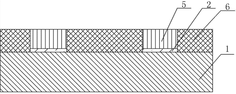
图5为去除晶圆表面微凸点区域以外的粘附层材料示意图; Fig. 5 is the schematic diagram of removing the adhesive layer material outside the micro-bump area on the wafer surface;
图6为去除晶圆表面的光刻胶成型光滑的微凸点示意图; Figure 6 is a schematic diagram of removing the photoresist on the surface of the wafer to form a smooth micro-bump;
图7为晶圆表面涂覆介质层示意图; 7 is a schematic diagram of a dielectric layer coated on the surface of a wafer;
图8为去除介质层露出微凸点示意图; Figure 8 is a schematic diagram of removing the dielectric layer to expose the micro-bumps;
图9 铜铜键合后效果图。 Figure 9 Effect diagram of copper-copper bonding.
具体实施方式 Detailed ways
一种新型大马士革铜铜键合结构的制作方法,其特征在于:其包括以下步骤: A method for making a novel Damascus copper-copper bonding structure, characterized in that it comprises the following steps:
见图1,(1)在晶圆1表面制作粘附层2和种子层3-1,粘附层材料可以是钛、氮化钛、钽、氮化钽等材料的一种或多种材料,种子层材料为铜。(晶圆上已经制作完成器件和互联结构制作);
See Figure 1, (1) Fabricate an
见图2,(2)利用电镀工艺在晶圆表面淀积铜层3-2,铜层厚度为1-15μm; See Figure 2, (2) Deposit a copper layer 3-2 on the surface of the wafer by electroplating process, the thickness of the copper layer is 1-15μm;
见图3,(3)利用光刻工艺对铜层表面进行图形化; See Figure 3, (3) pattern the surface of the copper layer by photolithography;
见图4,(4)利用电解工艺去除微凸点位置以外的铜,在晶圆上形成微凸点结构5,该工艺将晶圆上的铜与电源的阳极相连,一般采用酸性电解液,并在电解液中通电,使晶圆表面裸露的铜电解;
See Figure 4, (4) Use electrolytic process to remove copper outside the position of the micro-bump, and form a
见图5,(5)利用湿法刻蚀工艺去除晶圆表面微凸点区域以外的粘附层2,形成电隔离的微凸点结构5;
As shown in Fig. 5, (5) using a wet etching process to remove the
见图6,(6)去除晶圆表面的光刻胶4,得到微凸点结构5;
See Fig. 6, (6) remove the photoresist 4 on the surface of the wafer to obtain the
见图7,(7)晶圆表面微凸点结构之间填充、涂覆介质层6;介质层的材料可以是二氧化硅、氮化硅、聚酰亚胺、聚对苯撑苯并双口恶唑纤维材料等材料;
See Figure 7, (7)
见图8,(8)利用化学机械抛光工艺对晶圆表面进行处理,去除多余的介质层6,对晶圆表面的介质层和铜柱进行抛光加工,得到高度均匀,表面平坦光滑的介质层和外露的微凸点结构5;
See Figure 8, (8) Treat the wafer surface by chemical mechanical polishing process, remove the excess
见图9,(9)借助于步骤(8)形成的平坦均匀的铜柱结构,第一晶圆7-1和第二晶圆7-2片完成铜铜键合,所以无需底填工艺,工艺难度低,可靠性好。 See Figure 9, (9) With the help of the flat and uniform copper pillar structure formed in step (8), the copper-copper bonding of the first wafer 7-1 and the second wafer 7-2 is completed, so no underfill process is required, The process difficulty is low and the reliability is good.
本专利的上述方法中,采用单次CMP工艺完成大马士革工艺,工艺成难度低,处理后的大马士革结构表面平整光滑,可满足铜铜键合工艺要求。 In the above-mentioned method of this patent, a single CMP process is used to complete the damascene process, and the difficulty of the process is low. The surface of the treated damascene structure is smooth and smooth, which can meet the requirements of the copper-copper bonding process.
随着微组装结构尺寸的不断减小,芯片尺寸的进一步增大,底填工艺的难度越来越大,步骤(7)、步骤(8)和步骤(9)中,成型微凸点结构5外侧的介质绝缘材料,露出微凸点的待连接部位,借助于步骤(8)形成的平坦均匀的铜柱结构,步骤(9)中第一晶圆7-1和第二晶圆7-2完成铜铜键合,由于铜柱间已经填充介质,使其可以实现超细节距的铜铜键合,使得微凸点可以直接进行连接,所提出的工艺方案在后续的微组装工艺中不用做底填工艺,可以在降低工艺难度的同时,提高键合结构的可靠性。
With the continuous reduction of the size of the micro-assembly structure and the further increase of the chip size, the underfill process becomes more and more difficult. In step (7), step (8) and step (9), the
Claims (9)
Priority Applications (1)
| Application Number | Priority Date | Filing Date | Title |
|---|---|---|---|
| CN201310721130.XA CN103762197B (en) | 2013-12-24 | 2013-12-24 | The manufacture method of a kind of novel Damascus copper copper bonding structure |
Applications Claiming Priority (1)
| Application Number | Priority Date | Filing Date | Title |
|---|---|---|---|
| CN201310721130.XA CN103762197B (en) | 2013-12-24 | 2013-12-24 | The manufacture method of a kind of novel Damascus copper copper bonding structure |
Publications (2)
| Publication Number | Publication Date |
|---|---|
| CN103762197A true CN103762197A (en) | 2014-04-30 |
| CN103762197B CN103762197B (en) | 2016-03-16 |
Family
ID=50529410
Family Applications (1)
| Application Number | Title | Priority Date | Filing Date |
|---|---|---|---|
| CN201310721130.XA Active CN103762197B (en) | 2013-12-24 | 2013-12-24 | The manufacture method of a kind of novel Damascus copper copper bonding structure |
Country Status (1)
| Country | Link |
|---|---|
| CN (1) | CN103762197B (en) |
Cited By (6)
| Publication number | Priority date | Publication date | Assignee | Title |
|---|---|---|---|---|
| CN104637831A (en) * | 2015-02-12 | 2015-05-20 | 华中科技大学 | Copper nanometer wire-based copper-copper bonding process |
| CN105006440A (en) * | 2015-06-24 | 2015-10-28 | 武汉新芯集成电路制造有限公司 | Vacuum-bonding atmospheric-pressurization hybrid bonding method |
| CN106521573A (en) * | 2016-11-23 | 2017-03-22 | 苏州昕皓新材料科技有限公司 | Method for producing electroplated copper layer with preferential orientation growth structure, and application thereof |
| CN110504174A (en) * | 2019-07-25 | 2019-11-26 | 南通通富微电子有限公司 | The forming method of encapsulating structure |
| CN111599704A (en) * | 2020-06-01 | 2020-08-28 | 深圳市美科泰科技有限公司 | Method for constructing salient points of integrated circuit |
| CN119626914A (en) * | 2025-02-13 | 2025-03-14 | 江苏中科智芯集成科技有限公司 | Low temperature bonding method for chips |
Citations (6)
| Publication number | Priority date | Publication date | Assignee | Title |
|---|---|---|---|---|
| CN102543898A (en) * | 2012-01-17 | 2012-07-04 | 南通富士通微电子股份有限公司 | Cylindrical bump packaging structure |
| CN102543766A (en) * | 2012-01-17 | 2012-07-04 | 南通富士通微电子股份有限公司 | Columnar bump packaging process |
| CN102593087A (en) * | 2012-03-01 | 2012-07-18 | 江苏物联网研究发展中心 | Mixed bonding structure for three-dimension integration and bonding method for mixed bonding structure |
| CN103165524A (en) * | 2013-04-03 | 2013-06-19 | 株洲南车时代电气股份有限公司 | Insulated gate bipolar translator (IGBT) chip and manufacturing method of copper metallization structure on right side of IGBT chip |
| CN103311131A (en) * | 2013-05-15 | 2013-09-18 | 华进半导体封装先导技术研发中心有限公司 | Method for preventing lateral undercutting of micro-convex points in manufacturing process of micro-convex points |
| CN103456652A (en) * | 2013-09-13 | 2013-12-18 | 华进半导体封装先导技术研发中心有限公司 | Mixed bonding implementation method |
-
2013
- 2013-12-24 CN CN201310721130.XA patent/CN103762197B/en active Active
Patent Citations (6)
| Publication number | Priority date | Publication date | Assignee | Title |
|---|---|---|---|---|
| CN102543898A (en) * | 2012-01-17 | 2012-07-04 | 南通富士通微电子股份有限公司 | Cylindrical bump packaging structure |
| CN102543766A (en) * | 2012-01-17 | 2012-07-04 | 南通富士通微电子股份有限公司 | Columnar bump packaging process |
| CN102593087A (en) * | 2012-03-01 | 2012-07-18 | 江苏物联网研究发展中心 | Mixed bonding structure for three-dimension integration and bonding method for mixed bonding structure |
| CN103165524A (en) * | 2013-04-03 | 2013-06-19 | 株洲南车时代电气股份有限公司 | Insulated gate bipolar translator (IGBT) chip and manufacturing method of copper metallization structure on right side of IGBT chip |
| CN103311131A (en) * | 2013-05-15 | 2013-09-18 | 华进半导体封装先导技术研发中心有限公司 | Method for preventing lateral undercutting of micro-convex points in manufacturing process of micro-convex points |
| CN103456652A (en) * | 2013-09-13 | 2013-12-18 | 华进半导体封装先导技术研发中心有限公司 | Mixed bonding implementation method |
Cited By (11)
| Publication number | Priority date | Publication date | Assignee | Title |
|---|---|---|---|---|
| CN104637831A (en) * | 2015-02-12 | 2015-05-20 | 华中科技大学 | Copper nanometer wire-based copper-copper bonding process |
| CN104637831B (en) * | 2015-02-12 | 2017-06-27 | 华中科技大学 | A kind of copper copper bonding technology based on copper nano-wire |
| CN105006440A (en) * | 2015-06-24 | 2015-10-28 | 武汉新芯集成电路制造有限公司 | Vacuum-bonding atmospheric-pressurization hybrid bonding method |
| CN105006440B (en) * | 2015-06-24 | 2018-01-09 | 武汉新芯集成电路制造有限公司 | A kind of hybrid bonded method of vacuum bonding air pressurization |
| CN106521573A (en) * | 2016-11-23 | 2017-03-22 | 苏州昕皓新材料科技有限公司 | Method for producing electroplated copper layer with preferential orientation growth structure, and application thereof |
| CN106521573B (en) * | 2016-11-23 | 2019-10-01 | 苏州昕皓新材料科技有限公司 | Prepare the method and its application with the copper electroplating layer of preferred orientation growth structure |
| CN110504174A (en) * | 2019-07-25 | 2019-11-26 | 南通通富微电子有限公司 | The forming method of encapsulating structure |
| CN111599704A (en) * | 2020-06-01 | 2020-08-28 | 深圳市美科泰科技有限公司 | Method for constructing salient points of integrated circuit |
| CN111599704B (en) * | 2020-06-01 | 2022-06-28 | 深圳市美科泰科技有限公司 | A method of constructing an integrated circuit bump |
| CN119626914A (en) * | 2025-02-13 | 2025-03-14 | 江苏中科智芯集成科技有限公司 | Low temperature bonding method for chips |
| CN119626914B (en) * | 2025-02-13 | 2025-06-17 | 江苏中科智芯集成科技有限公司 | Low temperature bonding method for chips |
Also Published As
| Publication number | Publication date |
|---|---|
| CN103762197B (en) | 2016-03-16 |
Similar Documents
| Publication | Publication Date | Title |
|---|---|---|
| US8697493B2 (en) | Bonding surfaces for direct bonding of semiconductor structures | |
| CN102820257B (en) | Through silicon via structure and method | |
| CN103762197B (en) | The manufacture method of a kind of novel Damascus copper copper bonding structure | |
| TW202518682A (en) | Methods and structures for low temperature hybrid bonding | |
| US10804151B2 (en) | Systems and methods for producing flat surfaces in interconnect structures | |
| TW201110306A (en) | 3D multi-wafer stacked semiconductor structure and method for manufacturing the same | |
| TW201145493A (en) | Silicon wafer structure and multi-chip stack structure | |
| CN103730382B (en) | A kind of manufacture method of copper-copper bonding salient points | |
| CN103280427B (en) | A kind of TSV front side end interconnection process | |
| CN103258791B (en) | Method and the corresponding device of metal interconnection is realized by preparing ultra fine-pitch micro convex point | |
| CN103456685A (en) | Manufacturing method for TSV and first layer re-wiring layer needless of using CMP | |
| CN108063097A (en) | A kind of three layers of integrated chip method | |
| CN104347481A (en) | Metal coating processing method | |
| CN103441111A (en) | Three-dimensional packaging interconnection structure and manufacturing method thereof | |
| TW201308576A (en) | Improved bond surface for direct bonding of semiconductor structures | |
| CN105140143A (en) | Wafer bonding process | |
| CN103474393B (en) | Electroplating process capable of removing copper layer and reusing barrier layer without CMP | |
| CN104900543B (en) | A kind of semiconductor devices and preparation method thereof | |
| CN104637862B (en) | Semiconductor Structure Formation Method | |
| CN108054137B (en) | Metal interconnection structure and manufacturing method thereof | |
| US20140238725A1 (en) | Method of flattening surface of conductive structure and conductive structure with flattened surface | |
| CN104143525A (en) | Method for flattening through-silicon-via back-surface metal | |
| CN101894766B (en) | Method for manufacturing solder lug | |
| CN109346419B (en) | Semiconductor device and method of manufacturing the same | |
| CN103295915B (en) | The manufacture method of TSV keyset and TSV keyset |
Legal Events
| Date | Code | Title | Description |
|---|---|---|---|
| C06 | Publication | ||
| PB01 | Publication | ||
| C10 | Entry into substantive examination | ||
| SE01 | Entry into force of request for substantive examination | ||
| C14 | Grant of patent or utility model | ||
| GR01 | Patent grant | ||
| EE01 | Entry into force of recordation of patent licensing contract |
Application publication date: 20140430 Assignee: Jiangsu Xinde Semiconductor Technology Co.,Ltd. Assignor: National Center for Advanced Packaging Co.,Ltd. Contract record no.: X2022980027357 Denomination of invention: Fabrication of a new Damascus copper copper bonding structure Granted publication date: 20160316 License type: Common License Record date: 20221213 |
|
| EE01 | Entry into force of recordation of patent licensing contract |