CN103517625A - Memory apparatus and electronic apparatus - Google Patents
Memory apparatus and electronic apparatus Download PDFInfo
- Publication number
- CN103517625A CN103517625A CN201310238021.2A CN201310238021A CN103517625A CN 103517625 A CN103517625 A CN 103517625A CN 201310238021 A CN201310238021 A CN 201310238021A CN 103517625 A CN103517625 A CN 103517625A
- Authority
- CN
- China
- Prior art keywords
- memory
- circuit board
- electronic device
- terminals
- terminal
- Prior art date
- Legal status (The legal status is an assumption and is not a legal conclusion. Google has not performed a legal analysis and makes no representation as to the accuracy of the status listed.)
- Pending
Links
Images


Classifications
-
- H—ELECTRICITY
- H03—ELECTRONIC CIRCUITRY
- H03K—PULSE TECHNIQUE
- H03K3/00—Circuits for generating electric pulses; Monostable, bistable or multistable circuits
- H03K3/01—Details
- H03K3/013—Modifications of generator to prevent operation by noise or interference
-
- G—PHYSICS
- G06—COMPUTING OR CALCULATING; COUNTING
- G06F—ELECTRIC DIGITAL DATA PROCESSING
- G06F1/00—Details not covered by groups G06F3/00 - G06F13/00 and G06F21/00
- G06F1/16—Constructional details or arrangements
- G06F1/18—Packaging or power distribution
- G06F1/183—Internal mounting support structures, e.g. for printed circuit boards, internal connecting means
- G06F1/185—Mounting of expansion boards
-
- G—PHYSICS
- G06—COMPUTING OR CALCULATING; COUNTING
- G06F—ELECTRIC DIGITAL DATA PROCESSING
- G06F1/00—Details not covered by groups G06F3/00 - G06F13/00 and G06F21/00
- G06F1/16—Constructional details or arrangements
-
- G—PHYSICS
- G06—COMPUTING OR CALCULATING; COUNTING
- G06F—ELECTRIC DIGITAL DATA PROCESSING
- G06F13/00—Interconnection of, or transfer of information or other signals between, memories, input/output devices or central processing units
- G06F13/38—Information transfer, e.g. on bus
- G06F13/40—Bus structure
- G06F13/4063—Device-to-bus coupling
- G06F13/409—Mechanical coupling
-
- G—PHYSICS
- G11—INFORMATION STORAGE
- G11C—STATIC STORES
- G11C5/00—Details of stores covered by group G11C11/00
- G11C5/02—Disposition of storage elements, e.g. in the form of a matrix array
- G11C5/04—Supports for storage elements, e.g. memory modules; Mounting or fixing of storage elements on such supports
Landscapes
- Engineering & Computer Science (AREA)
- Theoretical Computer Science (AREA)
- General Engineering & Computer Science (AREA)
- Physics & Mathematics (AREA)
- General Physics & Mathematics (AREA)
- Computer Hardware Design (AREA)
- Human Computer Interaction (AREA)
- Power Engineering (AREA)
- Structures For Mounting Electric Components On Printed Circuit Boards (AREA)
- Coupling Device And Connection With Printed Circuit (AREA)
- Shielding Devices Or Components To Electric Or Magnetic Fields (AREA)
Abstract
一种存储器设备,包括电路板、具有布置在电路板上的多个存储器芯片的存储器部分、提供电子设备和布置在电路板第一侧的多个存储器芯片之间的接口的端子,以及连接部分,所述连接部分连接电子设备的固定单元以将存储器设备固定至电子设备,所述连接部分布置在电路板的第二侧以便面对端子。
A memory device comprising a circuit board, a memory section having a plurality of memory chips arranged on the circuit board, a terminal providing an interface between the electronic device and the plurality of memory chips arranged on a first side of the circuit board, and a connection section , the connection part connects the fixing unit of the electronic device to fix the memory device to the electronic device, the connection part is arranged on the second side of the circuit board so as to face the terminal.
Description
相关申请的交叉引用Cross References to Related Applications
本申请要求在2012年6月18日和2013年4月23日分别向韩国专利局递交的专利申请No.10-2012-0065117和No.10-2013-0044942的优先权,其全部内容通过参考合并于此。This application claims priority to Patent Applications No. 10-2012-0065117 and No. 10-2013-0044942 filed with the Korean Patent Office on Jun. 18, 2012 and Apr. 23, 2013, the entire contents of which are incorporated by reference merged here.
技术领域technical field
根据本公开的设备涉及存储器设备和电子设备,更具体地,涉及小尺寸的存储器设备和电子设备。Devices according to the present disclosure relate to memory devices and electronic devices, and more particularly, to small-sized memory devices and electronic devices.
背景技术Background technique
膝上型电脑通常称为笔记本电脑,其便于个人用户携带和使用。最近,膝上型PC或平板型产品的“轻薄”特征正不断地得以加强。Laptop computers, commonly referred to as notebook computers, are convenient for personal users to carry and use. Recently, "thin and light" features of laptop PCs or tablet-type products are being continuously enhanced.
随着“轻薄”倾向的增强和高速且高集成存储器技术的实现,已经提出需要改进到迄今已使用的PC的存储器模块,并且还提议进行技术和经济上的改进。With the enhancement of "thin and light" tendency and the realization of high-speed and highly integrated memory technology, improvement to the memory modules of PCs that have been used hitherto has been proposed, and technical and economical improvements have also been proposed.
此外,由于高速存储器模块的实现,随存储器的操作发生的射频干扰(RFI)噪声的问题与过去相比越来越成问题。因此,需要一种方法,其可以解决RFI噪声问题。Furthermore, due to the implementation of high-speed memory modules, the problem of radio frequency interference (RFI) noise occurring with the operation of the memory is more problematic than in the past. Therefore, there is a need for a method that can solve the RFI noise problem.
发明内容Contents of the invention
本发明总构思克服了上述缺点以及上面没有提到的其他缺点。此外,本发明总构思不必克服上述缺点,并且本发明总构思的示例实施例可以不克服上述任一个问题。The present general inventive concept overcomes the above disadvantages and other disadvantages not mentioned above. Also, the present general inventive concept is not required to overcome the disadvantages described above, and an exemplary embodiment of the present general inventive concept may not overcome any of the problems described above.
本发明总构思的技术目的在于提供一种具有小尺寸的存储器设备和电子设备。A technical purpose of the present general inventive concept is to provide a memory device and an electronic device having a small size.
本发明总构思的另一技术目的在于提供一种存储器设备和电子设备,其降低在存储器设备中可能发生的射频干扰(RFI)噪声。Another technical object of the present general inventive concept is to provide a memory device and an electronic device that reduce radio frequency interference (RFI) noise that may occur in the memory device.
本发明总构思的其他特征和用途将在下面的说明书中部分地给出,并从说明书中部分地变得清楚,或可以通过本发明总构思的实践而获知。Other features and uses of the general concept of the present invention will be partly given in the following description, and partly become clear from the description, or can be known through the practice of the general concept of the present invention.
通过提供一种安装在电子设备上的存储器设备实现本发明总构思的前述的和/或其他特征和用途,所述存储器设备包括电路板、包括布置在电路板上的多个存储器芯片的存储器部分、布置在电路板的第一侧以提供电子设备和多个存储器芯片之间的接口的端子、以及连接部分,布置在电路板的第二侧以面对所述端子,所述连接部分连接至电子设备的固定(fixing)单元以将存储器设备固定至电子设备,并且布置在电路板的另一侧以便面对所述端子。The foregoing and/or other features and uses of the present general inventive concept are achieved by providing a memory device mounted on an electronic device, the memory device comprising a circuit board, a memory portion comprising a plurality of memory chips arranged on the circuit board , a terminal arranged on a first side of the circuit board to provide an interface between the electronic device and a plurality of memory chips, and a connecting portion arranged on a second side of the circuit board to face the terminal, the connecting portion being connected to A fixing unit of the electronic device to fix the memory device to the electronic device, and is arranged on the other side of the circuit board so as to face the terminals.
电路板可以具有50mm至60mm的水平长度和15mm至25mm的垂直长度。The circuit board may have a horizontal length of 50mm to 60mm and a vertical length of 15mm to 25mm.
存储器部分和布置了存储器部分的电路板的厚度为3mm至4mm。。The memory portion and the circuit board on which the memory portion is arranged have a thickness of 3 mm to 4 mm. .
端子可以包括:第一端子,包括在电路板的上部以均匀间隔分隔开的多个端子;和第二端子,包括在电路板的上部以均匀间隔分隔开的多个端子。The terminals may include: first terminals including a plurality of terminals spaced at uniform intervals on the upper portion of the circuit board; and second terminals including a plurality of terminals spaced at even intervals on the upper portion of the circuit board.
第一端子的多个端子之间的间隔和第二端子的多个端子之间的间隔可以分别是0.5mm。The intervals between the plurality of terminals of the first terminal and the intervals between the plurality of terminals of the second terminal may be 0.5 mm, respectively.
第一端子和第二端子彼此分隔开。The first terminal and the second terminal are spaced apart from each other.
第一端子和第二端子之间插入在其间形成的槽。A groove formed therebetween is interposed between the first terminal and the second terminal.
第一端子的端子和第二端子的相邻端子之间的间隔是与第一端子的多个端子之间的间隔相同的间隔。An interval between a terminal of the first terminal and an adjacent terminal of the second terminal is the same interval as an interval between a plurality of terminals of the first terminal.
所述端子包括多个端子,并且所述多个端子是170至200个端子。The terminals include a plurality of terminals, and the plurality of terminals is 170 to 200 terminals.
所述连接部分被实现为在电路板的第二侧的具有预设尺寸的槽。The connecting portion is realized as a slot having a predetermined size on the second side of the circuit board.
连接部分的位置与可附着至电子设备的存储器模块的类型对应。The location of the connection portion corresponds to the type of memory module attachable to the electronic device.
多个存储器芯片布置在电路板的相同侧表面上。A plurality of memory chips are arranged on the same side surface of the circuit board.
多个存储器芯片可以布置在电路板的两个侧表面上。A plurality of memory chips may be arranged on both side surfaces of the circuit board.
存储器设备可以附加地包括屏蔽件,其密封电路板的上部。The memory device may additionally include a shield that seals the upper portion of the circuit board.
屏蔽件可以由金属形成。The shield may be formed of metal.
本发明总构思的前述和/或其他特征和用途还可以通过提供一种安装至电子设备的存储器设备实现,所述存储器设备包括电路板、包括布置在电路板上的多个存储器芯片的存储器部分、以及布置在电路板的第一侧以提供电子设备和多个存储器芯片之间的接口的端子。电路板可以具有50mm至60mm的水平长度和15mm至25mm的垂直长度。The foregoing and/or other features and uses of the present general inventive concept can also be achieved by providing a memory device mounted to an electronic device, the memory device comprising a circuit board, a memory portion comprising a plurality of memory chips arranged on the circuit board , and terminals disposed on the first side of the circuit board to provide an interface between the electronic device and the plurality of memory chips. The circuit board may have a horizontal length of 50mm to 60mm and a vertical length of 15mm to 25mm.
本发明总构思的前述和/或其他特征和用途还可以通过提供一种存储器模块可附着至或从其可拆卸的电子设备来实现,所述电子设备包括:插口,包括电连接至存储器模块的多个端子;固定单元,将存储器模块固定至电子设备。固定单元关于存储器模块与插口相对地布置。The foregoing and/or other features and uses of the present general inventive concept can also be achieved by providing an electronic device to which a memory module is attachable or detachable, the electronic device comprising: a socket including a socket electrically connected to the memory module A plurality of terminals; a fixing unit to fix the memory module to the electronic device. The fixing unit is arranged opposite to the socket with respect to the memory module.
多个端子可以包括第一端子和第二端子,第一端子包括在插口的第一侧以均匀间隔分隔开的多个端子,第二端子包括在插口的第二侧以均匀间隔分隔开的多个端子。The plurality of terminals may include a first terminal comprising a plurality of terminals spaced at even intervals on a first side of the receptacle and a second terminal comprising a plurality of terminals spaced at even intervals on a second side of the receptacle. multiple terminals.
第一端子的多个端子之间的间隔和第二端子的多个端子之间的间隔可以分别是0.5mm。The intervals between the plurality of terminals of the first terminal and the intervals between the plurality of terminals of the second terminal may be 0.5 mm, respectively.
第一端子和第二端子彼此分隔开。The first terminal and the second terminal are spaced apart from each other.
第一端子的端子和第二端子的相邻端子之间的间隔可以是与第一端子的多个端子之间的间隔相同的间隔。An interval between a terminal of the first terminal and an adjacent terminal of the second terminal may be the same interval as an interval between a plurality of terminals of the first terminal.
固定单元的位置可以与可附着至电子设备的存储器模块的类型对应。The location of the fixing unit may correspond to the type of memory module attachable to the electronic device.
电子设备可以附加地包括屏蔽件以防止存储器模块的噪声进入电子设备。The electronic device may additionally include a shield to prevent noise of the memory module from entering the electronic device.
屏蔽件可以由金属形成。The shield may be formed of metal.
屏蔽件可以与电子设备是可分离的并且通过固定单元固定。The shield may be detachable from the electronic device and fixed by the fixing unit.
电子设备可以附加地包括布置在插口和固定单元之间的多个存储器芯片。The electronic device may additionally include a plurality of memory chips arranged between the socket and the fixing unit.
本发明总构思的前述和/或其他特征和用途还可以通过提供一种存储器模块可附着至或从其可拆卸的电子设备来实现,所述电子设备包括:插口,包括电连接至存储器模块的多个端子;固定单元,将存储器模块固定至电子设备;以及屏蔽件,去除存储器模块的噪声。屏蔽件可以从电子设备分离并通过固定单元固定。The foregoing and/or other features and uses of the present general inventive concept can also be achieved by providing an electronic device to which a memory module is attachable or detachable, the electronic device comprising: a socket including a socket electrically connected to the memory module A plurality of terminals; a fixing unit to fix the memory module to the electronic device; and a shield to remove noise of the memory module. The shield may be separated from the electronic device and fixed by the fixing unit.
本发明总构思的前述和/或其他特征和用途还可以通过提供一种存储器模块可附着至或从其可拆卸的电子设备来实现,所述电子设备包括:插口,包括电连接至存储器模块的多个端子;固定单元,将存储器模块固定至电子设备;以及屏蔽件,去除存储器模块的噪声。此外,屏蔽件可以从电子设备分离并通过固定单元固定。The foregoing and/or other features and uses of the present general inventive concept can also be achieved by providing an electronic device to which a memory module is attachable or detachable, the electronic device comprising: a socket including a socket electrically connected to the memory module A plurality of terminals; a fixing unit to fix the memory module to the electronic device; and a shield to remove noise of the memory module. Also, the shield may be separated from the electronic device and fixed by the fixing unit.
本发明总构思的前述的和/或其他特征和应用还可以通过提供一种存储器设备来实现,所述存储器设备包括电路板、安装在电路板上的多个存储器芯片、设置在电路板的第一侧并且包括用以在存储器设备和电子设备之间提供接口的多个端子的端子部分、以及设置在电路板的第二侧的连接部分,连接部分布置成可移除地连接电子设备的固定单元以将存储器设备固定至电子设备或从电子设备移除存储器设备。The foregoing and/or other features and applications of the present general inventive concept can also be achieved by providing a memory device, which includes a circuit board, a plurality of memory chips mounted on the circuit board, and a first memory chip disposed on the circuit board. One side and includes a terminal portion for providing a plurality of terminals of an interface between the memory device and the electronic device, and a connection portion disposed on a second side of the circuit board, the connection portion being arranged to removably connect to a fixed portion of the electronic device unit to secure the memory device to or remove the memory device from the electronic device.
端子部分可以包括:第一端子部分,第一端子部分包括多个端子;第二端子部分,第二端子部分包括多个端子;以及键区,将第一端子部分与第二端子部分分离开以划分存储器设备的类型。The terminal part may include: a first terminal part including a plurality of terminals; a second terminal part including a plurality of terminals; and a keypad separating the first terminal part from the second terminal part to Classify the type of memory device.
电路板可以包括边缘槽以指示电路板在电子设备上布置的方向。The circuit board may include edge slots to indicate the orientation of the circuit board on the electronic device.
存储器设备还可以包括屏蔽件以密封电路板上的多个存储器芯片,以降低存储器设备和电子设备之间的射频干扰(RFI)噪声,使得屏蔽件通过固定单元被固定至存储器设备。The memory device may further include a shield to seal the plurality of memory chips on the circuit board to reduce radio frequency interference (RFI) noise between the memory device and the electronic device such that the shield is fixed to the memory device by the fixing unit.
屏蔽件可以可移除地紧固(secure)至电路板的单个侧表面,或者提供两个屏蔽件,分别可移除地紧固至电路板的两个侧表面。The shield may be removably secured to a single side surface of the circuit board, or two shields may be provided, each removably secured to two side surfaces of the circuit board.
电子设备可以包括屏蔽件,可移除地紧固至电子设备的主板以密封电路板上的多个存储器芯片,降低存储器设备和电子设备之间的射频干扰(RFI)噪声,使得屏蔽件通过固定单元被固定至存储器设备。An electronic device may include a shield removably fastened to a motherboard of the electronic device to seal a plurality of memory chips on the circuit board, reduce radio frequency interference (RFI) noise between the memory device and the electronic device, and allow the shield to pass through the fixed A cell is fixed to a memory device.
电路板的第一侧可以可移除地进入电子设备的插口,并且电路板的第二侧可以通过电子设备的固定单元可移除地紧固至电子设备的主板。The first side of the circuit board may removably enter the socket of the electronic device, and the second side of the circuit board may be removably fastened to the main board of the electronic device by the fixing unit of the electronic device.
本发明总构思的前述的和/或其他特征和用途还可以通过提供一种电子设备来实现,电子设备包括:电路板,电路板包括插口和固定单元;和存储器模块,具有第一侧和第二侧,第一侧布置成可移除地插入插口,第二侧布置成通过固定单元可移除地紧固至电子设备。The aforementioned and/or other features and uses of the general inventive concept can also be achieved by providing an electronic device, which includes: a circuit board including a socket and a fixing unit; and a memory module having a first side and a second side. Two sides, the first side is arranged to be removably inserted into the socket, and the second side is arranged to be removably fastened to the electronic device through the fixing unit.
附图说明Description of drawings
结合附图,通过下面多个实施例的描述,本发明总构思的这些和/或其他特征和应用将变得更加清楚和更加容易理解,在附图中:These and/or other features and applications of the general inventive concept of the present invention will become clearer and easier to understand through the description of multiple embodiments below in conjunction with the accompanying drawings:
图1示出根据本发明总构思的一个实施例的电子设备的框图;1 shows a block diagram of an electronic device according to an embodiment of the present general inventive concept;
图2示出根据本发明总构思的第一实施例的电子设备的电路板(或主板);Fig. 2 shows the circuit board (or motherboard) of the electronic equipment according to the first embodiment of the general inventive concept of the present invention;
图3示出根据本发明总构思的第二实施例的电子设备的电路板;3 shows a circuit board of an electronic device according to a second embodiment of the present general inventive concept;
图4示出根据本发明总构思的第一实施例的存储器模块的电路板;4 shows a circuit board of a memory module according to a first embodiment of the present general inventive concept;
图5示出根据本发明总构思的第二实施例的存储器模块的电路板;5 shows a circuit board of a memory module according to a second embodiment of the present general inventive concept;
图6示出根据本发明总构思的第三实施例的存储器模块的电路板;6 shows a circuit board of a memory module according to a third embodiment of the present general inventive concept;
图7示出根据本发明总构思的第四实施例的存储器模块的电路板;7 shows a circuit board of a memory module according to a fourth embodiment of the present general inventive concept;
图8示出根据本发明总构思的第五实施例的存储器模块的电路板;8 shows a circuit board of a memory module according to a fifth embodiment of the present general inventive concept;
图9示出根据本发明总构思的一个实施例的存储器模块的连接部分的操作;9 illustrates operations of connection parts of a memory module according to an embodiment of the present general inventive concept;
图10至12示出根据本发明总构思的实施例的连接存储器模块和电子设备的操作;10 to 12 illustrate operations of connecting a memory module and an electronic device according to an embodiment of the present general inventive concept;
图13示出根据本发明总构思的一个实施例在存储器模块中形成屏蔽件的示例;和13 illustrates an example of forming a shield in a memory module according to an embodiment of the present general inventive concept; and
图14示出根据本发明总构思的一个实施例在电子设备中形成屏蔽件的示例。FIG. 14 illustrates an example of forming a shield in an electronic device according to one embodiment of the present general inventive concept.
具体实施方式Detailed ways
在下文中,将详细描述本发明总构思的实施例,其多个示例在附图中示出,其中在全部附图中相同的附图标记表示相同的元件。下面参照附图,描述多个实施例以便解释本发明总构思。Hereinafter, embodiments of the present general inventive concept will be described in detail, examples of which are illustrated in the accompanying drawings, wherein like reference numerals denote like elements throughout. The embodiments are described below in order to explain the present general inventive concept by referring to the figures.
在下面的说明书中,相同的附图标记即使在不同的附图中也用于相同的部件。说明书中限定的主题,例如具体的构造和元件,用于帮助全面理解本发明的总构思。因此,很明显,在没有这些具体限定的内容的情况下也可以实施本发明总构思的多个实施例。此外,熟知的功能或结构没有详细描述,因为详细描述它们可能导致本发明不清楚。In the following description, the same reference numerals are used for the same components even in different drawings. Matters defined in the specification, such as specific configurations and elements, are provided to help a comprehensive understanding of the general inventive concept. Therefore, it is apparent that various embodiments of the present general inventive concept can be practiced without these specifically defined matters. Also, well-known functions or constructions are not described in detail since describing them in detail would obscure the invention.
图1是根据本发明总构思一个实施例的电子设备的框图。FIG. 1 is a block diagram of an electronic device according to one embodiment of the present general inventive concept.
参考图1,电子设备100可以包括通信接口110、用户接口120、第一存储器200、第二存储器130以及控制器140。电子设备100可以是可以扩展存储器的PC、膝上型电脑或平板PC。Referring to FIG. 1 , the
通信接口110可以形成为将电子设备100连接至外部设备(未示出),并可以使用无线通信(例如,GSM、UMTS、LTE、WiBRO)方法以及局域网(LAN)和因特网连接至外部设备。The
用户接口120可以包括多种功能键,使用这些功能键用户可以设置或选择从电子设备100提供的多种功能,并且用户接口120可以显示从电子设备100提供的多种信息。用户接口120可以实现为同时实现输入和输出的装置,例如触摸板,或将鼠标和监视器的功能结合的装置。The
第一存储器(storage)200是存储在电子设备100的操作期间控制器140需要的程序命令和数据的存储装置。第一存储器200可以根据中央处理单元的命令直接访问记录的位置以读取和写入。第一存储器200可以实现为固定在电子设备100的主板上,或者是可拆卸的,或以固定和可拆卸形式组合的。The first storage (storage) 200 is a storage device that stores program commands and data required by the
具体地,如果第一存储器200是可拆卸的或组合的类型,则电子设备100的主板可以包括用以与存储装置(在下文中,“存储器模块)接口连接的插口,和用以固定存储器模块的固定单元。下面参照图2和3进一步说明。Specifically, if the
第二存储器(storage)130可以存储用于驱动电子设备100的程序。具体地,第二存储器130可以存储程序,该程序是在电子设备100的操作期间所需的多种命令语言的分类。第二存储器130可以是ROM、HDD或SDD。The second storage (storage) 130 may store programs for driving the
控制器140控制电子设备100的各个组成部件。具体地,如果输入用以开启的命令并且电力开启,则控制器140根据存储在内部ROM中的命令将存储在第二存储器130中的O/S拷贝到第一存储器200,实施O/S,以及引导系统。如果引导完毕,则控制器140可以执行与通过用户接口120的用户命令对应的服务。The
因为根据本发明总构思实施例的电子设备采用小尺寸的存储器模块,因此可以更薄和更轻的设计实现电子设备。Since an electronic device according to an embodiment of the present general inventive concept employs a small-sized memory module, the electronic device may be implemented with a thinner and lighter design.
此外,根据本发明总构思实施例的电子设备可以减小由于存储器模块会发生的射频干扰(RFI)噪声,因为电子设备包括在存储器模块中或在内部部件中的屏蔽件。In addition, the electronic device according to an embodiment of the present general inventive concept may reduce radio frequency interference (RFI) noise that may occur due to a memory module because the electronic device includes a shield in the memory module or in internal components.
图2示出本发明总构思的第一实施例的电子设备的电路板(下文称为“主板”)。FIG. 2 illustrates a circuit board (hereinafter referred to as a 'mainboard') of an electronic device of a first embodiment of the present general inventive concept.
参考图2,主板105包括插口210和固定单元220。Referring to FIG. 2 , the
插口210包括多个端子,以电连接至存储器模块300。具体地,插口210可以包括多个端子,使得电子设备100的相应部件可以访问存储器模块300,并且向存储器模块300提供电力。如果插口210与常规的SO-DIMM兼容,则多个端子的数量可以是204。如果插口210与新的标准(将在下文描述)兼容,则多个端子的数量可以在170至200的范围中(更具体地,端子的数量可以在170至185或185至200的范围内)。因为插口210的多个端子可以布置成与存储器模块300的多个端子对应,为了简明,插口210的端子的布置形式将不作详细描述。The
固定单元220可以将存储器模块300固定至电子设备。固定单元220可以布置在与可以安装至电子设备100的存储器模块的类型对应的位置上。固定单元220可以执行常规的闩锁(latch)结构和键销(key)结构的功能以固定存储装置。因为固定单元220可以同时执行上述两个常规结构的功能,因而存储器模块占据更少空间。固定单元220的具体形状将在下文参照图10和11说明。The fixing
同时,虽然图2示出插口210和固定单元220与控制器140布置在主板105的相同侧,但是插口210和固定单元220可以布置在主板105的与布置控制器140的一侧不同的另一侧。Meanwhile, although FIG. 2 shows that the
图3示出根据本发明总构思的第二实施例的电子设备的电路板。FIG. 3 illustrates a circuit board of an electronic device according to a second embodiment of the present general inventive concept.
参照图3,主板105’可以包括插口210、固定单元220以及屏蔽件230。Referring to FIG. 3 , the main board 105' may include a
上面参照图2说明了插口210和固定单元220的构造和操作,为了简要这里不再重复介绍。The structure and operation of the
因为电子设备的设计变得更薄且更轻,因此相比于在常规电子设备中,无线装置的天线(例如WiFi)和RF噪声的资源(例如,安装在主板上存储器芯片或存储器模块)在物理布置在更近的距离内,并且这种更靠近的放置引起诸如RFI噪声等问题。具体地,随着近来存储器模块的速度增加(例如,DDR3-1600的操作速度,在数学方面将是其基础频率*3=800Mhz*3=2.4Ghz),可能发生与具有2.4Ghz带宽的WiFi天线的干扰,这导致WiFi通信的性能劣化。As the design of electronic devices becomes thinner and lighter, antennas of wireless devices (such as WiFi) and sources of RF noise (such as memory chips or memory modules mounted on the main board) are in the The physical placement is in closer distance, and this closer placement causes problems such as RFI noise. Specifically, with the recent increase in the speed of memory modules (for example, the operating speed of DDR3-1600, which in mathematical terms would be its base frequency * 3 = 800Mhz * 3 = 2.4Ghz), it may happen that a WiFi antenna with a bandwidth of 2.4Ghz interference, which leads to the performance degradation of WiFi communication.
在这方面,根据本发明总构思的第二实施例的电子设备100包括形成在电子设备100的主板105’上的屏蔽件230,用以屏蔽在插口210和固定单元220的安装了存储器模块300的上部上的该存储器模块300,以便消除这种干扰。屏蔽件230优选可以由金属形成以阻挡电磁波。In this regard, the
同时,屏蔽件230可以形成在电子设备100上,如图3和14所示,或者形成存储器模块300上,如图13所示。此外,屏蔽件可以形成在电子设备100和存储器模块300两者上。Meanwhile, the
同时,如果屏蔽件230形成在电子设备100的主板105’上,则屏蔽件230可以优选地布置成与电子设备100的主板105’是分离的并且可附着至电子设备100的主板105’。具体地,如果屏蔽件230是固定的,则存储器模块300不可从电子设备100拆卸。因此,参照图14,屏蔽件230可以在插口210的一侧(或围绕插口210)旋转,并且可以经由固定单元220固定至存储器模块300。Meanwhile, if the
根据本发明总构思的一个实施例,上述电子设备100通过用屏蔽件覆盖存储器模块300的上部,能够减小存储器模块300和通信装置之间会发生的RFI噪声。According to an embodiment of the present general inventive concept, the
图4示出本发明总构思的第一实施例的存储器模块的电路板。FIG. 4 illustrates a circuit board of a memory module of a first embodiment of the present general inventive concept.
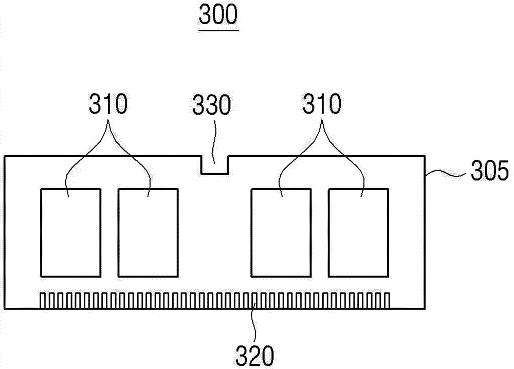
参照图4,存储器模块300可以包括电路板305、包括多个存储器芯片310的存储器部分、端子320、以及连接部分330。Referring to FIG. 4 , the
电路板305是印刷电路板(PCB),在其上安装了诸如多个存储器芯片310之类的部件。电路板305是双面PCB,在两侧都具有导电层。同时,虽然在一个实施例中可以使用双面PCB,但是在其他的实施例中也可以实施在一侧具有导电层的单面PCB。The
电路板305可以具有50mm至60mm的水平长度(特别地,55.2mm),15mm至25mm的垂直长度(特别地,21.8mm),小于0.7mm的厚度(此处,厚度是电路板的厚度)。因为广泛使用的SO-DIMM存储器件典型地具有67.6×30mm的尺寸,所以本发明总构思实施例的存储器模块300在与常规的存储器模块相比时可以具有该典型尺寸减小了40%的尺寸。同时,当存储器模块布置在电路板上时,存储器模块和布置该存储器模块的电路板的厚度可以为3mm至4mm(存储器模块(300)的厚度)。The
存储器部分包括多个存储器芯片310,布置在电路板305上。具体地,多个存储器芯片310可以布置在电路板305的一侧,或布置在电路板305的两侧。可以根据所包括的存储器芯片310的容量和数量以不同方式实现存储器部分的存储容量。例如,如果存储器模块的容量是8Gb,则可以在电路板305的两侧放置并实现8个具有4Gb的存储器芯片。此外,可以在一侧布置4个具有8Gb的存储器芯片,或可以通过在电路板305的每一侧布置2个存储器芯片,来在两侧布置4个具有8Gb的存储器芯片。The memory section includes a plurality of
端子320在电子设备100和多个存储器芯片之间进行接口连接,并布置在电路板305的一侧。具体地,端子320布置在电路板305的该侧上以被安装在主板105的插口210上。图4中示出的示例显示了端子320布置在电路板305的一侧。然而,端子320可以布置在电路板305的不同侧。The terminal 320 interfaces between the
目前广泛使用的SO-DIMM存储器件使用204个端子。然而,考虑到不是所有204端子都被使用,根据本发明总构思的一个实施例,端子320可以具有204个端子,与常规实施方式那样,或具有170至185个端子,使得排除不必要的端子。端子可以以5mm间隔分隔开,如常规的SO-DIMM存储器件那样,或以其他间隔分隔开。具体地,为了减小端子320的总尺寸的长度,端子可以以4mm间隔分隔开。同时,在本实施例中,要说明的是,端子320可以具有170-185个端子,但是端子320也可以具有185-200个端子。The currently widely used SO-DIMM memory device uses 204 terminals. However, considering that not all 204 terminals are used, according to an embodiment of the present general inventive concept, the terminal 320 may have 204 terminals, as in the conventional embodiment, or have 170 to 185 terminals, so that unnecessary terminals are excluded. . The terminals may be spaced at 5 mm intervals, as in conventional SO-DIMM memory devices, or at other intervals. Specifically, in order to reduce the length of the overall size of the terminal 320, the terminals may be spaced apart at intervals of 4 mm. Meanwhile, in this embodiment, it should be noted that the
连接部分330可以布置在电路板305的一侧以面对端子320。具体地,连接部分330可以连接至电子设备100的固定单元220以将存储器模块300固定至电子设备100,并可以设置成如图4所示的具有预定尺寸的槽的形式。连接部分330的位置可以与可附着至电子设备的存储器模块的类型对应,这将在下文中参照图6和图9详细介绍。因为连接部分300被布置在电路板305的仅一侧上,因此与在两侧布置连接部分的常规闩锁(latch)结构相比,连接部分300占据电路板上更少的区域。存储器模块类型可以是DDR3或低功率DD3,但是不限于此。The
根据本发明总构思的一个实施例,存储器模块使用小尺寸的电路板,因而可以以较小的尺寸实现。According to an embodiment of the present general inventive concept, a memory module uses a small-sized circuit board and thus can be implemented in a smaller size.
此外,通过使用形成在电路板的两侧上的闩锁结构和仅在电路板的一侧上设置的连接部分,存储器模块300的尺寸可以显著地减小。Furthermore, the size of the
图5示出根据本发明总构思的第二实施例的存储器模块的电路板。FIG. 5 illustrates a circuit board of a memory module according to a second embodiment of the present general inventive concept.
具体地,根据本发明总构思的第二实施例的存储器模块300’可以包括键销区(key area)350以划分存储器模块类型。Specifically, the memory module 300' according to the second embodiment of the present general inventive concept may include a
参照图5,存储器模块300’可以包括电路板305、包括多个存储器芯片310的存储器部分、端子320、连接部分330以及键销区350。电路板305、包括多个存储器芯片310的存储器部分和连接部分330的构成和操作与根据图4描述的一样,为了简明这里不再进一步介绍。Referring to FIG. 5 , the memory module 300' may include a
端子320包括第一端子321和第二端子322。The terminal 320 includes a
第一端子321包括在电路板305的上表面上以相同间隔分隔开的多个端子。所述多个端子可以以5mm间隔分隔开,与常规的SO-DIMM存储器件的情形一样,或者以4mm间隔分隔开以减小第一端子321的尺寸。The
第二端子包括在电路板305的上表面上以相同间隔分隔开的多个端子。所述多个端子可以以5mm间隔分隔开,与常规的SO-DIMM存储器件的情形一样,或者以4mm间隔分隔开以减小第二端子322的尺寸。The second terminal includes a plurality of terminals spaced at the same interval on the upper surface of the
同时,因为键销区350的位置可以根据存储器件的类型而修改,因而包括在第一端子321内的端子的数量和包括在第二端子322内的端子的数量可以改变。然而,即使如图5所示那样设置键销区350,第一端子321和第二端子322的总端子数量也是相同的,如图4中示出的。具体地,可以设置204个端子,与常规SO-DIMM存储器件的情形相同,或可以设置170至200个端子,使得从204个端子中排除不必要的元件。Meanwhile, since the location of the
如果如图4中示出的那样实现端子320,换句话说,如果不设置键销区350,则第一端子321的端子和第二端子322的相邻端子之间的间隔是与第一(或第二)端子的多个端子之间的间隔相同的间隔。If the terminal 320 is realized as shown in FIG. or second) the intervals between a plurality of terminals of the terminal are the same interval.
键销区350可以形成在第一端子321和第二端子322中。具体地,键销区350可以以预设尺寸的槽的形式实施,并且设置一定位置以便划分存储器模块类型。此外,键销区350可以用于划分安装存储器模块的方向(即,存储器模块的上部/下部位置),因而键销区350可以布置在电路板305的偏移位置(deviated position)处,如图6所示,而不是布置在如图5所示的电路板305一侧的中央处。A
根据本发明总构思的一个实施例,键销区350用于划分存储器模块类型。然而,依据实施例,连接部分330可以执行图5中键销区350的功能。该实施方式将在下文中参照图6详细介绍。According to one embodiment of the present general inventive concept, the
图6示出本发明总构思的第三实施例的存储器模块300”的电路板。FIG. 6 illustrates a circuit board of a
具体地,在根据第三实施例的存储器模块300”中,连接部分330’执行常规的键销区的功能。Specifically, in the
参照图6,存储器模块300”可以包括电路板305、包括多个存储器芯片310的存储器部分、端子320以及连接部分330’。Referring to FIG. 6, a memory module 300'' may include a
连接部分330’布置在电路板305的一侧以面对端子320。具体地,连接部分330’连接至电子设备100的固定单元220以将存储器模块300”固定至电子设备100。连接部分330’的位置可以与可附着至电子设备100的存储器模块的类型对应。同时,连接部分330’可以用于划分安装存储器模块的方向(即,存储器模块的上部/下部位置),并因此连接部分330’可以布置在偏移位置,如图6所示,而不是布置在如图5所示的电路板305一侧的中央处,并且可以根据存储器模块的类型改变连接部分330’的布置。The connection portion 330' is arranged on one side of the
如上所说明的,因为连接部分330’执行常规闩锁结构和键销结构的功能,因而根据本发明总构思的第三实施例的存储器模块的尺寸可以进一步减小。As explained above, the size of the memory module according to the third embodiment of the present general inventive concept can be further reduced because the connection part 330' performs the functions of the conventional latch structure and key pin structure.
图7示出根据本发明总构思的第四实施例的存储器模块的电路板。FIG. 7 illustrates a circuit board of a memory module according to a fourth embodiment of the present general inventive concept.
具体地,根据第四实施例的存储器模块300”’还包括边缘槽306。Specifically, the
参照图7,存储器模块300”’可以包括电路板305、包括多个存储器芯片310的存储器部分、端子320、连接部分330以及边缘槽306。7, the
因为电路板305、包括多个存储器芯片310的存储器部分、端子320以及连接部分330具有与上面参照图4说明相同的构造和操作,为了简明下文不再重复说明。Since the
边缘槽306是对在电子设备100上布置电路板305的方向加以指示的区域。具体地,如图7所示,边缘槽306可以是电路板305的一个顶端(apex)区域(优选地,在形成连接部分330的一侧),其可以实施为被切割为三角形形状(或槽形)。备选地,边缘槽306可以设置在电路板305的与形成连接部分330的一侧不同的一侧上。The
边缘槽306可以应用于根据本发明总构思的每个实施例的存储器模块300。The
图8示出根据本发明总构思的第五实施例的存储器模块的电路板。FIG. 8 illustrates a circuit board of a memory module according to a fifth embodiment of the present general inventive concept.
具体地,根据第五实施例的存储器模块300””还包括屏蔽件340。Specifically, the
参照图8,存储器模块300””可以包括电路板305、包括多个存储器芯片310的存储器部分、端子320、连接部分330以及屏蔽件340。Referring to FIG. 8 , a
因为电路板305、包括多个存储器芯片310的存储器部分、端子320以及连接部分330具有与上面参照图4说明相同的构造和操作,为了简明下文不再重复说明。Since the
屏蔽件340密封电路板305的上部分。具体地,屏蔽件340由金属材料形成并可以布置在存储器芯片310的上部分上以减小存储器模块300””和电子设备100之间的RFI噪声。The
同时,虽然此处示出的本发明总构思的某些实施例描述了屏蔽件340仅布置在电路板305的上部分上,但是备选布置也是可能的。因此,如果存储器芯片310布置在电路板305的两侧,则屏蔽件340也可以布置在电路板305的两侧。Meanwhile, although some embodiments of the present general inventive concept illustrated herein describe that the
此外,虽然本发明总构思的某些实施例描述屏蔽件340仅布置在包括多个存储器芯片310的存储器部分的上部分上,但是备选布置也是可能的。因此,屏蔽件340可以实现为覆盖电路板305的不包括端子320的上表面区域和/或下表面区域的整个区域。Also, although some embodiments of the present general inventive concept describe that the
如上所述,屏蔽件340布置成覆盖存储器模块300””的上部分,因而可以减小存储器模块300””和通信装置之间产生的RFI噪声。As described above, the
图9是说明根据本发明总构思的一个实施例的存储器模块的连接部分的操作的视图。FIG. 9 is a view illustrating an operation of a connection part of a memory module according to one embodiment of the present general inventive concept.
具体地,连接部分330可以执行常规的闩锁结构和键销结构的功能,如上面参照图4和6说明的。例如,如果存储器芯片是DDR3,则连接部分330可以布置在电路板305一侧的中央处。如果存储器芯片是低功率DDR3,则连接部分330’可以布置在电路板305一侧与中央不同的区域处,如图9所示。Specifically, the
图10至12是说明根据本发明总构思的存储器模块300和电子设备100之间的连接部分的操作的视图。10 to 12 are views illustrating operations of a connection portion between the
参照图10,由电子设备100的插口210固定存储器模块300的一侧(在此布置有端子),并且由电子设备100的固定单元220固定存储器模块的另一侧(在此形成有连接部分)。Referring to FIG. 10 , one side of the memory module 300 (where terminals are arranged) is fixed by the
参照图11,存储器模块300的一侧首先固定至电子设备100的插口210,同时存储器模块300关于插口210旋转,存储器模块300的另一侧(更具体地,连接部分330)挤压伞形的紧固(fastening)单元220。当存储器模块挤压伞形紧固单元220时,伞形紧固单元220改变为具有更窄宽度的形状。当伞形紧固单元220的宽度变得更窄时,存储器模块的连接部分330穿过伞形紧固单元220。当连接部分330穿过伞形紧固单元220时,伞形紧固单元220恢复为原始形状,于是将存储器模块300的另一侧固定。11, one side of the
当用户要分离所布置的存储器模块时,通过挤压布置在伞形紧固单元220一侧的杠杆221,伞形紧固单元220的宽度变得更窄,并且存储器模块300和固定单元220可以分离。When the user wants to separate the arranged memory module, by pressing the
同时,虽然图10和11显示了使用伞形紧固装置来实现固定单元220,但是可以使用包括与图10和11中示出的伞形紧固装置不同形状的其他紧固装置来实现固定单元220,只要固定单元220将存储器模块300固定至电子设备100即可。Meanwhile, although FIGS. 10 and 11 show that the fixing
此外,虽然本发明总构思的上述实施例描述了在电子设备100的主板105上可以形成一个存储器模块300,但是在电子设备100的主板105上也可以形成两个存储器模块300,如图12所示。此外,根据本发明总构思的实施例,电子设备100可以具有多于三个安装在其上的存储器模块300。In addition, although the above-mentioned embodiments of the present general inventive concept describe that one
虽然图10至12没有具体示出可以布置在电子设备100的主板105的安装存储器模块300的区域上的其他部件,但是根据本发明总构思的实施例,一般的电子器件,例如电阻器、电容器或晶体管也可以布置在电子设备100的主板105上,或者电子设备100的主板105上也可以包括多个存储器芯片310。因此,存储器部分在电子设备的主板105上占据较少的区域。Although FIGS. 10 to 12 do not specifically show other components that can be arranged on the area where the
虽然已经示出并描述了本发明总构思的若干个实施例,但是本领域技术人员应该认识到,在不脱离本发明总构思的原理和精神的情况下可以对这些实施例作出改变,本发明的范围由权利要求及其等价物限定。Although several embodiments of the general concept of the present invention have been shown and described, those skilled in the art should recognize that changes can be made to these embodiments without departing from the principle and spirit of the general concept of the present invention. The scope is defined by the claims and their equivalents.
Claims (15)
Applications Claiming Priority (4)
| Application Number | Priority Date | Filing Date | Title |
|---|---|---|---|
| KR20120065117 | 2012-06-18 | ||
| KR10-2012-0065117 | 2012-06-18 | ||
| KR10-2013-0044942 | 2013-04-23 | ||
| KR1020130044942A KR20130142065A (en) | 2012-06-18 | 2013-04-23 | Memory apparatus and electronic apparatus |
Publications (1)
| Publication Number | Publication Date |
|---|---|
| CN103517625A true CN103517625A (en) | 2014-01-15 |
Family
ID=48745626
Family Applications (1)
| Application Number | Title | Priority Date | Filing Date |
|---|---|---|---|
| CN201310238021.2A Pending CN103517625A (en) | 2012-06-18 | 2013-06-17 | Memory apparatus and electronic apparatus |
Country Status (3)
| Country | Link |
|---|---|
| US (1) | US20130335909A1 (en) |
| EP (1) | EP2677392A3 (en) |
| CN (1) | CN103517625A (en) |
Cited By (2)
| Publication number | Priority date | Publication date | Assignee | Title |
|---|---|---|---|---|
| CN105720015A (en) * | 2014-12-18 | 2016-06-29 | 英特尔公司 | Cpu package substrates with removable memory mechanical interfaces |
| CN106647956A (en) * | 2015-10-30 | 2017-05-10 | 鸿富锦精密工业(深圳)有限公司 | Connecting component |
Families Citing this family (2)
| Publication number | Priority date | Publication date | Assignee | Title |
|---|---|---|---|---|
| US9288907B2 (en) * | 2014-03-18 | 2016-03-15 | National Chung Shan Institute Of Science And Technology | Microelectronic 3D packaging structure and method of manufacturing the same |
| CN106557130B (en) * | 2015-12-31 | 2023-11-24 | 深圳市嘉合劲威电子科技有限公司 | Memory module and electronic device using same |
Citations (3)
| Publication number | Priority date | Publication date | Assignee | Title |
|---|---|---|---|---|
| US6629855B1 (en) * | 1999-07-01 | 2003-10-07 | Silicon Graphics, Inc. | Memory system including guides that receive memory modules |
| CN1700850A (en) * | 2004-05-20 | 2005-11-23 | 日本电气株式会社 | Semiconductor device, noise reduction method, and shield cover |
| CN1870252A (en) * | 2005-05-27 | 2006-11-29 | 新光电气工业株式会社 | Semiconductor module and semiconductor module heat radiation plate |
Family Cites Families (8)
| Publication number | Priority date | Publication date | Assignee | Title |
|---|---|---|---|---|
| TW394469U (en) * | 1998-12-24 | 2000-06-11 | Foxconn Prec Components Co Ltd | Memory bus module |
| US6362966B1 (en) * | 1999-05-13 | 2002-03-26 | Intel Corporation | Protective cover and packaging for multi-chip memory modules |
| US7234099B2 (en) * | 2003-04-14 | 2007-06-19 | International Business Machines Corporation | High reliability memory module with a fault tolerant address and command bus |
| KR100834826B1 (en) * | 2007-01-25 | 2008-06-03 | 삼성전자주식회사 | Integrated circuit module structure with reduced handling damage and terminal resistor arrangement method |
| TWM393134U (en) * | 2007-03-03 | 2010-11-21 | zhou-xian Cai | Electric connector assembly allowing an interface board moving backward one stroke while inserting |
| US20090111296A1 (en) * | 2007-10-26 | 2009-04-30 | Hon Hai Precision Ind. Co., Ltd. | Latching device used for locking two daughter printed circuit boards in connector set |
| KR101770823B1 (en) * | 2010-03-18 | 2017-08-24 | 삼성전자주식회사 | Large capacity memory module mounting device for portable terminal |
| DE102010032361A1 (en) * | 2010-07-27 | 2012-02-02 | Leopold Kostal Gmbh & Co. Kg | Electrical or electronic device, has multiple bent clamping springs comprising two spring legs, where one of spring legs presses circuit board in interior of housing, and another spring leg forms catch element at outside of housing |
-
2013
- 2013-05-30 US US13/905,218 patent/US20130335909A1/en not_active Abandoned
- 2013-06-11 EP EP13171472.7A patent/EP2677392A3/en not_active Withdrawn
- 2013-06-17 CN CN201310238021.2A patent/CN103517625A/en active Pending
Patent Citations (4)
| Publication number | Priority date | Publication date | Assignee | Title |
|---|---|---|---|---|
| US6629855B1 (en) * | 1999-07-01 | 2003-10-07 | Silicon Graphics, Inc. | Memory system including guides that receive memory modules |
| CN1700850A (en) * | 2004-05-20 | 2005-11-23 | 日本电气株式会社 | Semiconductor device, noise reduction method, and shield cover |
| CN1870252A (en) * | 2005-05-27 | 2006-11-29 | 新光电气工业株式会社 | Semiconductor module and semiconductor module heat radiation plate |
| US7483273B2 (en) * | 2005-05-27 | 2009-01-27 | Shinko Electric Industries Co., Ltd. | Semiconductor module and semiconductor module heat radiation plate |
Cited By (4)
| Publication number | Priority date | Publication date | Assignee | Title |
|---|---|---|---|---|
| CN105720015A (en) * | 2014-12-18 | 2016-06-29 | 英特尔公司 | Cpu package substrates with removable memory mechanical interfaces |
| CN105720015B (en) * | 2014-12-18 | 2019-12-03 | 英特尔公司 | CPU package substrate with mechanical interface for removable memory |
| CN106647956A (en) * | 2015-10-30 | 2017-05-10 | 鸿富锦精密工业(深圳)有限公司 | Connecting component |
| CN106647956B (en) * | 2015-10-30 | 2020-05-19 | 鸿富锦精密电子(天津)有限公司 | Connecting assembly |
Also Published As
| Publication number | Publication date |
|---|---|
| EP2677392A2 (en) | 2013-12-25 |
| EP2677392A3 (en) | 2016-05-04 |
| US20130335909A1 (en) | 2013-12-19 |
Similar Documents
| Publication | Publication Date | Title |
|---|---|---|
| CN113036431B (en) | Foldable electronic devices | |
| US8411458B2 (en) | Apparatus capable of selectively using different types of connectors | |
| CN108431721A (en) | Laptop | |
| CN106207440A (en) | Electronic equipment including antenna device | |
| US10938106B2 (en) | Electronic apparatus | |
| KR102806954B1 (en) | Shielding Member and Electronic Device Including the Same | |
| US20120162016A1 (en) | Antenna module, and touch device and electronic device having the same | |
| CN105529531A (en) | Antenna structures and electronics device having the same | |
| US11369051B2 (en) | Electromagnetic interference (EMI) shielding member and electronic device including the same | |
| JP2007274742A (en) | Combination antenna with many feeder points | |
| CN108879072A (en) | Electronic device | |
| US20070130404A1 (en) | Portable notebook computer motherboard | |
| CN103517625A (en) | Memory apparatus and electronic apparatus | |
| US10522898B2 (en) | Integration of millimeter wave antennas in reduced form factor platforms | |
| US10490909B2 (en) | Antenna device and electronic device including the same | |
| US20090215441A1 (en) | Electronic System | |
| US20140160653A1 (en) | Keyboard configuration for an electronic device | |
| WO2018196692A1 (en) | Card tray assembly, card tray and mobile terminal | |
| CN105514571B (en) | Antenna device and electronic apparatus | |
| CN107623984A (en) | Flexible circuit board, manufacturing method thereof, and electronic device | |
| US12034223B2 (en) | Mobile device with communication and sensing functions | |
| KR20130142065A (en) | Memory apparatus and electronic apparatus | |
| US20150244058A1 (en) | Electronic Device Having Antenna Module | |
| US20110116228A1 (en) | Notebook computer having flexible mounting space for wireless communication module | |
| CN215068014U (en) | PCB substrate, computer mainboard and computer |
Legal Events
| Date | Code | Title | Description |
|---|---|---|---|
| C06 | Publication | ||
| PB01 | Publication | ||
| C10 | Entry into substantive examination | ||
| SE01 | Entry into force of request for substantive examination | ||
| WD01 | Invention patent application deemed withdrawn after publication |
Application publication date: 20140115 |
|
| WD01 | Invention patent application deemed withdrawn after publication |