CN103502945A - Register allocation in rotation based alias protection register - Google Patents
Register allocation in rotation based alias protection register Download PDFInfo
- Publication number
- CN103502945A CN103502945A CN201180070544.XA CN201180070544A CN103502945A CN 103502945 A CN103502945 A CN 103502945A CN 201180070544 A CN201180070544 A CN 201180070544A CN 103502945 A CN103502945 A CN 103502945A
- Authority
- CN
- China
- Prior art keywords
- instruction
- register
- instructions
- alias
- code
- Prior art date
- Legal status (The legal status is an assumption and is not a legal conclusion. Google has not performed a legal analysis and makes no representation as to the accuracy of the status listed.)
- Granted
Links
Images


Classifications
-
- G—PHYSICS
- G06—COMPUTING OR CALCULATING; COUNTING
- G06F—ELECTRIC DIGITAL DATA PROCESSING
- G06F9/00—Arrangements for program control, e.g. control units
- G06F9/06—Arrangements for program control, e.g. control units using stored programs, i.e. using an internal store of processing equipment to receive or retain programs
- G06F9/30—Arrangements for executing machine instructions, e.g. instruction decode
- G06F9/38—Concurrent instruction execution, e.g. pipeline or look ahead
- G06F9/3836—Instruction issuing, e.g. dynamic instruction scheduling or out of order instruction execution
- G06F9/3842—Speculative instruction execution
-
- G—PHYSICS
- G06—COMPUTING OR CALCULATING; COUNTING
- G06F—ELECTRIC DIGITAL DATA PROCESSING
- G06F9/00—Arrangements for program control, e.g. control units
- G06F9/06—Arrangements for program control, e.g. control units using stored programs, i.e. using an internal store of processing equipment to receive or retain programs
- G06F9/30—Arrangements for executing machine instructions, e.g. instruction decode
- G06F9/38—Concurrent instruction execution, e.g. pipeline or look ahead
- G06F9/3824—Operand accessing
- G06F9/3834—Maintaining memory consistency
-
- G—PHYSICS
- G06—COMPUTING OR CALCULATING; COUNTING
- G06F—ELECTRIC DIGITAL DATA PROCESSING
- G06F9/00—Arrangements for program control, e.g. control units
- G06F9/06—Arrangements for program control, e.g. control units using stored programs, i.e. using an internal store of processing equipment to receive or retain programs
- G06F9/30—Arrangements for executing machine instructions, e.g. instruction decode
- G06F9/30098—Register arrangements
- G06F9/3012—Organisation of register space, e.g. banked or distributed register file
- G06F9/3013—Organisation of register space, e.g. banked or distributed register file according to data content, e.g. floating-point registers, address registers
-
- G—PHYSICS
- G06—COMPUTING OR CALCULATING; COUNTING
- G06F—ELECTRIC DIGITAL DATA PROCESSING
- G06F9/00—Arrangements for program control, e.g. control units
- G06F9/06—Arrangements for program control, e.g. control units using stored programs, i.e. using an internal store of processing equipment to receive or retain programs
- G06F9/30—Arrangements for executing machine instructions, e.g. instruction decode
- G06F9/38—Concurrent instruction execution, e.g. pipeline or look ahead
- G06F9/3836—Instruction issuing, e.g. dynamic instruction scheduling or out of order instruction execution
- G06F9/3838—Dependency mechanisms, e.g. register scoreboarding
- G06F9/384—Register renaming
Landscapes
- Engineering & Computer Science (AREA)
- Software Systems (AREA)
- Theoretical Computer Science (AREA)
- Physics & Mathematics (AREA)
- General Engineering & Computer Science (AREA)
- General Physics & Mathematics (AREA)
- Executing Machine-Instructions (AREA)
Abstract
一种系统可以包括优化器/调度器,用于对一组指令进行调度,计算调度的指令组的数据相关性、检查约束和/或防检查约束,以及,基于数据相关性、检查约束和/或防检查约束,为调度的指令组分配别名寄存器。在一个实施例中,优化器用于释放未使用的寄存器,以减少用来保护调度的指令的别名寄存器。优化器进一步将伪指令插入到合并的指令之后,以中断检查约束和防检查约束中的循环。
A system may include an optimizer/scheduler for scheduling a set of instructions, calculating data dependencies, check constraints, and/or anti-check constraints for the scheduled instruction set, and allocating alias registers for the scheduled instruction set based on the data dependencies, check constraints, and/or anti-check constraints. In one embodiment, the optimizer is used to release unused registers to reduce the number of alias registers used to protect the scheduled instructions. The optimizer further inserts pseudo-instructions after the merged instructions to break loops in the check constraints and anti-check constraints.
Description
背景background
硬件/软件共同设计的系统可以利用动态二进制优化来改善性能。对于对存储器指令的动态二进制优化,可能需要存储器别名信息。动态二进制优化可以为原子区中的推测性的存储器优化利用硬件别名检查。当加载指令被推测性地重新排序到存储指令之前并且它们之间有可能的存储器别名时,加载指令可能需要设置别名保护寄存器,其存储器地址存储在其中。响应于存储指令被执行,存储指令可以检查带有其存储器地址的别名保护寄存器来检测错误推测。错误推测可能会导致整个区域的回滚和非优化的或不太优化的代码的重新执行。Hardware/software co-designed systems can take advantage of dynamic binary optimization to improve performance. For dynamic binary optimization of memory instructions, memory alias information may be required. Dynamic binary optimization can take advantage of hardware alias checking for speculative memory optimizations in atomic regions. When a load instruction is speculatively reordered before a store instruction and there is possible memory aliasing between them, the load instruction may need to set an alias protection register, where its memory address is stored. In response to a store instruction being executed, the store instruction may check an alias protection register with its memory address to detect a misspeculation. Misspeculation can lead to rollbacks of entire regions and re-execution of non-optimized or less-optimized code.
附图简述Brief description of the drawings
此处所描述的本发明是作为示例说明的,而不仅限于各个附图的图形。为说明简单和清楚起见,图形中所示出的元件不一定是按比例绘制的。例如,为了清楚起见,某些元件的尺寸可以相对于其他元件而放大。此外,在合适的情况下,在不同的图形中参考标签重复使用,以表示对应的或类似的元件。The invention described herein is by way of illustration and not limited to the figures of the various drawings. For simplicity and clarity of illustration, elements shown in the figures have not necessarily been drawn to scale. For example, the dimensions of some of the elements may be exaggerated relative to other elements for clarity. Further, where appropriate, reference labels have been repeated among the different figures to indicate corresponding or analogous elements.
图1A是根据本发明的一个实施例的示例性系统的框图。Figure 1A is a block diagram of an exemplary system according to one embodiment of the present invention.
图1B是根据本发明的一个实施例的另一示例性系统的框图。Figure IB is a block diagram of another exemplary system according to one embodiment of the present invention.
图1C是根据本发明的一个实施例的再一个示例系统的框图。Figure 1C is a block diagram of yet another example system according to one embodiment of the present invention.
图2A-2K是根据本发明的某些实施例的基于旋转的别名保护寄存器中的寄存器分配的示意图。2A-2K are schematic diagrams of register allocation in rotation-based alias protected registers, according to some embodiments of the invention.
图3是根据本发明的一些实施例的流程图。Figure 3 is a flow diagram according to some embodiments of the invention.
详细描述A detailed description
下面的描述说明了提供别名寄存器分配算法,以减少基于旋转的别名保护寄存器中的寄存器使用的技术。技术的实现不局限在计算系统中;它可以被任何执行环境用于类似的目的,诸如,例如,任何其他数字/电子设备。在下面的描述中,阐述了诸如逻辑实现、操作码、指定操作数的手段、资源分区/共享/重复实现,系统组件的类型和相互关系,以及逻辑分区/集成选择之类的很多具体细节,以便提供对本发明的更全面的理解。然而,本发明可以在没有这样的具体细节的情况下实施。在其他情况下,没有详细示出控制结构和完全软件指令序列,以便不至于使本发明变得模糊。The following description illustrates techniques for providing an alias register allocation algorithm to reduce register usage in rotation-based alias-protected registers. Implementation of the techniques is not limited to computing systems; it can be used for similar purposes by any execution environment, such as, for example, any other digital/electronic device. In the following description, many specific details such as logical implementation, opcodes, means of specifying operands, resource partitioning/sharing/duplication, types and interrelationships of system components, and logical partitioning/integration choices are set forth, in order to provide a more comprehensive understanding of the present invention. However, the invention may be practiced without such specific details. In other instances, control structures and full software instruction sequences have not been shown in detail in order not to obscure the invention.
说明书中对"一个实施例"、"实施例"、"示例实施例"等等的引用表示所描述的实施例可包括特定特征、结构或特性,但是,每一个实施例可以不一定包括该特定特征、结构或特征。此外,这样的短语不一定是指同一个实施例。此外,当结合一个实施例描述特定特征、结构或特性时,认为在本领域技术人员学识范围内,可以与其他实施例一起实施这样的特征、结构或特性,无论是否对此明确描述。References in the specification to "one embodiment," "an embodiment," "example embodiment," etc. mean that the described embodiment may include a particular feature, structure, or characteristic, but that each embodiment may not necessarily include the particular feature, structure, or characteristic. feature, structure or feature. Moreover, such phrases are not necessarily referring to the same embodiment. Furthermore, when a particular feature, structure or characteristic is described in conjunction with one embodiment, it is considered within the purview of those skilled in the art that such feature, structure or characteristic can be implemented with other embodiments whether or not explicitly described therein.
可以使用硬件、软件、固件或其任何组合来实现本发明的各实施例。本发明的各实施例还可实现为存储在机器可读取的介质中的可以由一个或多个处理器读取和执行的指令。机器可读的介质可以包括用于以机器(例如,计算设备)可读的形式存储或传输信息的任何机制。例如,机器可读的介质可以包括,只读存储器(ROM);随机存取存储器(RAM);磁盘存储介质;光存储介质;闪存设备;电的、光学的、声音或其他形式的传播信号(例如,载波、红外信号、数字信号等等);及其他。Embodiments of the invention may be implemented using hardware, software, firmware or any combination thereof. Embodiments of the invention may also be implemented as instructions stored on a machine-readable medium, which may be read and executed by one or more processors. A machine-readable medium may include any mechanism for storing or transmitting information in a form readable by a machine (eg, a computing device). For example, a machine-readable medium may include, read-only memory (ROM); random-access memory (RAM); magnetic disk storage media; optical storage media; flash memory devices; electrical, optical, acoustic, or other forms of propagated signals ( For example, carrier waves, infrared signals, digital signals, etc.); and others.
下面的描述可以包括只用于描述性的目的而不应该理解为限制性的诸如第一、第二等等之类的术语。The following description may include terms such as first, second, etc., which are used for descriptive purposes only and should not be construed as limiting.
图1A示出了系统100的示例性实施例的框图。系统100可以包括处理器102。处理器102可以包括任何类型的能够执行软件和/或处理数据信号的处理器。在一个实施例中,处理器102可以包括复杂指令集计算机(CISC)微处理器、精简指令集计算(RISC)微处理器、超长指令字(VLIW)微处理器、实现指令集的组合的处理器,或任何其他处理器设备,诸如数字信号处理器,诸如微处理器、数字信号处理器或微控制器。FIG. 1A shows a block diagram of an exemplary embodiment of a
虽然图1A只示出了一个这样的处理器102,但是,系统100中可以有一个或多个处理器,一个或多个处理器可以包括多个线程、多个核等等。本增强不仅限于计算系统。本发明的替换实施例可以用于使用统一可扩展固件接口(UEFI)基本输入/输出系统(BIOS)的诸如手持式设备和嵌入式应用之类的任何形状因子设备中。手持式设备的某些示例包括蜂窝电话、网际协议设备、数码相机、个人数字助理(PDA),或诸如上网本或笔记本之类的手持式PC。嵌入式应用可包括微控制器、数字信号处理器(DSP)、单片系统、网络计算机(NetPC)、机顶盒、网络中枢、广域网(WAN)交换机,或任何其他系统。Although only one
处理器102可以耦合到系统逻辑芯片104。例如,在所示出的实施例中,系统逻辑芯片104可以是存储器控制器中枢(MCH)。在一个实施例中,MCH104可以提供到系统存储器106的存储器路径120用于指令和数据存储和/或用于例如图形命令、数据和纹理的存储。存储器路径120可以包括存储器总线。MCH104可以在系统100中的处理器102、系统存储器106、及其他组件之间定向数据信号,并在处理器102、系统存储器106、以及系统I/O之间桥接数据信号。存储器106可以是硬盘、软盘、随机存取存储器(RAM)、只读存储器(ROM)、闪存,或可由处理器102读取的任何其他类型的介质。
MCH104可以通过本地I/O互连来耦合到I/O控制器中枢(ICH)108。在一个实施例中,本地I/O互连可以是诸如外围组件互连(PCI)总线之类的高速I/O总线。ICH108可以,例如,通过本地I/O互连,提供到一个或多个I/O设备的连接。某些示例可以包括数据存储设备118、音频I/O120、键盘/鼠标I/O122,以及网络控制器116,或其他集成的I/O组件,诸如集成的驱动器电子设备(IDE),局域网(LAN)和串行扩展端口,诸如通用串行总线(USB)、PCI插槽(未示出)、无线收发器,旧式I/O控制器等等。数据存储设备118可以包括硬盘驱动器、软盘驱动器、CD-ROM设备、闪存设备,或其他大容量存储设备。
参考图1A,诸如闪存112之类的非易失性存储器可以通过,例如,低管脚数(LPC)总线,耦合到ICH108。BIOS固件114可以驻留在闪存112中,引导程序可以执行来自闪存,或固件的指令。虽然图1A示出了闪存112中的BIOS固件114,但是,在某些实施例中,BIOS固件114可以存储在诸如固件中枢之类的其他非易失性存储器等等中。在一个实施例中,BIOS固件114可以通过统一可扩展固件接口(UEFI)固件或任何其他固件来实现。Referring to FIG. 1A , non-volatile memory such as flash memory 112 may be coupled to ICH 108 via, for example, a low pin count (LPC) bus.
虽然图1A示出了系统100,但是,根据本发明的各实施例可以用于任何其他硬件体系结构中,诸如使用多个处理器核的平台,或使用处理器或协同处理器的平台,使用I/O中枢的平台,或可以使用嵌入在处理器内的存储器控制等等。Although FIG. 1A shows
图1B示出了实现本发明的原理的系统140的替换实施例。系统140可以包括处理器142。处理器142可以包括任何类型的能够执行软件和/或处理数据信号的处理器。在一个实施例中,处理器142可以包括如上文对于处理器102所提及的任何类型的处理器或处理器设备。在一个实施例中,处理器142可以通过存储器路径(未示出)耦合到用于指令和数据存储和/或用于,例如,图形命令、数据和纹理的存储的系统存储器144。在另一个实施例中,处理器142可以通过PCI互连耦合到一个或多个外围组件互连(PCI)端口160;然而,在某些实施例中,PCI端口160可能不是必需的。存储器144可以是硬盘、软盘、随机存取存储器(RAM)、只读存储器(ROM)、闪存,或可由处理器142读取的任何其他类型的介质。Figure IB illustrates an alternate embodiment of a
虽然图1B只示出了一个这样的处理器142,但是,系统140中可以有一个或多个处理器,一个或多个处理器可以包括多个线程、多个核等等。本增强不仅限于计算机系统或数据处理设备系统。本发明的替换实施例可以用于使用统一可扩展固件接口(UEFI)基本输入/输出系统(BIOS)的诸如手持式设备和嵌入式应用之类的任何形状因子设备中。手持式设备的某些示例包括蜂窝电话、网际协议设备、数码相机、个人数字助理(PDA),或诸如上网本或笔记本之类的手持式PC,或诸如平板电脑或智能电话之类的智能设备等等。嵌入式应用可包括微控制器、数字信号处理器(DSP)、单片系统、网络计算机(NetPC)、机顶盒、网络中枢、广域网(WAN)交换机,或任何其他系统。Although FIG. 1B shows only one
处理器142可以耦合到系统逻辑芯片146。例如,在所示出的实施例中,系统逻辑芯片146可以是平台控制器中枢(PCH)。在一个实施例中,PCH146可以,例如,通过本地I/O互连,提供到一个或多个I/O设备的连接。在一个实施例中,本地I/O互连可以是诸如外围组件互连(PCI)总线之类的高速I/O总线。PCH146可以在处理器142和系统140中的一个或多个其他组件之间定向数据信号或其他信息,并在处理器142和系统I/O之间桥接数据信号或信息。
一个或多个组件的某些示例可以包括数据存储设备142、一个或多个PCI端口154、网络控制156、USB端口158。在一个实施例中、数据存储设备152可以包括硬盘驱动器、软盘驱动器、CD-ROM设备、闪存设备,或其他大容量存储设备。虽然图1B示出了组件的某些示例,但是PCH146可以提供到任何其他组件的连接,诸如音频I/O、键盘/鼠标I/O,及其他集成I/O组件,诸如集成的驱动器电子设备(IDE)、局域网(LAN)及其他串行扩展端口,无线收发器,旧式I/O控制器等等。Some examples of one or more components may include
参考图1B,诸如闪存148之类的非易失性存储器可以通过,例如,低管脚数(LPC)总线,耦合到PCH146。BIOS固件150可以驻留在闪存148中,引导程序可以执行来自闪存或固件的指令。虽然图1B示出了闪存148中的BIOS固件150,但是,在某些实施例中,BIOS固件150可以存储在诸如固件中枢之类的其他非易失性存储器等等中。在一个实施例中,BIOS固件150可以通过统一可扩展固件接口(UEFI)固件或任何其他固件来实现。Referring to FIG. 1B , non-volatile memory such as flash memory 148 may be coupled to
虽然图1B示出了系统140,但是,根据本发明的各实施例可以用于任何其他硬件和软件体系结构中,诸如使用多个处理器核的平台,或使用处理器或协同处理器的平台,使用I/O集线器的平台,或可以使用嵌入在处理器内的存储器控制等等。Although FIG. 1B shows
图1C示出了可以实现本发明的原理的系统160的另一实施例。系统160可以包括处理器162。处理器162可以包括任何类型的能够执行软件和/或处理数据信号的处理器。处理器162可以包括如上文对于处理器102所提及的任何类型的处理器或处理器设备。系统160可以包括存储器163,该存储器163可以通过互连168或诸如总线、存储器路径等等之类的任何其他连接耦合到处理器162。存储器163的示例可以包括硬盘、软盘、随机存取存储器(RAM)、只读存储器(ROM)、闪存、易失性存储器设备或非易失性存储器设备,或任何其他类型的可由处理器162读取的介质。在另一个实施例中,处理器162可以耦合到网络组件164,网络组件164可以包括,例如,有线网络连接和/或无线网络连接或任何其他网络连接。处理器162可以进一步耦合到I/O控制器165,该I/O控制器165可以耦合到一个或多个I/O设备166。图1C示出了系统160的实施例;在某些实施例中,系统160可以包括可以以硬件、软件、固件或它们的任何组合来实现的一个或多个其他组件。在另一个实施例中,系统160的示例可以包括如上文对于图1A或1B所提及的任何形状因子设备或装置。Figure 1C illustrates another embodiment of a
图2A是根据本发明的一个实施例的示意图。参考编号210可以表示可以具有store_0(存储_0)、store_1等等的顺序的原始代码或指令,如图2A所示。在一个实施例中,原始代码可以在原子区内;然而,在某些实施例中,原子区可能不是必需的。在一个实施例中,可以将原始代码210重新排序或调度到可以相对于原始代码具有不同的序列或顺序的调度的代码或指令220。例如,指令220a可以表示存储器存储指令store_5,该存储器存储指令store_5可以被调度到由,例如,执行逻辑执行的第一指令。图2A的实施例可以使用基于旋转的别名保护寄存器,这些寄存器可以允许每一个存储器指令设置别名保护寄存器,并针对带有比特屏蔽的一组别名保护寄存器进行检查。Figure 2A is a schematic diagram according to one embodiment of the present invention.
在一个实施例中,可以使用基于旋转的别名检查。别名保护寄存器可以以环形缓存器或基于AHPTR(别名首部指示符)270旋转的循环队列来组织,AHPTR270可以指向环形缓存器的首部。存储器指令可以指定相对于当前AHPTR270的别名保护寄存器编号ORD230(带有可能的折回)。例如,参考图2A,基于原始代码的顺序,可以在环形缓存器的首部设置第一指令store_0的带有寄存器ORD“0”的第一别名保护寄存器,第二指令store_1可以指定带有寄存器ORD“1”的第二别名保护寄存器,等等。在另一个实施例中,存储器指令可以具有P比特以表示,诸如处理器102或142之类的硬件或任何其他执行逻辑可以为当前指令设置带有寄存器编号AHPTR+ORD的别名保护寄存器。在一个实施例中,可以检查[AHPTR+ORD,AHPTR)的范围中的寄存器。例如,如果AHPTR=2,ORD=1,并且总的寄存器编号是5(例如,0-4),则可以检查[3,2)范围内的寄存器3,寄存器4,寄存器0和寄存器1。在一个实施例中,可以使用折回。In one embodiment, rotation based alias checking may be used. Alias protection registers can be organized as ring buffers or circular queues that rotate based on AHPTR (Alias Header Indicator) 270, which can point to the head of the ring buffer. A memory instruction may specify an alias protected register number ORD230 relative to the current AHPTR270 (with possible wraparound). For example, referring to FIG. 2A , based on the sequence of the original code, the first alias protection register with register ORD "0" of the first instruction store_0 may be set at the head of the ring buffer, and the second instruction store_1 may specify a register with register ORD " 1" for the second alias protection register, and so on. In another embodiment, a memory instruction may have a P bit to indicate that hardware such as
存储器指令可以具有C比特以表示,诸如处理器之类的硬件或任何其他执行逻辑可以检查所有带有寄存器编号>=AHPTR+ORD(带有可能的折回)的别名保护寄存器。响应于指令调度,可以基于指令的原始执行顺序,为调度的指令分配带有编号ORD230的别名保护寄存器。例如,在图2A中,作为原始程序执行的顺序,可以分配带有ORD230的别名保护寄存器。Memory instructions can have a C bit to indicate that hardware such as a processor or any other execution logic can check all alias protected registers with register numbers >= AHPTR+ORD (with possible wrapping). In response to instruction scheduling, an alias protection register with number ORD230 may be assigned to the scheduled instruction based on the original order of execution of the instructions. For example, in FIG. 2A, an alias protection register with ORD230 may be allocated as the order of original program execution.
在另一个实施例中,存储器指令可以指定旋转编号ROT,该ROT可以表示别名首部指示符可以旋转ROT中所指出的量。在一个实施例中,可以使用旋转值ROT来表示可以释放AHPTR和AHPTR+ROT之间的所有别名保护寄存器(带有可能的折回,包括AHPTR,排除AHPTR+ROT),例如,在执行指令之前。在一个实施例中,诸如处理器102或142之类的硬件可以将AHPTR旋转ROT,并清除AHPTR和AHPTR+ROT之间的别名保护寄存器的所有有效比特。In another embodiment, the memory instruction may specify a rotation number ROT, which may indicate that the alias header indicator may be rotated by the amount indicated in the ROT. In one embodiment, a rotation value ROT may be used to indicate that all alias protection registers between AHPTR and AHPTR+ROT (with possible wraparound, including AHPTR, excluding AHPTR+ROT) may be released, e.g., before an instruction is executed. In one embodiment, hardware such as
在一个实施例中,响应于设置带有P比特的别名保护寄存器,硬件可以为寄存器设置有效比特。例如,带有,例如,逻辑“1”的有效比特可以表示可以通过,例如,硬件,检查的有效别名保护寄存器。在另一个实施例中,带有逻辑值,例如,“0”的有效比特可以表示可以不检查相应的别名保护寄存器。例如,图2A的数字参考编号240可以表示“valid_all(有效_全部)”,“valid_all”可以包括一组一个或多个别名保护寄存器的一组一个或多个有效比特。在一个实施例中,“valid_all”240中的有效比特的数量可以与别名保护寄存器的数量和/或调度的指令的数量相同;然而,在某些实施例中,有效比特的数量可以不同于调度的指令的数量。例如,基于原始代码的顺序,可以在valid_all240的最高阶比特设置最后一个指令store_5的带有ORD“5”的别名保护寄存器的有效比特,并可以在valid_all240的最低阶比特设置第一指令store_0的带有ORD“0”的别名保护寄存器的有效比特,等等;然而,在某些实施例中,可以按不同的顺序提供valid_all240中的有效比特。在某些实施例中,valid_all240中的有效比特可以具有基于别名保护寄存器的ORD的顺序。In one embodiment, hardware may set the valid bit for the register in response to setting the alias protection register with the P bit. For example, a valid bit with, for example, a logical "1" may indicate a valid alias protection register that may be checked by, for example, hardware. In another embodiment, a valid bit with a logical value, eg, "0" may indicate that the corresponding alias protection register may not be checked. For example,
例如,valid_all字段240a可以是“000000”,“000000”可以表示对于指令“store_5”(调度的序列中的第一指令),可以不检查别名保护寄存器中的任何一个。valid_all字段240b可以涉及调度的代码中的后续指令“store_2”。valid_all字段240b可以是“100000”,其中,有效比特“1”可以对应于前一指令“store_5”,并可以表示可以检查“store_5”的别名保护寄存器。而且,240b中的有效比特“00000”可以表示,可以不检查store_2其本身、store_0、load_4(加载_4)、store_1,load_3的别名保护寄存器。For example, valid_all field 240a may be "000000", which may indicate that for instruction "store_5" (the first instruction in the dispatched sequence), none of the alias protection registers may be checked. The valid_all field 240b may refer to the subsequent instruction "store_2" in the dispatched code. The valid_all field 240b may be "100000", where the valid bit "1" may correspond to the previous instruction "store_5" and may indicate that the alias protection register of "store_5" may be checked. Moreover, the valid bit "00000" in 240b may indicate that the alias protection registers of store_2 itself, store_0, load_4 (load_4), store_1, and load_3 may not be checked.
参考图2A,valid_st(有效_st)字段250可以涉及存储指令,并可以包括一组一个或多个有效比特。例如,valid_st250可以与valid_all240的不同之处在于,加载指令的别名保护寄存器的有效比特可以具有valid_st250中的逻辑值“0”。在一个实施例中,诸如102或142之类的硬件或其他执行逻辑可以为,例如,所有别名保护寄存器维持有效比特,并在执行每一个指令之前,计算比特屏蔽260,用于检查。加载指令可以不检查另一个加载指令。从load_3的比特屏蔽260a可以看出,可以没有load_4的有效比特(例如,逻辑值“1”),或可以不断言load_4的别名保护寄存器的有效比特。在另一个实施例中,对于load_3的比特屏蔽260a,可以没有按原始执行顺序排序在load_3之前的store_0,store_1,和store_2的有效比特。硬件可以为所有指令(例如,valid_all240)以及只为存储指令(例如,valid_st250),维持单独的有效比特。存储指令可以检查valid_all240,加载指令可以只检查valid_st250。Referring to FIG. 2A , valid_st (valid_st)
图2A示出了诸如处理器或任何其他执行逻辑之类的硬件维持valid_all240、valid_st250并基于ORD230,例如,以C语言语义,计算屏蔽260的公式的实施例。图2A的基于旋转的别名保护寄存器的寄存器分配的算法可以按它们的原始程序顺序为每一个指令分配寄存器,在图2A中示为“寄存器ORD”230。可以使用该算法来保证在别名检查中没有假阴性或假阳性。参考图2A,在一个实施例中,每一个指令都可以具有P/C比特(未示出),但是可以不具有ROT。在再一个实施例中,诸如处理器或任何其他执行逻辑之类的硬件可以运行带有ORD/P/C230的调度的代码220,并计算valid_all240、valid_st250和valid_mask(有效_屏蔽)260,以执行别名检查。FIG. 2A shows an embodiment where hardware, such as a processor or any other executing logic, maintains
参考图2B,示出了寄存器分配的实施例。在一个实施例中,可以使用图2B的寄存器分配来减少基于旋转的别名保护寄存器方案中所使用的别名保护寄存器的数量,并可能不生成假阳性或假阴性。图2B的实施例可以与指令调度和优化集成,并可以用于动态优化。在一个实施例中,不是每一个存储器指令都可以设置别名保护寄存器,并且不是每一个存储器指令都可以检查其他别名保护寄存器。例如,在图2B中,store_0、store_1和load_3中一个也不可以设置别名保护寄存器,因为没有指令可以检查它们。Store_5可以不检查任何其他别名保护寄存器,因为它被调度为区域中的第一指令。图2B的实施例可以使用三个寄存器,而并非六个寄存器。Referring to FIG. 2B, an embodiment of register allocation is shown. In one embodiment, the register allocation of FIG. 2B may be used to reduce the number of alias guard registers used in a rotation-based alias guard register scheme and possibly not generate false positives or false negatives. The embodiment of Figure 2B can be integrated with instruction scheduling and optimization, and can be used for dynamic optimization. In one embodiment, not every memory instruction may set an alias protection register, and not every memory instruction may check other alias protection registers. For example, in FIG. 2B, none of store_0, store_1, and load_3 can also set the alias protection register, because no instruction can check them. Store_5 may not check any other alias protection registers because it is dispatched as the first instruction in the region. The embodiment of Figure 2B can use three registers instead of six.
参考图2B,store_5、store_2和load_4可能需要保护(例如,它们的P比特可以设置为1,它们的C比特(未示出)可以设置为0),可以给它们分别分配带有ORD编号2,0,和1的寄存器。Store_0、store_1和load_3可能不需要保护,并可能只检查其他别名寄存器(例如,它们的P比特可以设置为0,它们的C比特可以设置为1)。图2B示出了基于ORD,P和C计算valid_all240、valid_st250和屏蔽260的实施例。Referring to Figure 2B, store_5, store_2 and load_4 may need to be protected (for example, their P bit may be set to 1, their C bit (not shown) may be set to 0), and they may be assigned with
图2C示出了寄存器分配的另一实施例。在图2C的实施例中,响应于判断store_1和load_4可以不访问同一个存储器,例如,通过软件分析,store_1可以不检查load_4。图2C的实施例可以使用两个寄存器。参考图2C,可以保护store_5、store_2(例如,它们的P比特=1),可以给它们分别分配带有ORD1,以及0的寄存器。store_0,load_4,store_1以及load_3(例如,它们的P比特=0,C比特=1)可以只检查其他别名寄存器。在图2A到2C的各实施例中,寄存器分配可以遵循原始程序顺序。例如,如果在原始程序中第一指令将在第二指令之前执行,则第一指令的寄存器编号可以不大于第二指令。Figure 2C shows another embodiment of register allocation. In the embodiment of FIG. 2C , in response to determining that store_1 and load_4 may not access the same memory, for example, store_1 may not check load_4 through software analysis. The embodiment of Figure 2C can use two registers. Referring to FIG. 2C , store_5 and store_2 can be protected (for example, their P bits=1), and registers with ORD1 and 0 can be assigned to them, respectively. store_0, load_4, store_1 and load_3 (eg, their P bit = 0, C bit = 1) can just check other alias registers. In the various embodiments of Figures 2A-2C, register allocation may follow the original program order. For example, if a first instruction is to be executed before a second instruction in the original program, the register number of the first instruction may not be greater than that of the second instruction.
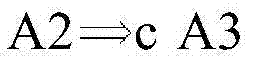
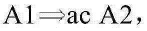
图2D示出了寄存器分配的再一个实施例。参考图2D,示出了数据相关性的实施例。例如,可以定义相关性A1→A2,如果1)以原始程序顺序,指令A1将在指令A2之前执行;2)A1和A2可以访问同一个存储器;3)A1和A2中的至少一个是存储指令。图2D进一步示出了检查约束的实施例。例如,响应于,例如,指令调度器推测A1和A2在运行时可能不会冲突,指令调度器可以将A2移动到A1之前。例如,指令调度器可以通过软件来实现。如果A1→A2,并且指令A2被重新排序到A1之前,则A2可以设置要由A1检查的别名保护寄存器。可以定义检查约束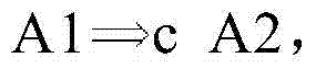
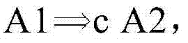
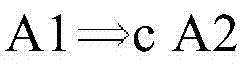
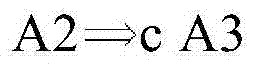

在一个实施例中,检查约束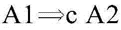
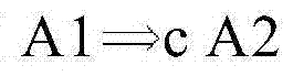
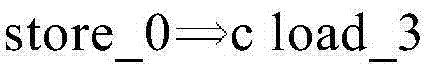
图2E示出了不在原始程序顺序里的寄存器分配的实施例。例如,参考图2E,可以按与它们的原始程序顺序相反的顺序,分别将寄存器0和1分配给load_3和load_1。参考图2E,Load_3的寄存器0(ORD0/P)可以只由Store_2检查(ORD0/C)。在图2E的实施例中,在Store_2之后,可以不检查寄存器0。参考图2F,可以旋转AHPTR达ROT“1”,以释放寄存器0。例如,寄存器0可以在load_1的执行开始时旋转和释放;然而,在某些实施例中,寄存器0可以被释放,例如,响应于寄存器可能已经被检查并可能不被任何其他指令使用。在另一个实施例中,旋转可以在store_2的执行之后执行。响应于旋转,AHPTR可以增大1(例如,当前AHPTR=1)。对于相对于当前AHPTR计数的后续指令,ORD仍可以是“0”。图2E和图2F可以执行相同别名检查。例如,图2F可以利用旋转将寄存器编号减少为1个寄存器。Figure 2E shows an embodiment of register allocation that is not in original program order. For example, referring to FIG. 2E, registers 0 and 1 may be assigned to load_3 and load_1, respectively, in reverse order to their original program order. Referring to FIG. 2E, Register 0 (ORD0/P) of Load_3 can only be checked by Store_2 (ORD0/C). In the embodiment of FIG. 2E, register 0 may not be checked after Store_2. Referring to Figure 2F, AHPTR can be rotated by ROT "1" to release
在图2F的利用旋转的寄存器分配的实施例中,可以响应于store_2已经检查寄存器0,load_3所使用的寄存器0通过寄存器旋转来释放。在此实施例中,可以使用一个寄存器。图2F示出了基于ORD,P,C,ROT和寄存器计数REG(例如,1)来计算valid_all、valid_st和屏蔽的实施例。在一个实施例中,可以相对于AHPTR,计算公式中的valid_all、valid_st和屏蔽。例如:In the embodiment of register allocation with rotation of FIG. 2F , register 0 used by load_3 may be freed by register rotation in response to store_2 having checked
mask(n)=valid_all(n)&~((1<<ORD(n))-1),如果n是存储且C(n);mask(n)=valid_all(n)&~((1<<ORD(n))-1), if n is stored and C(n);
=valid_st(n)&~((1<<ORD(n))-1),如果n是加载且C(n).=valid_st(n)&~((1<<ORD(n))-1), if n is loaded and C(n).
在一个实施例中,硬件可以循环地将屏蔽左移位,达AHPTR,以便检查。在一个实施例中,“循环地左移位”可以将屏蔽中的比特向左移,并向右折回溢出比特。例如,对于屏蔽00001111,循环地左移位2,会导致00111100。在图2F的实施例中,可以相对于AHPTR,计算valid_all、valid_st,以及屏蔽。例如,如果AHPTR=2,屏蔽00001111可以表示寄存器2到寄存器5具有屏蔽值“1”,寄存器6、7、0、1中每一个都可以具有屏蔽值“0”。In one embodiment, the hardware may cyclically left-shift the mask by AHPTR for inspection. In one embodiment, "cyclically left shift" may shift the bits in the mask to the left and fold back the overflow bits to the right. For example, for a mask of 00001111, a circular left shift of 2 results in 00111100. In the embodiment of FIG. 2F, valid_all, valid_st, and mask can be calculated relative to AHPTR. For example, if AHPTR=2, a mask of 00001111 may indicate that registers 2 through 5 have a mask value of "1," and registers 6, 7, 0, and 1 may each have a mask value of "0."
可以使用图2G的实施例来基于与指令调度集成的检查约束和防检查约束来提供寄存器分配。在一个实施例中,如果
在一个实施例中,基于防检查约束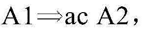
当用完别名寄存器时,可以使用图2G的实施例来动态地限制调度。参考图2G,可以在调度过程中递增地构建检查约束和防检查约束。可以只响应于指令被调度,分配指令的寄存器。如果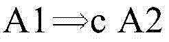
参考图2G,可以与指令调度集成的寄存器分配的实施例。在一个实施例中,实施例可以检查它是否用完寄存器(例如,ORD(A)>=REG)。参考图2G,ORD(A)可以涉及三个变量,可以表示寄存器计数的REG、AHPTR和AHPTR_AT(A)。AHPTR可以始终可用。变量“REG”可以被若干个指令包围,P(A)=1和!R(A),P(A)可以表示指令A可能需要新寄存器来设置保护,!R(A)可以表示指令A的寄存器还没有分配。例如,变量“REG”可以被其寄存器分配被延迟的若干个指令包围。在一个实施例中,AHPTR可以保持按调度的顺序增大。AHPTR_AT(A)可以为延迟的寄存器分配,在执行指令A时记录AHPTR。在一个实施例中,可以计数延迟的寄存器分配,以阻止寄存器溢出。Referring to Figure 2G, an embodiment of register allocation that can be integrated with instruction scheduling. In one embodiment, an embodiment may check if it is out of registers (eg, ORD(A)>=REG). Referring to FIG. 2G, ORD(A) may refer to three variables, REG, AHPTR, and AHPTR_AT(A), which may represent register counts. AHPTR can always be used. The variable "REG" can be surrounded by several instructions, P(A)=1 and !R(A), P(A) can indicate that instruction A may need a new register to set protection, and !R(A) can indicate that instruction A's Registers are not allocated yet. For example, a variable "REG" may be surrounded by several instructions whose register allocations are delayed. In one embodiment, AHPTR may keep increasing in a scheduled order. AHPTR_AT(A) can be allocated for delayed registers, and AHPTR is recorded when instruction A is executed. In one embodiment, delayed register allocations can be counted to prevent register overflow.
在一个实施例中,优化器/调度器可以在调度过程中跟踪诸如变量REG、AHPTR,AHPTR_AT之类的信息,以估计是否有一个或多个别名保护寄存器待被分配给调度的指令或它是否用完寄存器。在一个实施例中,响应于用完寄存器,可以防止任何新指令A的重新排序(即,P(A)=1)。在一个实施例中,可以按它们的原始执行顺序来调度剩余指令,以避免重新排序。In one embodiment, the optimizer/scheduler can track information such as the variables REG, AHPTR, AHPTR_AT during the scheduling process to estimate whether there are one or more alias protection registers to be assigned to the scheduled instruction or whether it Running out of registers. In one embodiment, in response to running out of registers, reordering of any new instructions A may be prevented (ie, P(A)=1). In one embodiment, the remaining instructions may be scheduled in their original order of execution to avoid reordering.
图2H示出了可以使用别名寄存器的处理存储器优化的实施例。如果第二存储器操作可能与它们之间的某些存储器操作有冲突,则优化可能是推测性的。例如,推测性的存储器优化可以使用别名寄存器保护和检查。可以在指令调度之前应用优化,可以在指令调度过程中执行别名寄存器分配:然而,在某些实施例中,指令优化可能不是必需的。响应于优化和在调度过程中,已优化的代码可以在逻辑上被视为将消除的指令合并到其他指令,而合并的指令/代码可以用于所有消除的指令上的别名检查。参考图2H,在store-load(存储-加载)消除282的实施例中,代码可以在逻辑上被视为将load_2合并到store_1。在load-load(加载-加载)消除284,代码可以在逻辑上被视为将load_2合并到load_1。在store-store-elimination(存储-存储-消除)286,代码可以在逻辑上被视为将store_1合并到store_2。在一个实施例中,合并的指令可以包含一个或多个逻辑指令/代码。Figure 2H illustrates an embodiment of processing memory optimization that may use alias registers. Optimizations may be speculative if the second memory operation may conflict with some memory operations between them. For example, speculative memory optimizations can use alias register protection and checking. Optimizations may be applied prior to instruction dispatch, and alias register allocation may be performed during instruction dispatch: however, in some embodiments, instruction optimization may not be necessary. In response to optimization and during scheduling, optimized code can be logically viewed as merging eliminated instructions into other instructions, and the merged instruction/code can be used for alias checking on all eliminated instructions. Referring to FIG. 2H , in an embodiment of store-
在对于合并的指令的调度过程中,可以考虑合并的指令中的逻辑指令上的约束。例如,在图2I所示的代码中,可以从store_0到load_3应用store-load-elimination(存储-加载-消除)。在优化之后以及在调度中,当调度store_0时,可以考虑store_0和load_3上的约束。在图2I中,示出了寄存器分配。参考图2I,在优化中,Store_2可以检查Load_3,Store_0可以检查Load_1。响应于Load_3和Store_0被合并到Store_0,Store_2可以检查Store_0,Store_0可以检查Load_1。Store_0和Load_1可能需要保护(P比特=1),并可以被分配寄存器0,1。Store_2和Store_0可以对照寄存器0检查(C比特=1)。Store_0可以在设置保护(P比特=1)之前检查寄存器0,如此,Store_0可以不检查其本身。During the scheduling process for the merged instructions, constraints on the logical instructions in the merged instructions may be considered. For example, in the code shown in Figure 2I, store-load-elimination can be applied from store_0 to load_3. After optimization as well as in scheduling, constraints on store_0 and load_3 can be considered when scheduling store_0. In Figure 2I, the register allocation is shown. Referring to FIG. 2I, in optimization, Store_2 can check Load_3, and Store_0 can check Load_1. In response to Load_3 and Store_0 being merged into Store_0, Store_2 may check Store_0, and Store_0 may check Load_1. Store_0 and Load_1 may need to be protected (P bit = 1) and can be assigned
在某些实施例中,合并的指令可能在数据相关性中包含循环,这可能会导致检查/防检查约束中的循环。例如,检查/防检查约束中的循环可以被表示为:
图2J示出了插入伪加载以中断约束循环的实施例。参考2J,在一个实施例中,合并的指令可以使用一个或多个别名保护寄存器来中断约束循环。在另一个实施例中,可以将可以与合并的指令访问同一个存储器但是相对于合并的指令可以使用不同的别名保护寄存器的伪存储器指令插入在合并的指令紧接的后面。在一个实施例中,硬件可以实现伪存储器指令,以只执行别名保护/检查,而没有实际存储器访问,以减少开销。Figure 2J shows an embodiment where a dummy load is inserted to break a constrained loop. Referring to 2J, in one embodiment, merged instructions may use one or more alias guard registers to break constrained loops. In another embodiment, a dummy memory instruction that can access the same memory as the merged instruction but can use a different alias protection register than the merged instruction can be inserted immediately after the merged instruction. In one embodiment, hardware may implement dummy memory instructions to only perform alias protection/checking without actual memory accesses to reduce overhead.
在一个实施例中,如果约束循环可能不频繁地发生,当约束循环即将发生时,可以插入伪存储器操作。例如,在调度过程中,可以跟踪有关合并的指令中的每一个逻辑指令的P/C比特的信息。在P/C比特位于合并的指令中的一个或多个逻辑指令的情况下,可以插入伪存储器指令以分区P/C比特。在某些实施例中,如果合并的指令中的一个或多个逻辑指令访问同一个存储器,则可以避免合并的指令中的一个或多个逻辑指令上的P/C比特设置。例如,在图2H所示的加载-加载消除情况下,响应于Load_2检查的指令可以始终由Load_1检查,Load_2上的C比特可以不设置。类似地,响应于检查Load_1的指令可以始终检查Load_2,Load_1上的P比特可以不设置。在一个实施例中,可以保留至多三个逻辑指令上的C/P比特,诸如带有C比特的最早的指令,带有P比特的最近的指令和带有P比特的最近的存储,不管有多少逻辑指令被合并到合并的指令中。图2J的实施例示出了使用伪存储器指令来中断循环的示例。In one embodiment, if a bound loop is likely to occur infrequently, a dummy memory operation may be inserted when a bound loop is about to occur. For example, during scheduling, information about the P/C bit of each logical instruction in the merged instructions may be tracked. In cases where the P/C bit is located in one or more logical instructions within the merged instruction, a dummy memory instruction may be inserted to partition the P/C bit. In some embodiments, a P/C bit setting on one or more of the logical instructions in the merged instruction may be avoided if the one or more logical instructions in the merged instruction access the same memory. For example, in the load-load-elimination case shown in Figure 2H, an instruction that responds to Load_2 checks may always be checked by Load_1, and the C bit on Load_2 may not be set. Similarly, in response to an instruction to check Load_1 may always check Load_2, the P bit on Load_1 may not be set. In one embodiment, the C/P bits on up to three logical instructions may be reserved, such as the oldest instruction with the C bit, the most recent instruction with the P bit, and the most recent store with the P bit, regardless of How many logical instructions are merged into the merged instruction. The embodiment of Figure 2J shows an example of using a dummy memory instruction to break a loop.
在某些实施例中,伪存储器指令可以中断循环,但是,可以不删除检查/防检查约束。响应于别名保护寄存器可能不足以用于调度,在循环的情况下,可以不执行伪存储器指令的调度。例如,在图2J所示的调度中,响应于在调度load_1之后没有别名保护寄存器,可以不调度store_0或store_2中的任何一个,如果对于任何一个调度需要至少多一个别名保护寄存器的话。图2J的实施例可以示出,如果store_0将被调度,则对于将要被store_2检查的dummy_load(伪_加载)可能需要新别名保护寄存器。如果store_2将被调度,则对于可能被store_0(load_3)检查的store_2,可能需要新别名保护寄存器。在一个实施例中,store_2的调度可以基于store_2的新别名保护寄存器的可用性来执行。例如,响应于判断store_2的新别名保护寄存器可能不存在或可能不可用,可以不调度store_2。In some embodiments, the dummy memory instruction may break the loop, however, the check/anti-check constraints may not be removed. In response to the fact that alias protection registers may not be sufficient for scheduling, in the case of loops, scheduling of pseudo memory instructions may not be performed. For example, in the schedule shown in FIG. 2J , in response to having no alias protection register after scheduling load_1 , neither store_0 nor store_2 may be scheduled if at least one more alias protection register is required for either schedule. The embodiment of FIG. 2J may show that if store_0 is to be scheduled, a new alias protection register may be required for a dummy_load to be checked by store_2. If store_2 is going to be scheduled, new alias protection registers may be needed for store_2 which may be checked by store_0 (load_3). In one embodiment, the scheduling of store_2 may be performed based on the availability of a new alias protection register for store_2. For example, store_2 may not be scheduled in response to determining that a new alias protection register for store_2 may not exist or may not be available.
在一个实施例中,可以预留若干个别名寄存器。例如,数量可以等于合并的指令中的消除的指令的数量。如果按它们的原始顺序(对于合并的指令,其第一逻辑指令的顺序)调度了所有剩余的指令,则只有重新排序的逻辑指令可以使用额外的别名寄存器。在预留了别名寄存器的情况下,可以在没有用完寄存器的情况下执行调度。In one embodiment, several alias registers may be reserved. For example, the number may be equal to the number of eliminated instructions in the merged instructions. If all remaining instructions are dispatched in their original order (for merged instructions, the order of their first logical instruction), only reordered logical instructions can use the extra alias register. In cases where alias registers are reserved, scheduling can be performed without running out of registers.
图2K描绘了可以扩展图2G中的寄存器分配以处理寄存器溢出和约束循环的算法的实施例。参考图2K,实施例可以为所有合并的指令预留寄存器计数。在一个实施例中,可以按照合并的指令中的消除的指令的数量来预留别名寄存器,以避免用完寄存器。在另一个实施例中,如果按它们的原始顺序(对于合并的指令,其第一逻辑指令的顺序)调度了所有剩余的指令,则只有重新排序的逻辑指令可能需要额外的别名寄存器。Figure 2K depicts an embodiment of an algorithm that can extend the register allocation in Figure 2G to handle register overflows and constrained loops. Referring to Figure 2K, an embodiment may reserve register counts for all coalesced instructions. In one embodiment, alias registers may be reserved by the number of eliminated instructions in the merged instructions to avoid running out of registers. In another embodiment, if all remaining instructions are dispatched in their original order (for merged instructions, the order of their first logical instruction), only reordered logical instructions may require additional alias registers.
图3示出了方法的实施例。图3的流程可以被用来对原始代码执行优化和调度。在一个实施例中,在图3的流程可以使用如图2A到2K所示的一个或多个实施例。在一个实施例中,可以使用图3的流程来实现可以优化和/或调度原始代码的优化器/调度器。在一个实施例中,优化器/调度器可以通过软件来实现;然而,在某些实施例中,优化器/调度器可以通过硬件、软件、固件和/或它们的任何组合来实现。在框302中,优化器/调度器可以计算指令A1和A2之间的诸如A1→A2之类的数据相关性。在框304中,优化器/调度器可以预留若干个别名寄存器,以阻止由于一个或多个合并的指令而导致的寄存器溢出。在一个实施例中,别名寄存器的数量可以等于合并的指令的数量;然而,在某些实施例中,别名寄存器的数量可以具有不同的值。在框306中,优化器/调度器可以选择一个指令,例如,第二指令A2,来调度,直到调度完原始代码中的所有指令。Figure 3 shows an embodiment of the method. The flow of Figure 3 can be used to perform optimization and scheduling on the original code. In one embodiment, the process in FIG. 3 may use one or more of the embodiments shown in FIGS. 2A through 2K. In one embodiment, the flow of FIG. 3 can be used to implement an optimizer/scheduler that can optimize and/or schedule raw code. In one embodiment, the optimizer/scheduler may be implemented in software; however, in some embodiments, the optimizer/scheduler may be implemented in hardware, software, firmware, and/or any combination thereof. In block 302, the optimizer/scheduler may compute data dependencies between instructions A1 and A2, such as A1→A2. In block 304, the optimizer/scheduler may reserve a number of alias registers to prevent register overflow due to one or more coalesced instructions. In one embodiment, the number of alias registers may be equal to the number of instructions merged; however, in some embodiments, the number of alias registers may have a different value. In block 306, the optimizer/scheduler may select one instruction, eg, the second instruction A2, to schedule until all instructions in the original code are scheduled.
在框308中,响应于判断所选第二指令A2的调度可能会导致别名寄存器溢出,优化器/调度器可以返回到框306,其中,优化器/调度器可以选择除第二指令A2以外的第三指令A3。响应于在框306中选择第三指令A3,优化器/调度器可以判断第三指令A3是否可以用完别名寄存器(框308)。如果是,则优化器/调度器可以继续选择不同的指令来调度,直到判断所选指令可能不会导致别名寄存器溢出。优化器/调度器可以响应于判断所选指令可能不会导致别名寄存器溢出,来调度所选指令(框308)。在框310中,优化器/调度器可以向约束图(例如,如图2K所示)添加涉及调度的指令(例如,A3)的约束,并设置相应的C/P比特。在一个实施例中,优化器/调度器可以向约束图或任何其他结构中添加对于调度的指令A3的检查约束和/或防检查约束。在框312中,优化器/调度器可以插入伪存储器操作或代码,以阻止约束图中的循环。在一个实施例中,优化器/调度器可以删除不需要的C/P比特,如果调度的指令A3是合并的指令的话。在另一个实施例中,如果调度的指令在多个逻辑指令上具有C/P比特,则优化器/调度器可以插入一个或多个伪存储器操作或指令以分区C/P比特。在另一个实施例中,如果调度的指令不需要别名寄存器,则流程可以返回到框306以选择和调度下一指令(框314)。在框316中,优化器/调度器可以通过旋转释放已分配的别名寄存器。例如,释放可以响应于已分配的别名寄存器已经被检查并且没有其他指令要对照已分配的寄存器检查来实现。在一个实施例中,可以在下一指令的执行开始时释放别名保护寄存器。在另一个实施例中,可以延迟当前指令所使用的别名保护寄存器的分配,直到在下一指令的执行开始时释放寄存器。在框316中,可以响应于旋转,来更新AHPTR。在框318中,如果约束图中的约束阻止对于调度的指令的别名寄存器分配,例如,如果有来自未被调度的后续指令的一个或多个约束,则优化器/调度器可以延迟对于当前调度的指令的寄存器分配。在一个实施例中,可以响应于后续指令正在被调度,分配当前调度的指令的别名寄存器。In block 308, in response to determining that scheduling of the selected second instruction A2 may cause alias register overflow, the optimizer/scheduler may return to block 306, wherein the optimizer/scheduler may select an alternative to the second instruction A2 The third instruction A3. In response to selecting the third instruction A3 in block 306, the optimizer/scheduler may determine whether the third instruction A3 can run out of alias registers (block 308). If so, the optimizer/scheduler may continue to select different instructions to schedule until it judges that the selected instruction may not cause the alias register to overflow. The optimizer/scheduler may schedule the selected instruction in response to determining that the selected instruction is likely not to cause alias register overflow (block 308 ). In
例如,流程可以返回到框306,以选择并调度下一指令。在框320中,响应于判断对于当前调度的指令的寄存器分配可能不需要被延迟,优化器/调度器可以为调度的指令分配别名寄存器。在框322中,响应于为调度的指令分配新别名寄存器,优化器/调度器可以删除与调度的指令相关的约束,和/或可以递归地为其寄存器分配由于约束而被延迟的调度的指令分配别名寄存器。For example, flow may return to block 306 to select and dispatch the next instruction. In block 320, in response to determining that register allocation for the currently scheduled instruction may not need to be deferred, the optimizer/scheduler may allocate an alias register for the scheduled instruction. In
在一个实施例中,图2A到2K和图3的各实施例可以用于对于基于旋转的别名保护寄存器的寄存器分配。在一个实施例中,各实施例可以被用来减少基于旋转的别名保护中所使用的寄存器的数量。例如,减少别名寄存器可以用于优化优点和性能。减少别名寄存器可以被用来实现别名硬件的减少,以节省管芯区和功耗。尽管图3的方法被示为包括过程的序列,但是,某些实施例中的方法可以以不同的顺序执行所示出的过程。尽管如图3和/或图2A到2K所示的各实施例可以通过优化器/调度器来实现,但是,在某些实施例中,优化和调度指令可以分别由优化器和调度器分开地实现,或在某些实施例中,诸如寄存器分配逻辑之类的一个或多个逻辑可以被用来实现图3和/或图2A到2K的各实施例。在另一个实施例中,优化和调度指令可以通过优化器或者调度器来实现。尽管如此处所提及的各实施例可以涉及存储和/或加载指令,但是,在某些实施例中,可以使用任何其他存储器指令。In one embodiment, the embodiments of FIGS. 2A through 2K and FIG. 3 may be used for register allocation for rotation-based alias-protected registers. In one embodiment, embodiments may be used to reduce the number of registers used in rotation-based alias protection. For example, reducing alias registers can be used to optimize benefits and performance. Alias register reduction can be used to implement alias hardware reduction to save die area and power consumption. Although the method of FIG. 3 is shown as including a sequence of processes, the method in some embodiments may perform the shown processes in a different order. Although the embodiments shown in FIG. 3 and/or FIGS. 2A to 2K may be implemented by an optimizer/scheduler, in some embodiments, optimization and scheduling instructions may be implemented separately by the optimizer and the scheduler, respectively. Implementation, or in some embodiments, one or more logics such as register allocation logic may be used to implement the embodiments of FIG. 3 and/or FIGS. 2A through 2K. In another embodiment, optimization and scheduling instructions can be implemented by an optimizer or a scheduler. Although the various embodiments mentioned herein may involve store and/or load instructions, in some embodiments any other memory instruction may be used.
尽管参考各实施例描述了本发明的某些特征,但是,描述不旨在以限制性方式来解释。对本发明涉及的所属技术领域的专业人员显而易见的对各实施例的各种修改,以及本发明的其他实施例被认为在本发明的精神和范围内。While certain features of the invention have been described with reference to various embodiments, the description is not intended to be construed in a limiting manner. Various modifications of the embodiments, as well as other embodiments of the invention, which are obvious to persons skilled in the art to which the invention pertains are considered to be within the spirit and scope of the invention.
Claims (18)
Applications Claiming Priority (3)
| Application Number | Priority Date | Filing Date | Title |
|---|---|---|---|
| US13/082,146 | 2011-04-07 | ||
| US13/082,146 US9405547B2 (en) | 2011-04-07 | 2011-04-07 | Register allocation for rotation based alias protection register |
| PCT/US2011/062470 WO2012138390A1 (en) | 2011-04-07 | 2011-11-29 | Register allocation in rotation based alias protection register |
Publications (2)
| Publication Number | Publication Date |
|---|---|
| CN103502945A true CN103502945A (en) | 2014-01-08 |
| CN103502945B CN103502945B (en) | 2017-09-22 |
Family
ID=46967028
Family Applications (1)
| Application Number | Title | Priority Date | Filing Date |
|---|---|---|---|
| CN201180070544.XA Expired - Fee Related CN103502945B (en) | 2011-04-07 | 2011-11-29 | Register distribution in alias protection register based on rotation |
Country Status (5)
| Country | Link |
|---|---|
| US (1) | US9405547B2 (en) |
| EP (1) | EP2695061A4 (en) |
| CN (1) | CN103502945B (en) |
| TW (1) | TWI469046B (en) |
| WO (1) | WO2012138390A1 (en) |
Families Citing this family (12)
| Publication number | Priority date | Publication date | Assignee | Title |
|---|---|---|---|---|
| CN103827816B (en) | 2011-09-27 | 2016-11-09 | 英特尔公司 | Speed up execution-time memory alias usage checks |
| JP6008265B2 (en) * | 2013-05-30 | 2016-10-19 | インテル・コーポレーション | Alias register allocation in pipelined schedules |
| US10169010B2 (en) | 2016-06-01 | 2019-01-01 | International Business Machines Corporation | Performing register promotion optimizations in a computer program in regions where memory aliasing may occur and executing the computer program on processor hardware that detects memory aliasing |
| US9934009B2 (en) | 2016-06-01 | 2018-04-03 | International Business Machines Corporation | Processor that includes a special store instruction used in regions of a computer program where memory aliasing may occur |
| US10228921B2 (en) | 2016-06-01 | 2019-03-12 | International Business Machines Corporation | Compiler that performs register promotion optimizations in regions of code where memory aliasing may occur |
| US10169009B2 (en) | 2016-06-01 | 2019-01-01 | International Business Machines Corporation | Processor that detects memory aliasing in hardware and assures correct operation when memory aliasing occurs |
| US10387147B2 (en) | 2017-08-02 | 2019-08-20 | International Business Machines Corporation | Managing an issue queue for fused instructions and paired instructions in a microprocessor |
| US11835988B2 (en) * | 2017-12-01 | 2023-12-05 | Advanced Micro Devices, Inc. | System and method for load fusion |
| US11256509B2 (en) | 2017-12-07 | 2022-02-22 | International Business Machines Corporation | Instruction fusion after register rename |
| US11157280B2 (en) | 2017-12-07 | 2021-10-26 | International Business Machines Corporation | Dynamic fusion based on operand size |
| US11995421B2 (en) * | 2022-04-11 | 2024-05-28 | Microsoft Technology Licensing, Llc | Register allocation heuristics order |
| TWI868624B (en) * | 2023-03-20 | 2025-01-01 | 新加坡商星展銀行有限公司 | Source code optimizer and method of optimizing source codes |
Citations (6)
| Publication number | Priority date | Publication date | Assignee | Title |
|---|---|---|---|---|
| US5941983A (en) * | 1997-06-24 | 1999-08-24 | Hewlett-Packard Company | Out-of-order execution using encoded dependencies between instructions in queues to determine stall values that control issurance of instructions from the queues |
| CN1242087A (en) * | 1996-12-23 | 2000-01-19 | 全斯美达有限公司 | A gated store buffer for an advanced microprocessor |
| CN1268230A (en) * | 1997-07-11 | 2000-09-27 | 全斯美达有限公司 | Host microprocessor with apparatus for temporarily holding target processor state |
| US6195676B1 (en) * | 1989-12-29 | 2001-02-27 | Silicon Graphics, Inc. | Method and apparatus for user side scheduling in a multiprocessor operating system program that implements distributive scheduling of processes |
| CN1355902A (en) * | 1999-06-14 | 2002-06-26 | 全斯美达有限公司 | Method and apparatus for enhancing scheduling in advanced microprocessor |
| US7634635B1 (en) * | 1999-06-14 | 2009-12-15 | Brian Holscher | Systems and methods for reordering processor instructions |
Family Cites Families (8)
| Publication number | Priority date | Publication date | Assignee | Title |
|---|---|---|---|---|
| US6832370B1 (en) | 2000-05-09 | 2004-12-14 | Hewlett-Packard Development, L.P. | Data speculation within modulo scheduled loops |
| US7007271B2 (en) | 2002-04-18 | 2006-02-28 | Sun Microsystems, Inc. | Method and apparatus for integrated instruction scheduling and register allocation in a postoptimizer |
| US7127592B2 (en) * | 2003-01-08 | 2006-10-24 | Sun Microsystems, Inc. | Method and apparatus for dynamically allocating registers in a windowed architecture |
| US7433931B2 (en) * | 2004-11-17 | 2008-10-07 | Raytheon Company | Scheduling in a high-performance computing (HPC) system |
| US7681187B2 (en) | 2005-03-31 | 2010-03-16 | Nvidia Corporation | Method and apparatus for register allocation in presence of hardware constraints |
| WO2007076630A1 (en) * | 2005-12-30 | 2007-07-12 | Intel Corporation | A computer-implemented method and system for improved data flow analysis and optimization |
| TWI335517B (en) * | 2006-08-25 | 2011-01-01 | Via Tech Inc | Method of requests access and scheduling and related apparatus thereof |
| JP4957729B2 (en) | 2007-01-25 | 2012-06-20 | 日本電気株式会社 | Program parallelization method, program parallelization apparatus and program |
-
2011
- 2011-04-07 US US13/082,146 patent/US9405547B2/en not_active Expired - Fee Related
- 2011-11-29 WO PCT/US2011/062470 patent/WO2012138390A1/en not_active Ceased
- 2011-11-29 CN CN201180070544.XA patent/CN103502945B/en not_active Expired - Fee Related
- 2011-11-29 EP EP11863199.3A patent/EP2695061A4/en not_active Withdrawn
- 2011-12-07 TW TW100145055A patent/TWI469046B/en active
Patent Citations (6)
| Publication number | Priority date | Publication date | Assignee | Title |
|---|---|---|---|---|
| US6195676B1 (en) * | 1989-12-29 | 2001-02-27 | Silicon Graphics, Inc. | Method and apparatus for user side scheduling in a multiprocessor operating system program that implements distributive scheduling of processes |
| CN1242087A (en) * | 1996-12-23 | 2000-01-19 | 全斯美达有限公司 | A gated store buffer for an advanced microprocessor |
| US5941983A (en) * | 1997-06-24 | 1999-08-24 | Hewlett-Packard Company | Out-of-order execution using encoded dependencies between instructions in queues to determine stall values that control issurance of instructions from the queues |
| CN1268230A (en) * | 1997-07-11 | 2000-09-27 | 全斯美达有限公司 | Host microprocessor with apparatus for temporarily holding target processor state |
| CN1355902A (en) * | 1999-06-14 | 2002-06-26 | 全斯美达有限公司 | Method and apparatus for enhancing scheduling in advanced microprocessor |
| US7634635B1 (en) * | 1999-06-14 | 2009-12-15 | Brian Holscher | Systems and methods for reordering processor instructions |
Also Published As
| Publication number | Publication date |
|---|---|
| TW201241743A (en) | 2012-10-16 |
| TWI469046B (en) | 2015-01-11 |
| WO2012138390A1 (en) | 2012-10-11 |
| US20120260072A1 (en) | 2012-10-11 |
| EP2695061A4 (en) | 2017-05-17 |
| CN103502945B (en) | 2017-09-22 |
| EP2695061A1 (en) | 2014-02-12 |
| US9405547B2 (en) | 2016-08-02 |
Similar Documents
| Publication | Publication Date | Title |
|---|---|---|
| CN103502945B (en) | Register distribution in alias protection register based on rotation | |
| KR101496009B1 (en) | Loop buffer packing | |
| US9811340B2 (en) | Method and apparatus for reconstructing real program order of instructions in multi-strand out-of-order processor | |
| US20140208074A1 (en) | Instruction scheduling for a multi-strand out-of-order processor | |
| US20050149689A1 (en) | Method and apparatus for rescheduling operations in a processor | |
| US10747543B2 (en) | Managing trace information storage using pipeline instruction insertion and filtering | |
| CN100576170C (en) | continuous flow processor pipeline | |
| KR20180020985A (en) | Decoupled processor instruction window and operand buffer | |
| US20090113192A1 (en) | Design structure for improving efficiency of short loop instruction fetch | |
| JP2000105699A (en) | A reservation station to increase instruction-level parallelism | |
| CN117501254A (en) | Providing atomicity for complex operations using near-memory computation | |
| US6516462B1 (en) | Cache miss saving for speculation load operation | |
| WO2021218633A1 (en) | Cpu instruction processing method, controller, and central processing unit | |
| WO2026016845A1 (en) | Processor, graphics card, computer device, and dependency release method | |
| US20050147036A1 (en) | Method and apparatus for enabling an adaptive replay loop in a processor | |
| US7167989B2 (en) | Processor and methods to reduce power consumption of processor components | |
| KR100861701B1 (en) | Register Renaming System and Method Based on Similarity of Register Values | |
| WO2025200126A1 (en) | Instruction processing method and apparatus, processor, and computer-readable storage medium | |
| CN118245187A (en) | Thread scheduling method and device, electronic device and storage medium | |
| Matsuo et al. | Enhancing GPU Performance Through Complexity-Effective Out-of-Order Execution Using Distance-Based ISA | |
| EP4632560A1 (en) | Burst processing | |
| EP4632561A1 (en) | Burst processing | |
| EP4579458A1 (en) | Device, method and system for determining a credit-based access to a shared circuit resource | |
| US10884738B2 (en) | Arithmetic processing device and method of controlling arithmetic processing device | |
| CN116339969A (en) | Adaptive Dynamic Dispatch of Micro-operations |
Legal Events
| Date | Code | Title | Description |
|---|---|---|---|
| C06 | Publication | ||
| PB01 | Publication | ||
| C10 | Entry into substantive examination | ||
| SE01 | Entry into force of request for substantive examination | ||
| GR01 | Patent grant | ||
| GR01 | Patent grant | ||
| CF01 | Termination of patent right due to non-payment of annual fee | ||
| CF01 | Termination of patent right due to non-payment of annual fee |
Granted publication date: 20170922 Termination date: 20211129 |