CN103323475A - Cross-section processing and observation apparatus - Google Patents
Cross-section processing and observation apparatus Download PDFInfo
- Publication number
- CN103323475A CN103323475A CN201310093481.0A CN201310093481A CN103323475A CN 103323475 A CN103323475 A CN 103323475A CN 201310093481 A CN201310093481 A CN 201310093481A CN 103323475 A CN103323475 A CN 103323475A
- Authority
- CN
- China
- Prior art keywords
- cross
- section
- processing
- image
- finder
- Prior art date
- Legal status (The legal status is an assumption and is not a legal conclusion. Google has not performed a legal analysis and makes no representation as to the accuracy of the status listed.)
- Pending
Links
- 238000012545 processing Methods 0.000 title claims abstract description 77
- 238000000034 method Methods 0.000 claims abstract description 41
- 238000010884 ion-beam technique Methods 0.000 claims abstract description 34
- 238000005520 cutting process Methods 0.000 claims description 21
- 238000010894 electron beam technology Methods 0.000 claims description 12
- 239000002245 particle Substances 0.000 claims description 10
- 239000000523 sample Substances 0.000 description 34
- 230000002950 deficient Effects 0.000 description 6
- 239000004065 semiconductor Substances 0.000 description 5
- 230000015572 biosynthetic process Effects 0.000 description 4
- 238000010586 diagram Methods 0.000 description 3
- 238000012544 monitoring process Methods 0.000 description 3
- 238000001878 scanning electron micrograph Methods 0.000 description 3
- 239000013068 control sample Substances 0.000 description 2
- 238000001514 detection method Methods 0.000 description 1
- 230000003760 hair shine Effects 0.000 description 1
- 238000002360 preparation method Methods 0.000 description 1
- 230000005855 radiation Effects 0.000 description 1
Images


Classifications
-
- H—ELECTRICITY
- H01—ELECTRIC ELEMENTS
- H01J—ELECTRIC DISCHARGE TUBES OR DISCHARGE LAMPS
- H01J37/00—Discharge tubes with provision for introducing objects or material to be exposed to the discharge, e.g. for the purpose of examination or processing thereof
- H01J37/26—Electron or ion microscopes; Electron or ion diffraction tubes
- H01J37/261—Details
-
- H—ELECTRICITY
- H01—ELECTRIC ELEMENTS
- H01J—ELECTRIC DISCHARGE TUBES OR DISCHARGE LAMPS
- H01J37/00—Discharge tubes with provision for introducing objects or material to be exposed to the discharge, e.g. for the purpose of examination or processing thereof
- H01J37/30—Electron-beam or ion-beam tubes for localised treatment of objects
- H01J37/304—Controlling tubes by information coming from the objects or from the beam, e.g. correction signals
-
- H—ELECTRICITY
- H01—ELECTRIC ELEMENTS
- H01J—ELECTRIC DISCHARGE TUBES OR DISCHARGE LAMPS
- H01J37/00—Discharge tubes with provision for introducing objects or material to be exposed to the discharge, e.g. for the purpose of examination or processing thereof
- H01J37/30—Electron-beam or ion-beam tubes for localised treatment of objects
- H01J37/305—Electron-beam or ion-beam tubes for localised treatment of objects for casting, melting, evaporating, or etching
- H01J37/3053—Electron-beam or ion-beam tubes for localised treatment of objects for casting, melting, evaporating, or etching for evaporating or etching
- H01J37/3056—Electron-beam or ion-beam tubes for localised treatment of objects for casting, melting, evaporating, or etching for evaporating or etching for microworking, e. g. etching of gratings or trimming of electrical components
-
- H—ELECTRICITY
- H01—ELECTRIC ELEMENTS
- H01J—ELECTRIC DISCHARGE TUBES OR DISCHARGE LAMPS
- H01J2237/00—Discharge tubes exposing object to beam, e.g. for analysis treatment, etching, imaging
- H01J2237/22—Treatment of data
- H01J2237/221—Image processing
-
- H—ELECTRICITY
- H01—ELECTRIC ELEMENTS
- H01J—ELECTRIC DISCHARGE TUBES OR DISCHARGE LAMPS
- H01J2237/00—Discharge tubes exposing object to beam, e.g. for analysis treatment, etching, imaging
- H01J2237/30—Electron or ion beam tubes for processing objects
- H01J2237/304—Controlling tubes
- H01J2237/30466—Detecting endpoint of process
Landscapes
- Chemical & Material Sciences (AREA)
- Analytical Chemistry (AREA)
- Physics & Mathematics (AREA)
- Engineering & Computer Science (AREA)
- Plasma & Fusion (AREA)
- Sampling And Sample Adjustment (AREA)
- Testing Or Measuring Of Semiconductors Or The Like (AREA)
- Analysing Materials By The Use Of Radiation (AREA)
Abstract
Provided is a cross-section processing and observation apparatus, including a control portion for repeatedly executing a process including slice processing by an ion beam and acquisition of a SIM image by a secondary electron emitted from a cross-section formed by the slice processing, in which the control portion divides an observation image into a plurality of areas, and finishes the process when a change has occurred between an image in one area of the plurality of areas and an image in an area, which corresponds to the one area, of an observation image of another cross-section acquired by the process.
Description
Technical field
The present invention relates to the processing of a kind of cross section and finder, be used for carrying out the cross section processing of sample and observing.
Background technology
Method as the inner structure in analyzing semiconductor device etc. and defective, known following cross section processing and observational technique, the cross section of wherein, carrying out sample with focused ion beam processes to expose the cross section that comprises the structure wanted or defective and observes this cross section with scanning electron microscope.According to the method, can expose with the needle point precision object of observation of wanting of sample inside, and therefore, can observe rapidly defective or structure.
A kind of method (referring to JP-A-2011-54497) of utilizing focused ion beam to carry out cross section processing and cross-section is also disclosed.According to the method, can even utilize the device that does not comprise scanning electron microscope to carry out cross section processing and observation.
In recent years, known following technology, its combination utilizes cross section processing and observes a plurality of cross-section images that obtain and utilize cross section processing to carry out the 3-D view in etched zone with structure.In order to construct the density three-dimensional image, obtain and make up tens and observe image with the structure 3-D view to hundreds of.Therefore, need to automatically carry out the device of the processing of cross section processing and observation.
In the situation of the processing that automatically performs cross section processing and observe, when in the cross section, having exposed the object of observation of wanting, need to finish this processing.As the method that monitors the end point of processing, for example, known following method, it is identified the observation image that obtains and finish this processing when the object of observation of wanting appears in the observation image.
Yet, device pattern appears in the situation such as the sample of semiconductor devices in the cross section therein, it is different that the shape of device pattern is observed in image at each, and therefore, the variation of the shape of device pattern may be identified as mistakenly the appearance of the object of observation.Therefore, be difficult to monitor the processing end point.
Summary of the invention
Illustrative aspects of the present invention provides the processing of a kind of cross section and finder, and it can be carried out the processing of automatic cross section and observe, and wherein, finishes the cross section and process and observe when having exposed the object of observation of wanting in the cross section.
According to an illustrative aspects of the present invention, the processing of a kind of cross section and finder are provided, it comprises: sample stage, it is constructed to place sample thereon; The focused ion beam lens barrel, it is constructed to utilize the focused ion beam irradiation sample; Charged particle detector, described charged particle detector are constructed to detect owing to the irradiation of focused ion beam from the charged particle of sample emission; And control part, it is constructed to repeatedly carry out processing, this processing comprises the cutting process that utilizes focused ion beam cutting sample and utilizes from the charged particle of the cross section emission of the sample that forms by cutting process and obtain the processing of obtaining of observing image, wherein, control part is constructed to the observation image is divided into a plurality of zones, and control part be constructed to when first of a cross section of the sample that is utilizing a processing and observe to process to obtain observe in the zone in a plurality of zones of image image with by another processing and observe second of another cross section of processing the sample that obtains observe in a plurality of zones of image with a described regional corresponding zone in image between end process when variation having occurred.
Utilize this structure, in addition the shape of the device pattern that will in the cross section, expose therein each observe the cross section processing of different samples such as semiconductor devices in image and the situation of observing under, also can process end point from observing image monitoring.
According to cross section of the present invention processing and finder, can carry out the processing of automatic cross section and observation, wherein when in the cross section, having exposed the object of observation of wanting, finish the cross section and process and observe.
Description of drawings
In the accompanying drawings:
Fig. 1 be according to the embodiment of the present invention cross section processing and the structural map of finder;
Fig. 2 A and Fig. 2 B are cross section processing according to the embodiment of the present invention and the key diagram of observing;
Fig. 3 A to Fig. 3 C is cross section processing according to the embodiment of the present invention and the key diagram of observing;
Fig. 4 A and Fig. 4 B be cross section processing according to the embodiment of the present invention and observe further specify figure;
Fig. 5 A and Fig. 5 B are cross section processing according to the embodiment of the present invention and the another key diagram of observing; And
Fig. 6 is according to the cross section processing of another embodiment of the present invention and the structural map of finder.
Embodiment
With cross section processing and the finder that is described below according to the embodiment of the present invention.
As shown in fig. 1, the processing of the cross section in the present embodiment and finder comprise FIB lens barrel 2 and sample room 3.FIB lens barrel 2 utilizes ion beam 9 to shine the sample 7 that is contained in the sample room 3.
Cross section processing and finder comprise that secondary electron detector 4 is as charged particle detector.Secondary electron detector 4 can detect the secondary electron that generates from sample 7 owing to the irradiation of ion beam 9.
Cross section processing and finder comprise for the sample stage 6 of placing sample 7 thereon.Sample stage 6 can tilt to change the incident angle that ion beam 9 incides sample 7.Inclination by sample stage control part 16 control sample stage 6.
Cross section processing and finder comprise FIB control part 13, image forming part 14 and display part 17.FIB control part 13 sends to FIB lens barrel 2 with project signal and shines ion beam 9 with control FIB lens barrel 2.The data of the signal formation SIM image of the secondary electron that image forming part 14 detects based on the signal that is used for ion beam 9 that sends from FIB control part 13 with by secondary electron detector 4.Display part 17 can show the SIM image.
Cross section processing and finder comprise input part 10 and control part 11.When the operator will begin cross section processing and the input information observed during to input part 10, input part 10 will be used for beginning that automatic cross section processes and the signal of the processing of observation send to control part 11.The algorithm that control part 11 is carried out the processing of automatic cross section and observed.
The processing of the processing of automatic cross section and observation is described with reference to Fig. 2 A to Fig. 5 B.For the preparation of processing, as shown in Fig. 2 A, in sample 7, form working groove 31, thereby can utilize ion beam 9 irradiation cross sections to observe the cross section.Utilize the surperficial 7a of ion beam 9 scannings and irradiation sample 7 to utilize etch processes to form working groove 31.Fig. 2 B is the sectional view along the line A-A intercepting of Fig. 2 A.Thereby being formed inclined plane shape, working groove 31 can utilize ion beam 9 scannings and irradiation cross section 7b.Compare with the situation that forms groove, inclined plane shape can reduce etched amount and shorten process time.
The algorithm that control part 11 is carried out the processing of automatic cross section and observed.Control part 11 control FIB control parts 13 and image forming part 14 are with the observation in the cross section of repeatedly carrying out cutting process and being exposed by cutting process.In other words, utilize zone 32 after ion beam 9a scanning and the irradiation cutting carrying out etch processes, and utilize ion beam 9 scannings and irradiation by the cross section of this processings exposure to obtain the SIM image.Next, utilize zone 33 after ion beam 9b scanning and the irradiation cutting carrying out etch processes, thereby expose next cross section to obtain the SIM image.In this mode, can be take the width D 1 in the zone after the cutting as the SIM image in a plurality of cross sections of interval acquiring.
With reference to figure 3A to Fig. 3 C, will the operation of the sample stage 6 in the processing procedure be described.Control part 11 control sample stage control parts 16 are with the sample stage 6 that repeatedly tilts.
In cutting process, sample stage 6 is provided so that the surperficial 7a of sample 7 can be perpendicular to ion beam 9, as shown in Fig. 3 A.Then, utilize zone 32 after the ion beam 9 irradiation cutting to carry out etch processes.
Next, in order to obtain the observation image, inclination sample stage 6, thereby the cross section 7c that can utilize ion beam 9 irradiations to be formed by cutting process are as shown in Fig. 3 B.Under this state, utilize ion beam 9 scannings and irradiation cross section 7c, and the secondary electron that detection generates is to obtain the observation image of cross section 7c.
Next, in order again to carry out cutting process, sample stage 6 is arranged so that again the surperficial 7a of sample 7 can be perpendicular to ion beam 9, as shown in Fig. 3 C.Then, carry out next cutting process.
Above-mentioned processing is repeatedly performed, thereby obtains a plurality of observation images.
To describe and process the end point supervision.Control part 11 is carried out following processing for the observation image that is formed by image forming part 14, and when monitoring end point end process.
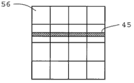
Fig. 4 A is the SIM image 51 in the cross section that obtains.In SIM image 51, device pattern 42 has appearred.Control part 11 utilizes dividing line 43 that SIM image 51 is divided into a plurality of zones.
Fig. 4 B is the SIM image 52 that obtains by proceeding cutting process.Defective 44 appears among the regional 52k.In response to this, change has occured in the image that control part 11 identifies in the zone only having SIM image 52.Control part 11 is end process at this moment.In this mode.Can be in the object of observation of wanting (being in this case defective 44) end process when being exposed in the cross section.
Semiconductor devices has various shapes, and therefore, the shape of the device pattern that will expose in the cross section changes in processing procedure.Be identified as mistakenly the appearance of the object of observation for the variation that prevents device pattern, end process when control part 11 does not detect image change in a plurality of zones.
Fig. 5 A is the SIM image 55 in the cross section that obtains.In SIM image 55, device pattern 42 has appearred.Control part 11 utilizes dividing line 43 that SIM image 55 is divided into a plurality of zones.Fig. 5 B is the SIM image 56 that obtains by proceeding cutting process.The device pattern 45 that its shape is different from device pattern 42 has appearred.In SIM image 56, to compare with SIM image 55, change has occured in image in a plurality of zones.In this case, control part 11 does not have end process.Afterwards, identify and only have in the situation that the image in the zone of carrying out the SIM image that cutting process obtains by further continuation changes defective and control part 11 occurring, control part 11 is end process at this moment.
Utilize this structure, cross section processing and finder can in addition therein device pattern shape each observe the cross section processing of different samples such as semiconductor devices in image and the situation of observing under also can be from observing image monitoring processing end point.
Next, with cross section processing and the finder described according to another embodiment of the present invention.
Except the processing of above-mentioned cross section and finder, cross section processing and finder in this embodiment also comprise EB lens barrel 1, and it is used for utilizing electron beam 8 irradiation samples 7, as shown in Figure 6.
Cross section processing and finder comprise that secondary electron detector 4 and backscattering electronic detectors 5 are as charged particle detector.Secondary electron detector 4 can detect by the irradiation of electron beam 8 or ion beam 9 secondary electron that generates from sample 7.Backscattering electronic detectors 5 are arranged on EB lens barrel 1 inside.Backscattering electronic detectors 5 can detect since electron beam 8 to the irradiation of sample 7 and by the backscattering electronics of sample 7 reflections.
Cross section processing and finder further comprise EB control part 12, FIB control part 13, image forming part 14 and display part 17.EB control part 12 sends to EB lens barrel 1 with project signal and comes radiating electron bundle 8 with control EB lens barrel 1.FIB control part 13 sends to FIB lens barrel 2 with project signal and comes radiation ion beam 9 with control FIB lens barrel 2.The signal formation backscattering electronic image of the backscattering electronics that image forming part 14 detects based on the signal that is used for scanning beam 8 that sends from EB control part 12 with by backscattering electronic detectors 5.Display part 17 can show the backscattering electronic image.The data of the signal formation SEM image of the secondary electron that image forming part 14 detects based on the signal that is used for scanning beam 8 that sends from EB control part 12 with by secondary electron detector 4.Display part 17 can show the SEM image.In addition, the data of the signal formation SIM image of the secondary electron that detects based on the signal that is used for ion beam 9 that sends from FIB control part 13 with by secondary electron detector 4 of image forming part 14.Display part 17 can show the SIM image.
According to this embodiment, can be in the situation that the sample stage 6 that do not tilt be utilized the cross section that is formed by ion beam 9 in the electron beam 8 irradiation cutting process, and can obtain the SEM image as the observation image.Therefore, compare with finder with the cross section processing that does not comprise EB lens barrel 1, can within the shorter time, carry out cross section processing and observation.
Claims (6)
1. a cross section processes and finder, and the processing of described cross section and finder comprise:
Sample stage, described sample stage is constructed to place sample thereon;
The focused ion beam lens barrel, described focused ion beam lens barrel is constructed to utilize the described sample of focused ion beam irradiation;
Charged particle detector, described charged particle detector are constructed to detect owing to the irradiation of described focused ion beam from the charged particle of described sample emission; And
Control part, described control part are constructed to repeatedly carry out processing and observe and process, and described processing and observation are processed and comprised:
Utilize described focused ion beam to cut the cutting process of described sample; And
Utilization is obtained the processing of obtaining of observing image from the described charged particle of the cross section emission of the described sample that forms by described cutting process,
Wherein, described control part is constructed to, and described observation image is divided into a plurality of zones, and
Wherein, described control part is constructed to, when first of a cross section of the described sample that is utilizing a processing and observe to process to obtain observe in the zone in a plurality of zones of image image with utilize another processing and observe second of another cross section of processing the described sample that obtains observe in a plurality of zones of image with a described regional corresponding zone in image between when variation having occurred, end process.
2. cross section according to claim 1 processes and finder,
Wherein, described control part is constructed to, when described first observe image and described the second observation image in two or more zones of image corresponding to the image in the zone of the observation image in described two or more zones between when variation having occurred, end process not.
3. cross section according to claim 1 processes and finder,
Wherein, described control part is constructed to described sample stage to utilize described focused ion beam to carry out described cutting process and describedly to obtain processing.
4. cross section according to claim 2 processes and finder,
Wherein, described control part is constructed to described sample stage to utilize described focused ion beam to carry out described cutting process and describedly to obtain processing.
5. cross section according to claim 1 processes and finder, and the processing of described cross section and finder further comprise:
The electron beam lens barrel, described electron beam lens barrel is used for utilizing the described cross section of electron beam irradiation,
Wherein, described observation image comprises the observation image that utilizes backscattering electronics that the irradiation owing to described electron beam generates and the side in the secondary electron to obtain.
6. cross section according to claim 2 processes and finder, and the processing of described cross section and finder further comprise:
The electron beam lens barrel, described electron beam lens barrel is constructed to utilize the described cross section of electron beam irradiation,
Wherein, described observation image comprises the observation image that utilizes backscattering electronics that the irradiation owing to described electron beam generates and the side in the secondary electron to obtain.
Applications Claiming Priority (2)
| Application Number | Priority Date | Filing Date | Title |
|---|---|---|---|
| JP2012068022A JP5990016B2 (en) | 2012-03-23 | 2012-03-23 | Cross-section processing observation device |
| JP2012-068022 | 2012-03-23 |
Publications (1)
| Publication Number | Publication Date |
|---|---|
| CN103323475A true CN103323475A (en) | 2013-09-25 |
Family
ID=49112347
Family Applications (1)
| Application Number | Title | Priority Date | Filing Date |
|---|---|---|---|
| CN201310093481.0A Pending CN103323475A (en) | 2012-03-23 | 2013-03-22 | Cross-section processing and observation apparatus |
Country Status (4)
| Country | Link |
|---|---|
| US (1) | US8637819B2 (en) |
| JP (1) | JP5990016B2 (en) |
| CN (1) | CN103323475A (en) |
| DE (1) | DE102013102666A1 (en) |
Cited By (2)
| Publication number | Priority date | Publication date | Assignee | Title |
|---|---|---|---|---|
| CN107976457A (en) * | 2017-11-18 | 2018-05-01 | 武汉钢铁有限公司 | Galvanized sheet overlay coating electron backscatter diffraction sample preparation methods |
| CN110243318A (en) * | 2018-03-07 | 2019-09-17 | 日本株式会社日立高新技术科学 | Section processing observation devices and methods therefor, program and process for measuring shape |
Families Citing this family (5)
| Publication number | Priority date | Publication date | Assignee | Title |
|---|---|---|---|---|
| JP6085150B2 (en) * | 2012-03-16 | 2017-02-22 | 株式会社日立ハイテクサイエンス | Sample preparation apparatus and sample preparation method |
| JP6529264B2 (en) * | 2014-01-22 | 2019-06-12 | 株式会社日立ハイテクサイエンス | Charged particle beam apparatus and sample observation method |
| JP6207081B2 (en) * | 2014-03-24 | 2017-10-04 | 株式会社日立ハイテクサイエンス | Focused ion beam device |
| JP6867015B2 (en) | 2017-03-27 | 2021-04-28 | 株式会社日立ハイテクサイエンス | Automatic processing equipment |
| KR102476186B1 (en) * | 2018-12-06 | 2022-12-12 | 주식회사 히타치하이테크 | charged particle beam device |
Family Cites Families (8)
| Publication number | Priority date | Publication date | Assignee | Title |
|---|---|---|---|---|
| JPS63119148A (en) * | 1986-11-07 | 1988-05-23 | Hitachi Ltd | Sample image display and record method and device |
| JP3246704B2 (en) * | 1995-02-27 | 2002-01-15 | シャープ株式会社 | Wiring board inspection equipment |
| JP3648384B2 (en) * | 1998-07-03 | 2005-05-18 | 株式会社日立製作所 | Focused ion beam processing method and processing apparatus |
| US6538249B1 (en) * | 1999-07-09 | 2003-03-25 | Hitachi, Ltd. | Image-formation apparatus using charged particle beams under various focus conditions |
| JP5105357B2 (en) * | 2007-11-01 | 2012-12-26 | エスアイアイ・ナノテクノロジー株式会社 | Defect recognition method, defect observation method, and charged particle beam apparatus |
| JP4965481B2 (en) * | 2008-02-15 | 2012-07-04 | エスアイアイ・ナノテクノロジー株式会社 | Composite charged particle beam apparatus, sample processing method using the same, and sample preparation method for transmission electron microscope |
| JP5352335B2 (en) * | 2009-04-28 | 2013-11-27 | 株式会社日立ハイテクノロジーズ | Compound charged particle beam system |
| JP2011054497A (en) * | 2009-09-03 | 2011-03-17 | Sii Nanotechnology Inc | Method and apparatus for cross-section processing and observation |
-
2012
- 2012-03-23 JP JP2012068022A patent/JP5990016B2/en active Active
-
2013
- 2013-03-15 DE DE102013102666A patent/DE102013102666A1/en not_active Withdrawn
- 2013-03-15 US US13/842,404 patent/US8637819B2/en active Active
- 2013-03-22 CN CN201310093481.0A patent/CN103323475A/en active Pending
Cited By (3)
| Publication number | Priority date | Publication date | Assignee | Title |
|---|---|---|---|---|
| CN107976457A (en) * | 2017-11-18 | 2018-05-01 | 武汉钢铁有限公司 | Galvanized sheet overlay coating electron backscatter diffraction sample preparation methods |
| CN107976457B (en) * | 2017-11-18 | 2020-08-07 | 武汉钢铁有限公司 | Preparation method of galvanized sheet surface coating electron back scattering diffraction sample |
| CN110243318A (en) * | 2018-03-07 | 2019-09-17 | 日本株式会社日立高新技术科学 | Section processing observation devices and methods therefor, program and process for measuring shape |
Also Published As
| Publication number | Publication date |
|---|---|
| US8637819B2 (en) | 2014-01-28 |
| JP5990016B2 (en) | 2016-09-07 |
| JP2013200987A (en) | 2013-10-03 |
| US20130248710A1 (en) | 2013-09-26 |
| DE102013102666A1 (en) | 2013-09-26 |
Similar Documents
| Publication | Publication Date | Title |
|---|---|---|
| CN103323475A (en) | Cross-section processing and observation apparatus | |
| JP3990981B2 (en) | Method and apparatus for inspecting a substrate | |
| EP2525386B1 (en) | Charged-particle microscopy with occlusion detection | |
| JP6002489B2 (en) | Charged particle beam apparatus and sample preparation method | |
| US10242842B2 (en) | Method for cross-section processing and observation and apparatus therefor | |
| US9966226B2 (en) | Cross-section processing and observation method and cross-section processing and observation apparatus | |
| CN103424419B (en) | Flying-spot microscope with adaptive scanning | |
| KR101987726B1 (en) | Electron-beam pattern inspection system | |
| US9983152B1 (en) | Material characterization using ion channeling imaging | |
| EP2924709A1 (en) | Imaging a sample with multiple beams and multiple detectors | |
| US10816333B2 (en) | Pattern measurement method and pattern measurement device | |
| US8853629B2 (en) | Cross-section processing and observation method and cross-section processing and observation apparatus | |
| KR20140010136A (en) | Apparatus and methods for real-time three-dimensional sem imaging and viewing of semiconductor wafers | |
| US10890545B2 (en) | Apparatus for combined stem and EDS tomography | |
| US20130134308A1 (en) | Sample observation apparatus and method of marking | |
| US9287087B2 (en) | Sample observation method, sample preparation method, and charged particle beam apparatus | |
| US9214316B2 (en) | Composite charged particle beam apparatus | |
| CN110494733B (en) | Automatic processing device | |
| WO2020105102A1 (en) | Imaging data analysis device | |
| US9329034B2 (en) | Pattern determination device and computer program | |
| US9470642B2 (en) | Crystal analysis apparatus, composite charged particle beam device, and crystal analysis method | |
| US20240379327A1 (en) | Entropy based image processing for focused ion beam delayer – edge slices detection | |
| KR20230141642A (en) | Method and system for analyzing three-dimensional features | |
| JP2010257675A (en) | Electron beam device having line analysis function |
Legal Events
| Date | Code | Title | Description |
|---|---|---|---|
| C06 | Publication | ||
| PB01 | Publication | ||
| C02 | Deemed withdrawal of patent application after publication (patent law 2001) | ||
| WD01 | Invention patent application deemed withdrawn after publication |
Application publication date: 20130925 |