CN103311130B - A kind of amorphous metal oxide thin film transistor and its preparation method - Google Patents
A kind of amorphous metal oxide thin film transistor and its preparation method Download PDFInfo
- Publication number
- CN103311130B CN103311130B CN201310174836.9A CN201310174836A CN103311130B CN 103311130 B CN103311130 B CN 103311130B CN 201310174836 A CN201310174836 A CN 201310174836A CN 103311130 B CN103311130 B CN 103311130B
- Authority
- CN
- China
- Prior art keywords
- film
- layer
- metal oxide
- metal
- film transistor
- Prior art date
- Legal status (The legal status is an assumption and is not a legal conclusion. Google has not performed a legal analysis and makes no representation as to the accuracy of the status listed.)
- Active
Links
- 239000010409 thin film Substances 0.000 title claims abstract description 75
- 229910044991 metal oxide Inorganic materials 0.000 title claims abstract description 70
- 150000004706 metal oxides Chemical class 0.000 title claims abstract description 70
- 239000005300 metallic glass Substances 0.000 title claims abstract description 64
- 238000002360 preparation method Methods 0.000 title claims abstract description 30
- 239000010408 film Substances 0.000 claims abstract description 106
- 229910052751 metal Inorganic materials 0.000 claims abstract description 88
- 239000002184 metal Substances 0.000 claims abstract description 88
- 238000000034 method Methods 0.000 claims abstract description 55
- 239000000758 substrate Substances 0.000 claims abstract description 33
- 238000005530 etching Methods 0.000 claims abstract description 26
- 238000000151 deposition Methods 0.000 claims abstract description 18
- 238000002161 passivation Methods 0.000 claims abstract description 17
- 230000006641 stabilisation Effects 0.000 claims abstract description 12
- 238000011105 stabilization Methods 0.000 claims abstract description 12
- 239000010410 layer Substances 0.000 claims description 140
- 239000000243 solution Substances 0.000 claims description 25
- 239000007789 gas Substances 0.000 claims description 17
- VYPSYNLAJGMNEJ-UHFFFAOYSA-N Silicium dioxide Chemical compound O=[Si]=O VYPSYNLAJGMNEJ-UHFFFAOYSA-N 0.000 claims description 16
- 229910052782 aluminium Inorganic materials 0.000 claims description 16
- 239000010949 copper Substances 0.000 claims description 16
- 239000000463 material Substances 0.000 claims description 16
- XAGFODPZIPBFFR-UHFFFAOYSA-N aluminium Chemical group [Al] XAGFODPZIPBFFR-UHFFFAOYSA-N 0.000 claims description 15
- 239000002356 single layer Substances 0.000 claims description 14
- 229910052750 molybdenum Inorganic materials 0.000 claims description 13
- RYGMFSIKBFXOCR-UHFFFAOYSA-N Copper Chemical compound [Cu] RYGMFSIKBFXOCR-UHFFFAOYSA-N 0.000 claims description 12
- ZOKXTWBITQBERF-UHFFFAOYSA-N Molybdenum Chemical compound [Mo] ZOKXTWBITQBERF-UHFFFAOYSA-N 0.000 claims description 12
- RTAQQCXQSZGOHL-UHFFFAOYSA-N Titanium Chemical compound [Ti] RTAQQCXQSZGOHL-UHFFFAOYSA-N 0.000 claims description 12
- 229910052802 copper Inorganic materials 0.000 claims description 12
- 239000011733 molybdenum Substances 0.000 claims description 12
- 239000010936 titanium Substances 0.000 claims description 11
- 229910052719 titanium Inorganic materials 0.000 claims description 10
- GUVRBAGPIYLISA-UHFFFAOYSA-N tantalum atom Chemical compound [Ta] GUVRBAGPIYLISA-UHFFFAOYSA-N 0.000 claims description 9
- 239000004642 Polyimide Substances 0.000 claims description 8
- 230000004888 barrier function Effects 0.000 claims description 8
- 229920001721 polyimide Polymers 0.000 claims description 8
- 229910052715 tantalum Inorganic materials 0.000 claims description 8
- PNEYBMLMFCGWSK-UHFFFAOYSA-N Alumina Chemical compound [O-2].[O-2].[O-2].[Al+3].[Al+3] PNEYBMLMFCGWSK-UHFFFAOYSA-N 0.000 claims description 7
- 229910052581 Si3N4 Inorganic materials 0.000 claims description 7
- UZLYXNNZYFBAQO-UHFFFAOYSA-N oxygen(2-);ytterbium(3+) Chemical compound [O-2].[O-2].[O-2].[Yb+3].[Yb+3] UZLYXNNZYFBAQO-UHFFFAOYSA-N 0.000 claims description 7
- HQVNEWCFYHHQES-UHFFFAOYSA-N silicon nitride Chemical compound N12[Si]34N5[Si]62N3[Si]51N64 HQVNEWCFYHHQES-UHFFFAOYSA-N 0.000 claims description 7
- 239000000126 substance Substances 0.000 claims description 7
- 229910003454 ytterbium oxide Inorganic materials 0.000 claims description 7
- 229940075624 ytterbium oxide Drugs 0.000 claims description 7
- 229910000838 Al alloy Inorganic materials 0.000 claims description 6
- VYZAMTAEIAYCRO-UHFFFAOYSA-N Chromium Chemical compound [Cr] VYZAMTAEIAYCRO-UHFFFAOYSA-N 0.000 claims description 6
- PXHVJJICTQNCMI-UHFFFAOYSA-N Nickel Chemical compound [Ni] PXHVJJICTQNCMI-UHFFFAOYSA-N 0.000 claims description 6
- 239000000956 alloy Substances 0.000 claims description 6
- PCHJSUWPFVWCPO-UHFFFAOYSA-N gold Chemical compound [Au] PCHJSUWPFVWCPO-UHFFFAOYSA-N 0.000 claims description 6
- 239000010931 gold Substances 0.000 claims description 6
- 229910052760 oxygen Inorganic materials 0.000 claims description 6
- 239000000377 silicon dioxide Substances 0.000 claims description 6
- BQCADISMDOOEFD-UHFFFAOYSA-N Silver Chemical compound [Ag] BQCADISMDOOEFD-UHFFFAOYSA-N 0.000 claims description 5
- QVGXLLKOCUKJST-UHFFFAOYSA-N atomic oxygen Chemical compound [O] QVGXLLKOCUKJST-UHFFFAOYSA-N 0.000 claims description 5
- 239000011651 chromium Substances 0.000 claims description 5
- 229910052737 gold Inorganic materials 0.000 claims description 5
- 239000001301 oxygen Substances 0.000 claims description 5
- 238000009832 plasma treatment Methods 0.000 claims description 5
- 239000005020 polyethylene terephthalate Substances 0.000 claims description 5
- 229920000139 polyethylene terephthalate Polymers 0.000 claims description 5
- 239000004332 silver Substances 0.000 claims description 5
- WFKWXMTUELFFGS-UHFFFAOYSA-N tungsten Chemical compound [W] WFKWXMTUELFFGS-UHFFFAOYSA-N 0.000 claims description 5
- 239000010937 tungsten Substances 0.000 claims description 5
- XLYOFNOQVPJJNP-UHFFFAOYSA-N water Substances O XLYOFNOQVPJJNP-UHFFFAOYSA-N 0.000 claims description 5
- 229910052804 chromium Inorganic materials 0.000 claims description 4
- 230000007547 defect Effects 0.000 claims description 4
- 229910052733 gallium Inorganic materials 0.000 claims description 4
- 239000011521 glass Substances 0.000 claims description 4
- BPUBBGLMJRNUCC-UHFFFAOYSA-N oxygen(2-);tantalum(5+) Chemical compound [O-2].[O-2].[O-2].[O-2].[O-2].[Ta+5].[Ta+5] BPUBBGLMJRNUCC-UHFFFAOYSA-N 0.000 claims description 4
- 239000004065 semiconductor Substances 0.000 claims description 4
- 229910052709 silver Inorganic materials 0.000 claims description 4
- 229910052721 tungsten Inorganic materials 0.000 claims description 4
- GYHNNYVSQQEPJS-UHFFFAOYSA-N Gallium Chemical compound [Ga] GYHNNYVSQQEPJS-UHFFFAOYSA-N 0.000 claims description 3
- FYYHWMGAXLPEAU-UHFFFAOYSA-N Magnesium Chemical compound [Mg] FYYHWMGAXLPEAU-UHFFFAOYSA-N 0.000 claims description 3
- XUIMIQQOPSSXEZ-UHFFFAOYSA-N Silicon Chemical compound [Si] XUIMIQQOPSSXEZ-UHFFFAOYSA-N 0.000 claims description 3
- ATJFFYVFTNAWJD-UHFFFAOYSA-N Tin Chemical compound [Sn] ATJFFYVFTNAWJD-UHFFFAOYSA-N 0.000 claims description 3
- 229910052769 Ytterbium Inorganic materials 0.000 claims description 3
- QCWXUUIWCKQGHC-UHFFFAOYSA-N Zirconium Chemical compound [Zr] QCWXUUIWCKQGHC-UHFFFAOYSA-N 0.000 claims description 3
- 229910052735 hafnium Inorganic materials 0.000 claims description 3
- VBJZVLUMGGDVMO-UHFFFAOYSA-N hafnium atom Chemical compound [Hf] VBJZVLUMGGDVMO-UHFFFAOYSA-N 0.000 claims description 3
- 229910052747 lanthanoid Inorganic materials 0.000 claims description 3
- 150000002602 lanthanoids Chemical class 0.000 claims description 3
- 229910052749 magnesium Inorganic materials 0.000 claims description 3
- 239000011777 magnesium Substances 0.000 claims description 3
- 239000011259 mixed solution Substances 0.000 claims description 3
- 229910052759 nickel Inorganic materials 0.000 claims description 3
- 229920002120 photoresistant polymer Polymers 0.000 claims description 3
- 229920003229 poly(methyl methacrylate) Polymers 0.000 claims description 3
- 239000011112 polyethylene naphthalate Substances 0.000 claims description 3
- -1 polyethylene terephthalate Polymers 0.000 claims description 3
- 239000004926 polymethyl methacrylate Substances 0.000 claims description 3
- 229910052761 rare earth metal Inorganic materials 0.000 claims description 3
- 229910052710 silicon Inorganic materials 0.000 claims description 3
- 239000010703 silicon Substances 0.000 claims description 3
- PBCFLUZVCVVTBY-UHFFFAOYSA-N tantalum pentoxide Inorganic materials O=[Ta](=O)O[Ta](=O)=O PBCFLUZVCVVTBY-UHFFFAOYSA-N 0.000 claims description 3
- 229910052718 tin Inorganic materials 0.000 claims description 3
- 238000004506 ultrasonic cleaning Methods 0.000 claims description 3
- NAWDYIZEMPQZHO-UHFFFAOYSA-N ytterbium Chemical compound [Yb] NAWDYIZEMPQZHO-UHFFFAOYSA-N 0.000 claims description 3
- 229910052726 zirconium Inorganic materials 0.000 claims description 3
- 239000004411 aluminium Substances 0.000 claims 5
- 238000009413 insulation Methods 0.000 claims 5
- 238000001035 drying Methods 0.000 claims 2
- 239000012212 insulator Substances 0.000 claims 2
- VAJVDSVGBWFCLW-UHFFFAOYSA-N 3-Phenyl-1-propanol Chemical compound OCCCC1=CC=CC=C1 VAJVDSVGBWFCLW-UHFFFAOYSA-N 0.000 claims 1
- PMPVIKIVABFJJI-UHFFFAOYSA-N Cyclobutane Chemical compound C1CCC1 PMPVIKIVABFJJI-UHFFFAOYSA-N 0.000 claims 1
- DYUQAZSOFZSPHD-UHFFFAOYSA-N Phenylpropyl alcohol Natural products CCC(O)C1=CC=CC=C1 DYUQAZSOFZSPHD-UHFFFAOYSA-N 0.000 claims 1
- 239000011248 coating agent Substances 0.000 claims 1
- 238000000576 coating method Methods 0.000 claims 1
- 239000013078 crystal Substances 0.000 claims 1
- 239000003595 mist Substances 0.000 claims 1
- 239000000203 mixture Substances 0.000 claims 1
- 229920003207 poly(ethylene-2,6-naphthalate) Polymers 0.000 claims 1
- 230000002000 scavenging effect Effects 0.000 claims 1
- 229910002070 thin film alloy Inorganic materials 0.000 claims 1
- 239000011135 tin Substances 0.000 claims 1
- 238000000059 patterning Methods 0.000 abstract description 10
- 230000000087 stabilizing effect Effects 0.000 abstract description 6
- 238000004519 manufacturing process Methods 0.000 description 16
- 238000005240 physical vapour deposition Methods 0.000 description 12
- 238000000623 plasma-assisted chemical vapour deposition Methods 0.000 description 9
- 239000000470 constituent Substances 0.000 description 8
- 239000004973 liquid crystal related substance Substances 0.000 description 8
- 238000010586 diagram Methods 0.000 description 6
- TWNQGVIAIRXVLR-UHFFFAOYSA-N oxo(oxoalumanyloxy)alumane Chemical compound O=[Al]O[Al]=O TWNQGVIAIRXVLR-UHFFFAOYSA-N 0.000 description 5
- 229920001621 AMOLED Polymers 0.000 description 4
- 238000005516 engineering process Methods 0.000 description 4
- 239000011159 matrix material Substances 0.000 description 4
- 235000012239 silicon dioxide Nutrition 0.000 description 4
- 229910052814 silicon oxide Inorganic materials 0.000 description 4
- 238000001039 wet etching Methods 0.000 description 4
- 229910052681 coesite Inorganic materials 0.000 description 3
- 229910052906 cristobalite Inorganic materials 0.000 description 3
- 238000001312 dry etching Methods 0.000 description 3
- 229910052738 indium Inorganic materials 0.000 description 3
- 238000000206 photolithography Methods 0.000 description 3
- 210000002381 plasma Anatomy 0.000 description 3
- 229910052682 stishovite Inorganic materials 0.000 description 3
- 229910052905 tridymite Inorganic materials 0.000 description 3
- 229910052725 zinc Inorganic materials 0.000 description 3
- 229920002799 BoPET Polymers 0.000 description 2
- SZUOHNOXDOVVTI-UHFFFAOYSA-N C1=CCC1.C(=C)C1=CC=CC=C1 Chemical compound C1=CCC1.C(=C)C1=CC=CC=C1 SZUOHNOXDOVVTI-UHFFFAOYSA-N 0.000 description 2
- 229910004298 SiO 2 Inorganic materials 0.000 description 2
- 229910021417 amorphous silicon Inorganic materials 0.000 description 2
- 230000007812 deficiency Effects 0.000 description 2
- 239000011888 foil Substances 0.000 description 2
- 229910001316 Ag alloy Inorganic materials 0.000 description 1
- 229910001020 Au alloy Inorganic materials 0.000 description 1
- 229910000599 Cr alloy Inorganic materials 0.000 description 1
- 229910000881 Cu alloy Inorganic materials 0.000 description 1
- 229910001182 Mo alloy Inorganic materials 0.000 description 1
- 229910004205 SiNX Inorganic materials 0.000 description 1
- 229910001362 Ta alloys Inorganic materials 0.000 description 1
- 229910001069 Ti alloy Inorganic materials 0.000 description 1
- 229910001080 W alloy Inorganic materials 0.000 description 1
- 230000002378 acidificating effect Effects 0.000 description 1
- 239000002131 composite material Substances 0.000 description 1
- 230000007797 corrosion Effects 0.000 description 1
- 238000005260 corrosion Methods 0.000 description 1
- 229910052593 corundum Inorganic materials 0.000 description 1
- 230000002950 deficient Effects 0.000 description 1
- 238000002438 flame photometric detection Methods 0.000 description 1
- 150000002500 ions Chemical class 0.000 description 1
- 150000002739 metals Chemical class 0.000 description 1
- 238000001020 plasma etching Methods 0.000 description 1
- 229910021420 polycrystalline silicon Inorganic materials 0.000 description 1
- 229920005591 polysilicon Polymers 0.000 description 1
- 229910001936 tantalum oxide Inorganic materials 0.000 description 1
- 229910001845 yogo sapphire Inorganic materials 0.000 description 1
Images


Classifications
-
- H—ELECTRICITY
- H10—SEMICONDUCTOR DEVICES; ELECTRIC SOLID-STATE DEVICES NOT OTHERWISE PROVIDED FOR
- H10D—INORGANIC ELECTRIC SEMICONDUCTOR DEVICES
- H10D30/00—Field-effect transistors [FET]
- H10D30/60—Insulated-gate field-effect transistors [IGFET]
- H10D30/67—Thin-film transistors [TFT]
- H10D30/674—Thin-film transistors [TFT] characterised by the active materials
- H10D30/6755—Oxide semiconductors, e.g. zinc oxide, copper aluminium oxide or cadmium stannate
-
- H—ELECTRICITY
- H10—SEMICONDUCTOR DEVICES; ELECTRIC SOLID-STATE DEVICES NOT OTHERWISE PROVIDED FOR
- H10D—INORGANIC ELECTRIC SEMICONDUCTOR DEVICES
- H10D99/00—Subject matter not provided for in other groups of this subclass
Landscapes
- Thin Film Transistor (AREA)
Abstract
一种非晶金属氧化物薄膜晶体管及其制备方法,制备方法依次包括:a.在衬底上制备并图形化金属导电层作为栅极;b.在所述金属导电层上沉积第一绝缘薄膜作为栅极绝缘层;c.在所述栅极绝缘层上沉积非晶金属氧化物薄膜并图形化作为有源层;d.在所述有源层上沉积金属层然后图形化作为源、漏电极;e.对背沟道进行稳定化处理;f.在所述源、漏电极上沉积第二绝缘薄膜作为钝化层。本发明设置了背沟道稳定化处理步骤,能够降低源、漏电极刻蚀后在背沟道处的刻蚀残留和损伤,所制备的薄膜晶体管的稳定性高,且工艺简单、成本低廉。
An amorphous metal oxide thin film transistor and a preparation method thereof, the preparation method sequentially comprising: a. preparing and patterning a metal conductive layer on a substrate as a gate; b. depositing a first insulating film on the metal conductive layer As a gate insulating layer; c. Deposit an amorphous metal oxide film on the gate insulating layer and pattern it as an active layer; d. Deposit a metal layer on the active layer and then pattern it as a source and drain e. Stabilizing the back channel; f. Depositing a second insulating film on the source and drain electrodes as a passivation layer. The invention sets the back channel stabilization treatment step, which can reduce the etching residue and damage on the back channel after the source and drain electrodes are etched, and the prepared thin film transistor has high stability, simple process and low cost.
Description
技术领域 technical field
本发明涉及半导体技术领域,尤其涉及一种非晶金属氧化物薄膜晶体管及其制备方法。 The invention relates to the technical field of semiconductors, in particular to an amorphous metal oxide thin film transistor and a preparation method thereof.
背景技术 Background technique
近年来,新型平板显示(FPD)产业发展日新月异。消费者对于大尺寸、高分辨率平板显示的高需求量刺激着整个产业不断进行显示技术提升。而作为FPD产业核心技术的薄膜晶体管(TFT)背板技术,也在经历着深刻的变革。 In recent years, the new flat panel display (FPD) industry has developed rapidly. Consumers' high demand for large-size, high-resolution flat-panel displays has stimulated the entire industry to continuously improve display technologies. The thin-film transistor (TFT) backplane technology, which is the core technology of the FPD industry, is also undergoing profound changes.
传统的非晶硅(α-Si)TFT因为迁移率较低(一般小于0.5),难以实现高分辨率显示,正面临着被市场淘汰的命运;低温多晶硅(LTPS)TFT虽然迁移率高(50~150),但是一方面生产工艺复杂、设备投资昂贵,一方面在大尺寸显示中还存在着均匀性差、良品率低等问题,导致LTPS在大尺寸FPD领域的进一步发展举步维艰。相比之下,非晶金属氧化物薄膜晶体管(MOTFT)不仅具有较高的迁移率(在5~50 cm2/Vs左右),而且制作工艺简单,制造成本较低。因此MOTFT技术自诞生以来便备受业界瞩目。 The traditional amorphous silicon (α-Si) TFT is facing the fate of being eliminated from the market because of its low mobility (generally less than 0.5), and it is difficult to achieve high-resolution display; the low-temperature polysilicon (LTPS) TFT has a high mobility (50 ~150), but on the one hand, the production process is complicated and the equipment investment is expensive, on the other hand, there are still problems such as poor uniformity and low yield in large-size displays, which makes it difficult for LTPS to further develop in the field of large-size FPDs. In contrast, the amorphous metal oxide thin film transistor (MOTFT) not only has a high mobility (about 5-50 cm 2 /Vs), but also has a simple manufacturing process and a low manufacturing cost. Therefore, MOTFT technology has attracted the attention of the industry since its birth.
目前MOTFT主要使用的结构有背沟道刻蚀结构和刻蚀阻挡层结构。 背沟道刻蚀结构是在制作有源层之后,在有源层上沉积金属层,并且图形化作为源、漏电极。而刻蚀阻挡层结构是在有源层生成之后,先制作一层刻蚀阻挡层,再在之上沉积金属层并且图形化作为源漏电极。 At present, the main structures used in MOTFT are back channel etching structure and etching barrier layer structure. The back channel etching structure is to deposit a metal layer on the active layer after making the active layer, and pattern it as the source and drain electrodes. The etch stop layer structure is to make a layer of etch stop layer after the active layer is formed, and then deposit a metal layer on it and pattern it as the source and drain electrodes.
背沟道刻蚀结构制作工艺较为简单,并且与传统非晶硅制作工艺相同,设备投资和生产成本都较低廉。该结构被认为是,薄膜晶体管实现大规模量产和能够广泛使用的必然发展方向。 The manufacturing process of the back channel etching structure is relatively simple, and is the same as the traditional amorphous silicon manufacturing process, and the equipment investment and production costs are relatively low. This structure is considered to be an inevitable development direction for thin film transistors to achieve mass production and wide use.
但是当使用背沟道刻蚀结构时,要求在非晶金属氧化物薄膜上直接沉积金属薄膜,并且刻蚀形成源、漏电极。由于非晶金属氧化物薄膜极易受到后续工艺影响,所以使用背沟道刻蚀结构的薄膜晶体管能否具有良好的电学性能,是该结构能否实用的关键因素。 However, when using the back channel etching structure, it is required to directly deposit the metal film on the amorphous metal oxide film, and etch to form the source and drain electrodes. Since the amorphous metal oxide thin film is easily affected by the subsequent process, whether the thin film transistor using the back channel etching structure can have good electrical performance is a key factor for the practicality of the structure.
目前主要使用的刻蚀源、漏电极的方法包括:湿法刻蚀和干法刻蚀。对于湿法刻蚀方法,因为非晶金属氧化物极易受到酸性或碱性化学药液的腐蚀。所以现在还没有能够找到,能有效刻蚀源、漏电极金属层,同时又不损伤非晶金属氧化物的刻蚀液。有报道表明,将金属氧化物晶化,能够提高其抵抗刻蚀的能力,得到稳定的薄膜晶体管。但是多晶金属氧化物薄膜晶体管制作的工艺温度较高,器件均匀性可能受到晶界的影响而劣化。 The currently mainly used methods for etching source and drain electrodes include: wet etching and dry etching. For the wet etching method, because the amorphous metal oxide is extremely susceptible to corrosion by acidic or alkaline chemical solutions. Therefore, there is no etching solution that can effectively etch the metal layer of the source and drain electrodes without damaging the amorphous metal oxide. It has been reported that crystallizing metal oxides can improve their ability to resist etching and obtain stable thin film transistors. However, the manufacturing process temperature of the polycrystalline metal oxide thin film transistor is relatively high, and the uniformity of the device may be deteriorated due to the influence of the grain boundary.
对于干法刻蚀方法,通常干法刻蚀金属薄膜需要使用到高能或高腐蚀性的等离子体。这些等离子体极易在晶体管背沟道处造成损伤,可能导致意外掺杂,使得器件稳定性变差。所以,目前使用背沟道刻蚀结构的MOTFT实现产品化非常困难。 For the dry etching method, usually the dry etching of the metal thin film requires the use of high-energy or highly corrosive plasma. These plasmas can easily damage the back channel of the transistor, which can lead to unintentional doping and degrade device stability. Therefore, it is very difficult to commercialize the MOTFT using the back channel etching structure at present.
使用刻蚀阻挡层结构的MOTFT可以很大程度地避免上述问题, 因此它的稳定性比较好,目前该结构薄膜晶体管已商业化。但是因为其需要增加额外的光刻掩膜版制作刻蚀阻挡层,导致工艺复杂,制作成本高。 The MOTFT with an etching barrier structure can avoid the above problems to a large extent, so its stability is relatively good, and the thin film transistor with this structure has been commercialized at present. However, because it needs to add an additional photolithographic mask to make the etching barrier layer, the process is complicated and the manufacturing cost is high.
因此,针对现有技术不足,提供一种稳定性好、制备工艺简单、成本低廉的薄膜晶体管及其制备方法以克服现有技术不足甚为必要。 Therefore, aiming at the deficiencies of the prior art, it is necessary to provide a thin film transistor with good stability, simple manufacturing process and low cost and a manufacturing method thereof to overcome the deficiencies of the prior art.
发明内容 Contents of the invention
本发明的目的之一是提供了一种非晶金属氧化物薄膜晶体管的制备方法,该制备方法具有制备工艺简单、成本低廉且所制备的非晶金属氧化物薄膜晶体管稳定性高的特点。 One of the objects of the present invention is to provide a preparation method of an amorphous metal oxide thin film transistor, which has the characteristics of simple preparation process, low cost and high stability of the prepared amorphous metal oxide thin film transistor.
本发明的上述目的通过如下技术手段实现。 The above object of the present invention is achieved through the following technical means.
一种非晶金属氧化物薄膜晶体管的制备方法,依次包括如下步骤: A method for preparing an amorphous metal oxide thin film transistor, comprising the following steps in sequence:
a.在衬底上制备并图形化金属导电层作为栅极; a. preparing and patterning a metal conductive layer on the substrate as a gate;
b.在所述金属导电层上沉积第一绝缘薄膜作为栅极绝缘层; b. Depositing a first insulating film on the metal conductive layer as a gate insulating layer;
c.在所述栅极绝缘层上沉积非晶金属氧化物薄膜并图形化作为有源层; c. Depositing an amorphous metal oxide film on the gate insulating layer and patterning it as an active layer;
d.在所述有源层上沉积金属层然后图形化作为源、漏电极; d. Depositing a metal layer on the active layer and then patterning it as source and drain electrodes;
e.对背沟道进行稳定化处理; e. Stabilize the back channel;
f.在所述源、漏电极上沉积第二绝缘薄膜作为钝化层。 f. Depositing a second insulating film as a passivation layer on the source and drain electrodes.
上述步骤e对背沟道进行稳定化处理包括清除背沟道处的刻蚀残留和钝化背沟道处的缺陷态中的至少一项。 The stabilization treatment of the back channel in the above step e includes at least one of removing the etching residue in the back channel and passivating the defect states in the back channel.
优选的,上述湿法处理具体是使用H2O2溶液或者KOH溶液或者NaF溶液,或者使用以上溶液中任意两种以上的混合溶液对背沟道进行超声清洗; Preferably, the above-mentioned wet treatment specifically uses H 2 O 2 solution or KOH solution or NaF solution, or uses any two or more mixed solutions of the above solutions to ultrasonically clean the back channel;
所述H2O2浓度范围:1 wt%~30 wt%,KOH溶液浓度范围:0.1 wt%~5 wt%,NaF溶液浓度范围:0.1 wt%~10 wt%。 The H 2 O 2 concentration range: 1 wt% to 30 wt%, the KOH solution concentration range: 0.1 wt% to 5 wt%, and the NaF solution concentration range: 0.1 wt% to 10 wt%.
超声清洗时间设置为1至10分钟。 The ultrasonic cleaning time was set from 1 to 10 minutes.
另一优选的,上述步骤e干法处理具体是采用气体进行等离子体处理,所采用的气体为C3F8、Ar、SF6、CF4或CHF3单种气体,或者为C3F8、Ar、SF6、CF4、CHF3中的任意两种以上的混合气体,或者为C3F8、Ar、SF6、CF4、CHF3中的至少一种气体与O2、N2O中的任意一种组成的混合气体。 In another preferred embodiment, the dry treatment in step e above specifically uses gas for plasma treatment, and the gas used is a single gas of C 3 F 8 , Ar, SF 6 , CF 4 or CHF 3 , or C 3 F 8 , Ar, SF 6 , CF 4 , CHF 3 any two or more mixed gases, or at least one gas of C 3 F 8 , Ar, SF 6 , CF 4 , CHF 3 and O 2 , N 2 A mixed gas composed of any one of O.
等离子体处理的时间设置为10分钟以内。 The plasma treatment time is set within 10 minutes.
上述步骤a中衬底设置为具有缓冲层的玻璃衬底或者具有水氧阻隔层的柔性衬底; The substrate in the above step a is set as a glass substrate with a buffer layer or a flexible substrate with a water and oxygen barrier layer;
当所述衬底为柔性衬底时,柔性衬底具体设置为聚萘二甲酸乙二醇酯(PEN)、聚对苯二甲酸乙二酯(PET)、聚酰亚胺(PI)或者金属箔柔性衬底;所述步骤a中在衬底上制备并图形化金属导电层所使用的金属为铝、铜、钼、钛、银、金、钽、钨、铬单质或铝合金; When the substrate is a flexible substrate, the flexible substrate is specifically set to be polyethylene naphthalate (PEN), polyethylene terephthalate (PET), polyimide (PI) or metal Foil flexible substrate; the metal used for preparing and patterning the metal conductive layer on the substrate in the step a is aluminum, copper, molybdenum, titanium, silver, gold, tantalum, tungsten, chromium element or aluminum alloy;
所述金属导电层为单层铝薄膜、铜薄膜、钼薄膜、钛薄膜、银薄膜、金薄膜、钽薄膜、钨薄膜、铬薄膜或铝合金薄膜;或者是由以上单层金属薄膜构成的两层以上的薄膜; The metal conductive layer is a single-layer aluminum film, copper film, molybdenum film, titanium film, silver film, gold film, tantalum film, tungsten film, chromium film or aluminum alloy film; more than one layer of film;
所述金属导电层的厚度设置为100 nm至2000 nm; The thickness of the metal conductive layer is set to 100 nm to 2000 nm;
所述金属导电层作为薄膜晶体管栅极。 The metal conductive layer is used as the gate of the thin film transistor.
上述步骤b中的所述第一绝缘薄膜的厚度为50 nm至500 nm; The thickness of the first insulating film in the above step b is 50 nm to 500 nm;
所述第一绝缘薄膜为氧化硅、氮化硅、氧化铝、五氧化二钽或氧化镱绝缘薄膜的单层薄膜,或者是由以上材料的任意组合构成的两层以上的薄膜; The first insulating film is a single-layer film of silicon oxide, silicon nitride, aluminum oxide, tantalum pentoxide or ytterbium oxide insulating film, or a film of more than two layers composed of any combination of the above materials;
所述步骤c中的所述有源层厚度为20 nm至200 nm; The thickness of the active layer in the step c is 20 nm to 200 nm;
构成所述有源层的半导体材料是金属氧化物(In2O3)x(MO)y(ZnO)z,其中0≤x≤1,0≤y≤1,0≤z≤1,且x+y+z=1,M为镓、锡、硅、铝、镁、钽、铪、镱、镍、锆或镧系稀土元素中的一种或两种以上的任意组合; The semiconductor material constituting the active layer is metal oxide (In 2 O 3 ) x (MO) y (ZnO) z , where 0≤x≤1, 0≤y≤1, 0≤z≤1, and x +y+z=1, M is one or any combination of two or more of gallium, tin, silicon, aluminum, magnesium, tantalum, hafnium, ytterbium, nickel, zirconium or lanthanide rare earth elements;
所述步骤d中沉积所述金属层所使用的金属为铝、铜、钼、钛单质,或由以上金属单质作为主体的合金材料; The metal used for depositing the metal layer in the step d is aluminum, copper, molybdenum, titanium element, or an alloy material mainly composed of the above metal element;
所述金属层为单层铝薄膜、铜薄膜、钼薄膜、钛薄膜或由以上金属单质作为主体的合金材料膜,或者由以上单层金属薄膜构成的两层以上的薄膜; The metal layer is a single-layer aluminum film, copper film, molybdenum film, titanium film or an alloy material film mainly composed of the above metal simple substance, or a film consisting of more than two layers of the above single-layer metal film;
所述金属层的厚度为100 nm~2000 nm。 The metal layer has a thickness of 100 nm to 2000 nm.
上述钝化层的厚度为50 nm~2000 nm; The thickness of the passivation layer is 50 nm to 2000 nm;
所述钝化层为氧化硅、氮化硅、氧化铝、氧化镱、聚酰亚胺、光刻胶、苯丙环丁烯或聚甲基丙烯酸甲酯单层薄膜,或者是由以上材料的任意组合构成的两层以上的薄膜。 The passivation layer is silicon oxide, silicon nitride, aluminum oxide, ytterbium oxide, polyimide, photoresist, styrene cyclobutene or polymethyl methacrylate monolayer film, or is made of the above materials Any combination of two or more layers of film.
本发明的非晶金属氧化物薄膜晶体管的制备方法,依次包括如下步骤:a.在衬底上制备并图形化金属导电层作为栅极;b.在所述金属导电层上沉积第一绝缘薄膜作为栅极绝缘层;c.在所述栅极绝缘层上沉积非晶金属氧化物薄膜并图形化作为有源层;d.在所述有源层上沉积金属层然后图形化作为源、漏电极;e.对背沟道进行稳定化处理;f.在所述源、漏电极上沉积第二绝缘薄膜作为钝化层。本发明在背沟道刻蚀型非晶金属氧化物薄膜晶体管的制备过程中,引入了背沟道稳定化处理步骤,背沟道稳定化处理能够降低源、漏电极刻蚀后在背沟道处的刻蚀残留和损伤,故本发明的方法所制备的非晶金属氧化物薄膜晶体管的稳定性高,而且本发明的方法工艺简单、成本低廉。 The preparation method of the amorphous metal oxide thin film transistor of the present invention comprises the following steps in sequence: a. preparing and patterning a metal conductive layer on a substrate as a gate; b. depositing a first insulating film on the metal conductive layer As a gate insulating layer; c. Deposit an amorphous metal oxide film on the gate insulating layer and pattern it as an active layer; d. Deposit a metal layer on the active layer and then pattern it as a source and drain e. Stabilizing the back channel; f. Depositing a second insulating film on the source and drain electrodes as a passivation layer. In the preparation process of the back channel etching type amorphous metal oxide thin film transistor, the present invention introduces a back channel stabilizing treatment step, and the back channel stabilizing treatment can reduce the source and drain electrodes in the back channel after etching. Therefore, the amorphous metal oxide thin film transistor prepared by the method of the present invention has high stability, and the method of the present invention has simple process and low cost.
本发明提供的非晶金属氧化物薄膜晶体管,采用上述的方法制备而成。所制备的非晶金属氧化物薄膜晶体管的稳定性大大提高,满足了薄膜晶体管产品化的要求,而且制备工艺简单、成本低廉。 The amorphous metal oxide thin film transistor provided by the present invention is prepared by the above-mentioned method. The stability of the prepared amorphous metal oxide thin film transistor is greatly improved, which meets the requirement of commercialization of the thin film transistor, and the preparation process is simple and the cost is low. the
附图说明 Description of drawings
利用附图对本发明作进一步的说明,但附图中的内容不构成对本发明的任何限制。 The present invention will be further described by using the accompanying drawings, but the content in the accompanying drawings does not constitute any limitation to the present invention.
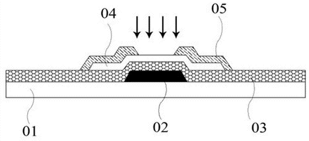
图1是本发明实施例的沉积并图形化金属导电层作为栅极的示意图 Figure 1 is a schematic diagram of depositing and patterning a metal conductive layer as a gate according to an embodiment of the present invention
图2是本发明实施例的在金属导电层上沉积第一绝缘膜作为栅极绝缘层的示意图; 2 is a schematic diagram of depositing a first insulating film on a metal conductive layer as a gate insulating layer according to an embodiment of the present invention;
图3是本发明实施例的沉积有源层的示意图; Fig. 3 is a schematic diagram of depositing an active layer according to an embodiment of the present invention;
图4是本发明实施例的图形化源漏电极的示意图; 4 is a schematic diagram of a patterned source-drain electrode according to an embodiment of the present invention;
图5 是本发明实施例的背沟道稳定化处理的示意图; Fig. 5 is the schematic diagram of the back channel stabilization treatment of the embodiment of the present invention;
图6是本发明实施例的制作钝化层的示意图。 FIG. 6 is a schematic diagram of forming a passivation layer according to an embodiment of the present invention.
在图1至图6中,包括: In Figures 1 to 6, including:
衬底01、
栅极02、
第一绝缘薄膜03、
The first insulating
有源层04、
图形化成源、漏电极的金属层05、
The
钝化层06。
具体实施方式 Detailed ways
结合以下实施例对本发明作进一步描述。 The present invention is further described in conjunction with the following examples.
实施例1。Example 1.
一种非晶金属氧化物薄膜晶体管的制备方法,依次包括如下步骤。 A method for preparing an amorphous metal oxide thin film transistor comprises the following steps in sequence.
a.在衬底上制备并图形化金属导电层作为栅极。 a. Preparing and patterning a metal conductive layer on the substrate as a gate.
具体的,步骤a中衬底设置为具有缓冲层的玻璃衬底或者具有水氧阻隔层的柔性衬底。 Specifically, the substrate in step a is set as a glass substrate with a buffer layer or a flexible substrate with a water and oxygen barrier layer.
当所述衬底为柔性衬底时,柔性衬底具体设置为聚萘二甲酸乙二醇酯(PEN)、聚对苯二甲酸乙二酯(PET)、聚酰亚胺(PI)或者金属箔柔性衬底。 When the substrate is a flexible substrate, the flexible substrate is specifically set to be polyethylene naphthalate (PEN), polyethylene terephthalate (PET), polyimide (PI) or metal foil flexible substrate.
步骤a中在衬底上制备并图形化金属导电层所使用的金属为铝、铜、钼、钛、银、金、钽、钨、铬单质或铝合金。 The metal used for preparing and patterning the metal conductive layer on the substrate in step a is aluminum, copper, molybdenum, titanium, silver, gold, tantalum, tungsten, chromium or aluminum alloy.
金属导电层为单层铝薄膜、铜薄膜、钼薄膜、钛薄膜、银薄膜、金薄膜、钽薄膜、钨薄膜、铬薄膜或铝合金薄膜;或者是由以上单层金属薄膜构成的两层以上的薄膜。 The metal conductive layer is a single-layer aluminum film, copper film, molybdenum film, titanium film, silver film, gold film, tantalum film, tungsten film, chromium film or aluminum alloy film; or two or more layers of the above single-layer metal film film.
金属导电层的厚度设置为100 nm至2000 nm,金属导电层作为非晶金属氧化物薄膜晶体管栅极。 The thickness of the metal conductive layer is set to 100 nm to 2000 nm, and the metal conductive layer is used as the gate of the amorphous metal oxide thin film transistor.
完成栅极的制作后,就进入步骤b。 After the fabrication of the grid is completed, step b is entered.
b.在所述金属导电层上沉积第一绝缘薄膜作为栅极绝缘层。 b. Depositing a first insulating film as a gate insulating layer on the metal conductive layer.
第一绝缘薄膜的厚度为50 nm至500 nm,第一绝缘薄膜为氧化硅、氮化硅、氧化铝、五氧化二钽或氧化镱绝缘薄膜的单层薄膜,或者是由以上材料的任意组合构成的两层以上的薄膜。 The thickness of the first insulating film is 50 nm to 500 nm, and the first insulating film is a single-layer film of silicon oxide, silicon nitride, aluminum oxide, tantalum pentoxide or ytterbium oxide insulating film, or any combination of the above materials A film composed of more than two layers.
接着,进入步骤c。 Next, go to step c.
c.在所述栅极绝缘层上沉积非晶金属氧化物薄膜并图形化作为有源层。 c. Depositing an amorphous metal oxide film on the gate insulating layer and patterning it as an active layer.
有源层厚度为20 nm至200 nm,构成所述有源层的半导体材料是金属氧化物(In2O3)x(MO)y(ZnO)z,其中0≤x≤1,0≤y≤1,0≤z≤1,且x+y+z=1,M为镓、锡、硅、铝、镁、钽、铪、镱、镍、锆或镧系稀土元素中的一种或两种以上的任意组合。 The thickness of the active layer is 20 nm to 200 nm, and the semiconductor material constituting the active layer is metal oxide (In 2 O 3 ) x (MO) y (ZnO) z , where 0≤x≤1, 0≤y ≤1, 0≤z≤1, and x+y+z=1, M is one or both of gallium, tin, silicon, aluminum, magnesium, tantalum, hafnium, ytterbium, nickel, zirconium or lanthanide rare earth elements Any combination of the above.
d.在有源层上沉积金属层然后图形化作为源、漏电极。 d. Deposit a metal layer on the active layer and then pattern it as source and drain electrodes.
所述步骤d中沉积所述金属层所使用的金属为铝、铜、钼、钛单质,或由以上金属单质作为主体的合金材料。 The metal used for depositing the metal layer in the step d is aluminum, copper, molybdenum, titanium, or an alloy material mainly composed of the above metals.
导电薄膜层为单层铝薄膜、铜薄膜、钼薄膜、钛薄膜或由以上金属单质作为主体的合金材料膜,或者由以上单层金属薄膜构成的两层以上的薄膜。 The conductive thin film layer is a single-layer aluminum thin film, copper thin film, molybdenum thin film, titanium thin film, or an alloy material film mainly composed of the above metal simple substance, or a film composed of more than two layers of the above single-layer metal thin film.
金属层的厚度为100 nm~2000 nm。 The thickness of the metal layer is 100 nm to 2000 nm.
e.对背沟道进行稳定化处理。 e. Stabilize the back channel.
对背沟道进行稳定化处理包括清除背沟道处的刻蚀残留和钝化背沟道处的缺陷态中的至少一项。可以是进行清除背沟道处的刻蚀残留;也可以是钝化背沟道处的缺陷态;也可以为既进行清除背沟道处的刻蚀残留,又进行钝化背沟道处的缺陷态。 Stabilizing the back channel includes at least one of removing etching residues in the back channel and passivating defect states in the back channel. It can be to remove the etching residue at the back channel; it can also be to passivate the defect state at the back channel; it can also be to remove the etching residue at the back channel and passivate the defective state.
对背沟道进行稳定化处理,具体可以采用湿法处理和干法处理。 The back channel is stabilized, and specifically, wet treatment and dry treatment can be used.
采用湿法处理对背沟道进行稳定化处理,具体操作方法为,使用H2O2溶液 或者KOH溶液或者NaF溶液对背沟道进行超声清洗不超于10分钟。 The back channel is stabilized by wet treatment, and the specific operation method is to use H 2 O 2 solution or KOH solution or NaF solution to ultrasonically clean the back channel for no more than 10 minutes.
其中,H2O2浓度范围:1 wt%~30 wt%,KOH溶液浓度范围:0.1 wt%~5 wt%,NaF溶液浓度范围:0.1 wt%~10 wt%。 Among them, the concentration range of H 2 O 2 is 1 wt%~30 wt%, the concentration range of KOH solution is 0.1 wt%~5 wt%, and the concentration range of NaF solution is 0.1 wt%~10 wt%.
也可以采用干法处理对背沟道进行稳定化处理,具体是采用气体进行等离子体处理1至10分钟,所采用的气体为C3F8、Ar、SF6、CF4或CHF3单种气体,或者为C3F8、Ar、SF6、CF4、CHF3中的任意两种以上的混合气体,或者为C3F8、Ar、SF6、CF4、CHF3中的至少一种气体与O2、N2O中的任意一种组成的混合气体。 The back channel can also be stabilized by dry treatment, specifically, the gas is used for plasma treatment for 1 to 10 minutes, and the gas used is C 3 F 8 , Ar, SF 6 , CF 4 or CHF 3 Gas, or a mixed gas of any two or more of C 3 F 8 , Ar, SF 6 , CF 4 , CHF 3 , or at least one of C 3 F 8 , Ar, SF 6 , CF 4 , CHF 3 A mixed gas composed of one gas and any one of O 2 and N 2 O.
通过背沟道稳定化处理,能够降低源、漏电极刻蚀后在背沟道处的刻蚀残留和损伤,提高所制备的非晶金属氧化物薄膜晶体管的稳定性。 The back channel stabilization treatment can reduce the etching residue and damage on the back channel after the source and drain electrodes are etched, and improve the stability of the prepared amorphous metal oxide thin film transistor.
f.在所述源、漏电极上沉积第二绝缘薄膜作为钝化层。 f. Depositing a second insulating film as a passivation layer on the source and drain electrodes.
钝化层的厚度为50 nm~2000 nm,钝化层为氧化硅、氮化硅、氧化铝、氧化镱、聚酰亚胺、光刻胶、苯丙环丁烯或聚甲基丙烯酸甲酯单层薄膜,或者是由以上材料的任意组合构成的两层以上的薄膜。 The thickness of the passivation layer is 50 nm~2000 nm, and the passivation layer is silicon oxide, silicon nitride, aluminum oxide, ytterbium oxide, polyimide, photoresist, styrene-cyclobutene or polymethyl methacrylate A single-layer film, or a film with more than two layers composed of any combination of the above materials.
本发明在背沟道刻蚀型非晶金属氧化物薄膜晶体管的制备过程中,打破传统常规引入了背沟道稳定化处理步骤,并通过大量实践寻求进行背沟道稳定化处理的优选方案,背沟道稳定化处理能够降低源、漏电极刻蚀后在背沟道处的刻蚀残留和损伤,故本发明的方法所制备的非晶金属氧化物薄膜晶体管的稳定性高。同时,本发明的方法在进行背沟道稳定化处理过程中,不需要特殊的设备,故,本发明的方法工艺简单、成本低廉。所制备的非晶金属氧化物薄膜晶体管也具有稳定性高,制备工艺简单、成本低廉的特点。 In the preparation process of the back channel etching type amorphous metal oxide thin film transistor, the present invention breaks the traditional routine and introduces a back channel stabilization treatment step, and seeks an optimal solution for the back channel stabilization treatment through a lot of practice, The back channel stabilization treatment can reduce the etching residue and damage on the back channel after the source and drain electrodes are etched, so the amorphous metal oxide thin film transistor prepared by the method of the present invention has high stability. At the same time, the method of the present invention does not require special equipment during the process of stabilizing the back channel, so the method of the present invention is simple in process and low in cost. The prepared amorphous metal oxide thin film transistor also has the characteristics of high stability, simple preparation process and low cost. the
实施例2。Example 2.
一种非晶金属氧化物薄膜晶体管的制备方法,包括如下工序。 A method for preparing an amorphous metal oxide thin film transistor includes the following steps.
如图1所示,在带有200 nm厚的SiO2缓冲层的无碱玻璃衬底01上,使用PVD(Physical Vapor Deposition)法依次沉积Mo/Al/Mo三层金属薄膜作为金属导电层,厚度分别为25 nm/100 nm/25 nm。使用光刻工艺将金属导电层图形化作为栅极02。
As shown in Figure 1, on an alkali-
需要说明的是,金属导电层的厚度范围在100 nm至2000 nm范围内, 其具体尺寸可以根据实际需要灵活设置,不限于本实施例的尺寸。金属导电层的构成材料也不限于本实施例的情况。 It should be noted that the thickness of the metal conductive layer ranges from 100 nm to 2000 nm, and its specific size can be flexibly set according to actual needs, and is not limited to the size of this embodiment. The constituent material of the metal conductive layer is also not limited to the case of this embodiment.
接着,如图2所示,在已图形化的金属导电层上,使用PECVD法(Plasma Enhanced Chemical Vapor Deposition)沉积第一绝缘膜03,第一绝缘膜03由300 nm的SiNx和30 nm的SiO2叠层而成作为栅极绝缘层。需要说明的是,第一绝缘膜的厚度范围在50 nm至500 nm范围内, 其具体尺寸可以根据实际需要灵活设置,不限于本实施例的尺寸,第一绝缘膜的构成材料也不限于本实施例的情况。
Next, as shown in FIG. 2, on the patterned metal conductive layer, use PECVD (Plasma Enhanced Chemical Vapor Deposition) to deposit a first insulating
接着,使用PVD法沉积50 nm非晶金属氧化物IZO薄膜(In、Zn原子比为1:1)作为有源层04,如图3所示。
Next, a 50 nm amorphous metal oxide IZO film (the atomic ratio of In and Zn is 1:1) was deposited by PVD method as the
需要说明的是,有源层的厚度范围在20 nm至200 nm范围内,其具体尺寸可以根据实际需要灵活设置,不限于本实施例的尺寸。有源层的构成材料也不限于本实施例的情况。 It should be noted that the active layer has a thickness ranging from 20 nm to 200 nm, and its specific size can be flexibly set according to actual needs, and is not limited to the size of this embodiment. The constituent material of the active layer is also not limited to the case of this embodiment.
如图4所示,使用PVD法制备Mo/Al/Mo叠层金属层,厚度分别为25 nm/100nm/25nm。使用30%的H2O2和1%的KOH作为湿法刻蚀药液,分别刻蚀叠层金属层中的Mo和Al,使用该方法将Mo/Al/Mo图形化形成源、漏电极的金属层05。
As shown in Figure 4, the Mo/Al/Mo laminated metal layer was prepared by PVD method, with thicknesses of 25 nm/100 nm/25 nm, respectively. Use 30% H 2 O 2 and 1% KOH as the wet etching solution to etch Mo and Al in the laminated metal layer respectively, and use this method to pattern Mo/Al/Mo to form source and drain
然后,如图5所示,使用Ar与O2混合离子体对非晶金属氧化物薄膜晶体管背沟道进行稳定化处理。处理条件为:Ar/O2为100:20,在功率300W的条件下进行5分钟处理。 Then, as shown in FIG. 5 , the back channel of the amorphous metal oxide thin film transistor is stabilized by using mixed ions of Ar and O 2 . The treatment conditions are: Ar/O 2 is 100:20, and the treatment is performed for 5 minutes under the condition of a power of 300W.
最后,如图6所示, 使用PECVD沉积厚度为300 nm的SiO2作为钝化层06,完成非晶金属氧化物薄膜晶体管的制作。
Finally, as shown in FIG. 6 , use PECVD to deposit SiO 2 with a thickness of 300 nm as the
本发明在背沟道刻蚀型非晶金属氧化物薄膜晶体管的制备过程中,引入了背沟道稳定化处理步骤,背沟道稳定化处理能够降低源、漏电极刻蚀后再背沟道处的刻蚀残留和损伤,故本发明的方法所制备的非晶金属氧化物薄膜晶体管的稳定性高,而且本发明的方法工艺简单、成本低廉。 The present invention introduces a back channel stabilization treatment step in the preparation process of the back channel etching type amorphous metal oxide thin film transistor. Therefore, the amorphous metal oxide thin film transistor prepared by the method of the present invention has high stability, and the method of the present invention has simple process and low cost. the
该工艺制作的非晶金属氧化物薄膜晶体管,可以用于液晶显示器LCD (Liquid Crystal Display)以及主动矩阵有机发光二极体面板AMOLED (Active Matrix/Organic Light Emitting Diode)领域。 The amorphous metal oxide thin film transistor produced by this process can be used in the field of liquid crystal display LCD (Liquid Crystal Display) and active matrix organic light emitting diode panel AMOLED (Active Matrix/Organic Light Emitting Diode).
需要说明的是,本实施例中涉及的尺寸、配比比例并不限制本发明非晶金属氧化物薄膜晶体管的制备工艺,在实际制备过程中,使用者可以根据具体需要灵活调整。 It should be noted that the dimensions and proportions involved in this embodiment do not limit the preparation process of the amorphous metal oxide thin film transistor of the present invention, and users can flexibly adjust according to specific needs during the actual preparation process. the
实施例3。Example 3.
一种非晶金属氧化物薄膜晶体管的制备方法,包括如下工序。 A method for preparing an amorphous metal oxide thin film transistor includes the following steps.
如图1所示,在带有50 nm的Al2O3水氧阻隔层的柔性PET薄膜的衬底01上,使用PVD(Physical Vapor Deposition)法沉积厚度为500 nm的Cu膜作为金属导电层。使用光刻工艺将金属导电层图形化作为栅极02。需要说明的是,金属导电层的厚度范围在100 nm至2000 nm范围内, 其具体尺寸可以根据实际需要灵活设置,不限于本实施例的尺寸。金属导电层的构成材料也不限于本实施例的情况。
As shown in Figure 1, on the flexible
接着,如图2所示,在已图形化的金属导电层上,使用PECVD法(Plasma Enhanced Chemical Vapor Deposition)沉积第一绝缘膜03,第一绝缘膜03由200 nm的氧化铝和100 nm的氧化镱叠层而成作为栅极绝缘层。需要说明的是, 第一绝缘膜的厚度范围在50 nm至500 nm范围内, 其具体尺寸可以根据实际需要灵活设置, 不限于本实施例的尺寸,第一绝缘膜的构成材料也不限于本实施例的情况。
Next, as shown in Figure 2, on the patterned metal conductive layer, use the PECVD method (Plasma Enhanced Chemical Vapor Deposition) to deposit the first insulating
接着,使用PVD法沉积50 nm非晶金属氧化物IGZO薄膜(In、Ga、Zn原子比为1:1:1)作为有源层04,如图3所示。
Next, a 50 nm amorphous metal oxide IGZO film (the atomic ratio of In, Ga, and Zn is 1:1:1) was deposited by PVD method as the
需要说明的是,有源层的厚度范围在20 nm至200 nm范围内,其具体尺寸可以根据实际需要灵活设置,不限于本实施例的尺寸。有源层的构成材料也不限于本实施例的情况。 It should be noted that the active layer has a thickness ranging from 20 nm to 200 nm, and its specific size can be flexibly set according to actual needs, and is not limited to the size of this embodiment. The constituent material of the active layer is also not limited to the case of this embodiment.
如图4所示,使用PVD法制备Mo/Cu叠层金属层,厚度分别为25 nm/2000nm。使用30%的H2O2和30%的FeCl3作为湿法刻蚀药液,分别刻蚀叠层金属中的Mo和Cu。使用该方法具有将Mo/Cu图形化形成源、漏电极的金属层05。
As shown in Figure 4, the Mo/Cu laminated metal layer was prepared by PVD method, with a thickness of 25 nm/2000 nm, respectively. Use 30% H 2 O 2 and 30% FeCl 3 as wet etching solution to etch Mo and Cu in stack metal respectively. Using this method, Mo/Cu is patterned to form the
然后,如图5所示,对非晶金属氧化物薄膜晶体管背沟道进行稳定化处理。具体是将非晶金属氧化物薄膜晶体管放入由10%的H2O2与0.5%KOH按照体积比1:1组成的混合溶液中,超声处理1分钟。 Then, as shown in FIG. 5 , the back channel of the amorphous metal oxide thin film transistor is stabilized. Specifically, the amorphous metal oxide thin film transistor is put into a mixed solution composed of 10% H 2 O 2 and 0.5% KOH at a volume ratio of 1:1, and ultrasonically treated for 1 minute.
最后,如图6所示,使用PECVD沉积厚度为300 nm的SiO2作为钝化层06,完成非晶金属氧化物薄膜晶体管的制作。
Finally, as shown in Figure 6, use PECVD to deposit SiO2 with a thickness of 300 nm as the
本发明在背沟道刻蚀型非晶金属氧化物薄膜晶体管的制备过程中,引入了背沟道稳定化处理步骤,背沟道稳定化处理能够降低源、漏电极刻蚀后再背沟道处的刻蚀残留和损伤,故本发明的方法所制备的非晶金属氧化物薄膜晶体管的稳定性高,而且本发明的方法工艺简单、成本低廉。该工艺制作的非晶金属氧化物薄膜晶体管,可以用于液晶显示器LCD (Liquid Crystal Display)以及主动矩阵有机发光二极体面板AMOLED (Active Matrix/Organic Light Emitting Diode)领域。 The present invention introduces a back channel stabilization treatment step in the preparation process of the back channel etching type amorphous metal oxide thin film transistor. Therefore, the amorphous metal oxide thin film transistor prepared by the method of the present invention has high stability, and the method of the present invention has simple process and low cost. The amorphous metal oxide thin film transistor produced by this process can be used in the field of liquid crystal display LCD (Liquid Crystal Display) and active matrix organic light emitting diode panel AMOLED (Active Matrix/Organic Light Emitting Diode).
需要说明的是,本实施例中涉及的尺寸、配比比例并不限制本发明非晶金属氧化物薄膜晶体管的制备工艺,在实际制备过程中,使用者可以根据具体需要灵活调整。 It should be noted that the dimensions and proportions involved in this embodiment do not limit the preparation process of the amorphous metal oxide thin film transistor of the present invention, and users can flexibly adjust according to specific needs during the actual preparation process. the
实施例4。 Example 4 .
一种非晶金属氧化物薄膜晶体管的制备方法,包括如下工序。 A method for preparing an amorphous metal oxide thin film transistor includes the following steps.
如图1所示,在带有200 nm的Si3N4水氧阻隔层的柔性PET薄膜的衬底01上,使用PVD(Physical Vapor Deposition)法沉积厚度为200 nm ITO薄膜作为金属导电层。使用光刻工艺将金属导电层图形化作为栅极02。
As shown in Figure 1, on the flexible
需要说明的是,金属导电层的厚度范围在100 nm至2000 nm范围内,其具体尺寸可以根据实际需要灵活设置,不限于本实施例的尺寸。金属导电层的构成材料也不限于本实施例的情况。 It should be noted that the thickness of the metal conductive layer ranges from 100 nm to 2000 nm, and its specific size can be flexibly set according to actual needs, and is not limited to the size of this embodiment. The constituent material of the metal conductive layer is also not limited to the case of this embodiment.
接着,如图2所示在已图形化的金属导电层上,使用PECVD法(Plasma Enhanced Chemical Vapor Deposition)沉积第一绝缘膜03,第一绝缘膜03由100 nm的氮化硅、 90nm的五氧化二钽和20 nm的二氧化硅叠层而成作为栅极绝缘层。需要说明的是, 第一绝缘膜的厚度范围在50 nm至500 nm范围内, 其具体尺寸可以根据实际需要灵活设置, 不限于本实施例的尺寸,第一绝缘膜的构成材料也不限于本实施例的情况。
Next, as shown in Figure 2, on the patterned metal conductive layer, the first insulating
接着,使用PVD法沉积50 nm非晶金属氧化物IZO薄膜(In、Zn原子比为1:1)作为有源层04,如图3所示。
Next, a 50 nm amorphous metal oxide IZO film (the atomic ratio of In and Zn is 1:1) was deposited by PVD method as the
需要说明的是,有源层的厚度范围在20 nm至200 nm范围内,其具体尺寸可以根据实际需要灵活设置,不限于本实施例的尺寸。有源层的构成材料也不限于本实施例的情况。 It should be noted that the active layer has a thickness ranging from 20 nm to 200 nm, and its specific size can be flexibly set according to actual needs, and is not limited to the size of this embodiment. The constituent material of the active layer is also not limited to the case of this embodiment.
如图4所示,使用PVD法制备Mo单层金属层,厚度分别为200 nm。使用反应离子刻蚀设备对Mo金属层进行干法刻蚀,所使用流量比为50 sccm:10 sccm的SF6/O2作为反应气体。用该方法具有将Mo图形化形成源、漏电极的金属层05。
As shown in Fig. 4, Mo single-layer metal layers were prepared by PVD method with a thickness of 200 nm, respectively. The Mo metal layer was dry-etched using reactive ion etching equipment, and SF 6 /O 2 with a flow ratio of 50 sccm:10 sccm was used as the reactive gas. By this method, Mo is patterned to form the
然后,如图5所示,使用CF4与O2等离子体对非晶金属氧化物薄膜晶体管背沟道进行稳定化处理。处理条件为:CF4/O2为50:5,在功率400 W下处理2分钟。 Then, as shown in FIG. 5 , the back channel of the amorphous metal oxide thin film transistor is stabilized by using CF 4 and O 2 plasma. The treatment conditions are: CF 4 /O 2 is 50:5, and the power is 400 W for 2 minutes.
最后,如图6所示,使用PECVD沉积厚度为300 nm的SiO2作为钝化层06,完成非晶金属氧化物薄膜晶体管的制作。
Finally, as shown in Figure 6, use PECVD to deposit SiO2 with a thickness of 300 nm as the
本发明在背沟道刻蚀型非晶金属氧化物薄膜晶体管的制备过程中,引入了背沟道稳定化处理步骤,背沟道稳定化处理能够降低源、漏电极刻蚀后再背沟道处的刻蚀残留和损伤,故本发明的方法所制备的非晶金属氧化物薄膜晶体管的稳定性高,而且本发明的方法工艺简单、成本低廉。 The present invention introduces a back channel stabilization treatment step in the preparation process of the back channel etching type amorphous metal oxide thin film transistor. Therefore, the amorphous metal oxide thin film transistor prepared by the method of the present invention has high stability, and the method of the present invention has simple process and low cost.
该工艺制作的非晶金属氧化物薄膜晶体管,可以用于液晶显示器LCD (Liquid Crystal Display)以及主动矩阵有机发光二极体面板AMOLED (Active Matrix/Organic Light Emitting Diode)领域。 The amorphous metal oxide thin film transistor produced by this process can be used in the field of liquid crystal display LCD (Liquid Crystal Display) and active matrix organic light emitting diode panel AMOLED (Active Matrix/Organic Light Emitting Diode).
需要说明的是,本实施例中涉及的尺寸、配比比例并不限制本发明非晶金属氧化物薄膜晶体管的制备工艺,在实际制备过程中,使用者可以根据具体需要灵活调整。 It should be noted that the dimensions and proportions involved in this embodiment do not limit the preparation process of the amorphous metal oxide thin film transistor of the present invention, and users can flexibly adjust according to specific needs during the actual preparation process. the
实施例5。Example 5.
一种非晶金属氧化物薄膜晶体管,采用如上述实施例1至4任意一种方法制备而成。本发明的非晶金属氧化物薄膜晶体管的稳定性高,而且具有制备工艺简单,成本低廉等特点,可实现非晶金属氧化物薄膜晶体管驱动背板高精细化、低成本制作。 An amorphous metal oxide thin film transistor prepared by any one of the methods in the above-mentioned embodiments 1 to 4. The amorphous metal oxide thin film transistor of the present invention has high stability, and has the characteristics of simple preparation process and low cost, and can realize high-precision and low-cost manufacturing of the amorphous metal oxide thin film transistor drive backplane.
该工艺制作的非晶金属氧化物薄膜晶体管,可以用于液晶显示器LCD (Liquid Crystal Display)以及主动矩阵有机发光二极体面板AMOLED (Active Matrix/Organic Light Emitting Diode)领域。 The amorphous metal oxide thin film transistor produced by this process can be used in the field of liquid crystal display LCD (Liquid Crystal Display) and active matrix organic light emitting diode panel AMOLED (Active Matrix/Organic Light Emitting Diode).
最后应当说明的是,以上实施例仅用以说明本发明的技术方案而非对 本发明保护范围的限制,尽管参照较佳实施例对本发明作了详细说明,本领域的普通技术人员应当理解,可以对本发明的技术方案进行修改或者等同替换,而不脱离本发明技术方案的实质和范围。 Finally, it should be noted that the above embodiments are only used to illustrate the technical solutions of the present invention rather than limit the protection scope of the present invention. Although the present invention has been described in detail with reference to the preferred embodiments, those of ordinary skill in the art should understand that The technical solution of the present invention can be modified or equivalently replaced without departing from the spirit and scope of the technical solution of the present invention.
Claims (9)
Priority Applications (2)
| Application Number | Priority Date | Filing Date | Title |
|---|---|---|---|
| CN201310174836.9A CN103311130B (en) | 2013-05-14 | 2013-05-14 | A kind of amorphous metal oxide thin film transistor and its preparation method |
| PCT/CN2013/080984 WO2014183341A1 (en) | 2013-05-14 | 2013-08-07 | Amorphous metal oxide thin-film transistor and preparation method therefor |
Applications Claiming Priority (1)
| Application Number | Priority Date | Filing Date | Title |
|---|---|---|---|
| CN201310174836.9A CN103311130B (en) | 2013-05-14 | 2013-05-14 | A kind of amorphous metal oxide thin film transistor and its preparation method |
Publications (2)
| Publication Number | Publication Date |
|---|---|
| CN103311130A CN103311130A (en) | 2013-09-18 |
| CN103311130B true CN103311130B (en) | 2014-03-05 |
Family
ID=49136207
Family Applications (1)
| Application Number | Title | Priority Date | Filing Date |
|---|---|---|---|
| CN201310174836.9A Active CN103311130B (en) | 2013-05-14 | 2013-05-14 | A kind of amorphous metal oxide thin film transistor and its preparation method |
Country Status (2)
| Country | Link |
|---|---|
| CN (1) | CN103311130B (en) |
| WO (1) | WO2014183341A1 (en) |
Families Citing this family (12)
| Publication number | Priority date | Publication date | Assignee | Title |
|---|---|---|---|---|
| CN104617042B (en) * | 2015-02-09 | 2018-01-19 | 京东方科技集团股份有限公司 | Array base palte and preparation method thereof |
| CN104979406B (en) * | 2015-07-31 | 2018-05-25 | 京东方科技集团股份有限公司 | Thin film transistor (TFT), array substrate and preparation method thereof and display device |
| CN105845695B (en) * | 2016-03-30 | 2018-12-28 | 深圳市华星光电技术有限公司 | Thin-film transistor display panel |
| CN110400754B (en) * | 2018-04-25 | 2022-03-08 | 南京京东方显示技术有限公司 | Method for manufacturing oxide semiconductor thin film transistor |
| CN109411542A (en) * | 2018-09-10 | 2019-03-01 | 华南理工大学 | A kind of back channel-etch type amorphous oxide thin film transistor and preparation method thereof |
| CN109742152A (en) * | 2018-12-30 | 2019-05-10 | 复旦大学 | A kind of rare earth Er doped SnO2 thin film transistor and preparation method thereof |
| CN111755576A (en) * | 2019-03-28 | 2020-10-09 | 中国科学院物理研究所 | Amorphous gallium oxide etching method and its application in three-terminal device and array imaging system |
| CN110098126A (en) * | 2019-05-22 | 2019-08-06 | 成都中电熊猫显示科技有限公司 | The production method and thin film transistor (TFT) and display device of a kind of thin film transistor (TFT) |
| CN110459474B (en) * | 2019-06-27 | 2021-04-02 | 惠科股份有限公司 | Method for manufacturing thin film transistor and display device |
| CN111599868B (en) * | 2020-05-22 | 2022-03-08 | Tcl华星光电技术有限公司 | Thin film transistor preparation method and thin film transistor |
| CN113097134B (en) * | 2021-04-09 | 2022-07-15 | 广州新视界光电科技有限公司 | Method for preparing an array substrate and array substrate |
| CN115692206A (en) * | 2022-11-11 | 2023-02-03 | 中国科学院宁波材料技术与工程研究所 | A patterned thin film transistor based on back channel etching structure and its preparation method |
Citations (4)
| Publication number | Priority date | Publication date | Assignee | Title |
|---|---|---|---|---|
| JP2009224812A (en) * | 2004-06-24 | 2009-10-01 | Samsung Mobile Display Co Ltd | Manufacturing method of organic thin film transistor |
| CN101908489A (en) * | 2009-06-02 | 2010-12-08 | 乐金显示有限公司 | Method for manufacturing oxide thin film transistor |
| CN102569412A (en) * | 2010-12-20 | 2012-07-11 | 京东方科技集团股份有限公司 | Thin film transistor device and manufacturing method thereof |
| CN102842619A (en) * | 2012-09-03 | 2012-12-26 | 南京中电熊猫液晶显示科技有限公司 | Semiconductor device and manufacturing method thereof |
Family Cites Families (6)
| Publication number | Priority date | Publication date | Assignee | Title |
|---|---|---|---|---|
| CN100466182C (en) * | 2007-01-04 | 2009-03-04 | 北京京东方光电科技有限公司 | Manufacturing method of metal wire, electrode and thin film transistor array substrate |
| US7682882B2 (en) * | 2007-06-20 | 2010-03-23 | Samsung Electronics Co., Ltd. | Method of manufacturing ZnO-based thin film transistor |
| US8741702B2 (en) * | 2008-10-24 | 2014-06-03 | Semiconductor Energy Laboratory Co., Ltd. | Method for manufacturing semiconductor device |
| EP2535929A1 (en) * | 2011-06-14 | 2012-12-19 | Atotech Deutschland GmbH | Wire bondable surface for microelectronic devices |
| CN102351528B (en) * | 2011-09-28 | 2013-07-10 | 华南理工大学 | Lanthanum boride-doped oxide semiconductor material and application thereof |
| CN102637891A (en) * | 2012-04-27 | 2012-08-15 | 东方电气集团东方汽轮机有限公司 | Vanadium cell nafion proton membrane and preparation method thereof |
-
2013
- 2013-05-14 CN CN201310174836.9A patent/CN103311130B/en active Active
- 2013-08-07 WO PCT/CN2013/080984 patent/WO2014183341A1/en not_active Ceased
Patent Citations (4)
| Publication number | Priority date | Publication date | Assignee | Title |
|---|---|---|---|---|
| JP2009224812A (en) * | 2004-06-24 | 2009-10-01 | Samsung Mobile Display Co Ltd | Manufacturing method of organic thin film transistor |
| CN101908489A (en) * | 2009-06-02 | 2010-12-08 | 乐金显示有限公司 | Method for manufacturing oxide thin film transistor |
| CN102569412A (en) * | 2010-12-20 | 2012-07-11 | 京东方科技集团股份有限公司 | Thin film transistor device and manufacturing method thereof |
| CN102842619A (en) * | 2012-09-03 | 2012-12-26 | 南京中电熊猫液晶显示科技有限公司 | Semiconductor device and manufacturing method thereof |
Also Published As
| Publication number | Publication date |
|---|---|
| CN103311130A (en) | 2013-09-18 |
| WO2014183341A1 (en) | 2014-11-20 |
Similar Documents
| Publication | Publication Date | Title |
|---|---|---|
| CN103311130B (en) | A kind of amorphous metal oxide thin film transistor and its preparation method | |
| CN103236443B (en) | Metal oxide thin film transistor and preparation method thereof | |
| CN103887343B (en) | Thin film transistor (TFT) and preparation method thereof, array base palte and display device | |
| EP3121840B1 (en) | Thin-film transistor and preparation method therefor, array substrate, and display panel | |
| CN102683422B (en) | Oxide thin film transistor and manufacture method, array base palte, display unit | |
| CN103794652B (en) | Metal-oxide semiconductor thin film transistor and manufacturing method thereof | |
| CN103545221B (en) | Metal oxide thin-film transistor and preparation method thereof | |
| CN106298879B (en) | Fabrication method of top gate and vertical structure TFT | |
| CN105552114A (en) | Thin film transistor based on amorphous oxide semiconductor material and preparation method thereof | |
| CN103094205B (en) | A kind of thin-film transistor, thin-film transistor drive the preparation method of backboard and thin-film transistor to drive backboard | |
| CN102723279A (en) | Manufacturing method for metal oxide thin film transistor | |
| CN103474471A (en) | Thin film transistor and preparation method thereof, array substrate and preparation method thereof, and display device | |
| CN105575819A (en) | Metal oxide thin film transistor with top gate structure and manufacturing method thereof | |
| CN102769039A (en) | A kind of thin film transistor and its manufacturing method, array substrate and display device | |
| CN102522429A (en) | Thin film transistor on basis of metal oxide and preparation method and application thereof | |
| CN104241392A (en) | Thin-film transistor, preparation method of thin-film transistor, display substrate and display device | |
| CN103474355A (en) | Manufacturing method of thin film transistor | |
| CN105633170A (en) | Metal oxide thin film transistor and preparation method therefor, array substrate and display apparatus | |
| CN104022044A (en) | Oxide thin-film transistor and preparation method thereof, array substrate and display device | |
| CN103745954B (en) | Display device, array substrate and manufacturing method of array substrate | |
| WO2019095408A1 (en) | Array substrate, manufacturing method thereof, and display panel | |
| CN107369719B (en) | A kind of oxide thin film transistor pure copper composite structure source drain electrode and preparation method thereof | |
| CN102629574A (en) | Oxide TFT array substrate and manufacturing method thereof and electronic device | |
| CN102610524A (en) | Method for manufacturing metal-oxide film transistor with embedded gate structure | |
| CN207217551U (en) | A kind of oxide thin film transistor fine copper composite construction source-drain electrode |
Legal Events
| Date | Code | Title | Description |
|---|---|---|---|
| C06 | Publication | ||
| PB01 | Publication | ||
| C10 | Entry into substantive examination | ||
| SE01 | Entry into force of request for substantive examination | ||
| GR01 | Patent grant | ||
| GR01 | Patent grant |