CN103308845A - Wafer inspection interface and wafer inspection apparatus - Google Patents
Wafer inspection interface and wafer inspection apparatus Download PDFInfo
- Publication number
- CN103308845A CN103308845A CN2013100740783A CN201310074078A CN103308845A CN 103308845 A CN103308845 A CN 103308845A CN 2013100740783 A CN2013100740783 A CN 2013100740783A CN 201310074078 A CN201310074078 A CN 201310074078A CN 103308845 A CN103308845 A CN 103308845A
- Authority
- CN
- China
- Prior art keywords
- wafer
- probe card
- inspection
- interface device
- wafer inspection
- Prior art date
- Legal status (The legal status is an assumption and is not a legal conclusion. Google has not performed a legal analysis and makes no representation as to the accuracy of the status listed.)
- Granted
Links
Images


Classifications
-
- G—PHYSICS
- G01—MEASURING; TESTING
- G01R—MEASURING ELECTRIC VARIABLES; MEASURING MAGNETIC VARIABLES
- G01R1/00—Details of instruments or arrangements of the types included in groups G01R5/00 - G01R13/00 and G01R31/00
- G01R1/02—General constructional details
- G01R1/06—Measuring leads; Measuring probes
- G01R1/067—Measuring probes
- G01R1/073—Multiple probes
-
- G—PHYSICS
- G01—MEASURING; TESTING
- G01R—MEASURING ELECTRIC VARIABLES; MEASURING MAGNETIC VARIABLES
- G01R31/00—Arrangements for testing electric properties; Arrangements for locating electric faults; Arrangements for electrical testing characterised by what is being tested not provided for elsewhere
- G01R31/26—Testing of individual semiconductor devices
- G01R31/2601—Apparatus or methods therefor
-
- G—PHYSICS
- G01—MEASURING; TESTING
- G01R—MEASURING ELECTRIC VARIABLES; MEASURING MAGNETIC VARIABLES
- G01R1/00—Details of instruments or arrangements of the types included in groups G01R5/00 - G01R13/00 and G01R31/00
- G01R1/44—Modifications of instruments for temperature compensation
-
- G—PHYSICS
- G01—MEASURING; TESTING
- G01R—MEASURING ELECTRIC VARIABLES; MEASURING MAGNETIC VARIABLES
- G01R31/00—Arrangements for testing electric properties; Arrangements for locating electric faults; Arrangements for electrical testing characterised by what is being tested not provided for elsewhere
- G01R31/28—Testing of electronic circuits, e.g. by signal tracer
- G01R31/2851—Testing of integrated circuits [IC]
- G01R31/2855—Environmental, reliability or burn-in testing
- G01R31/286—External aspects, e.g. related to chambers, contacting devices or handlers
- G01R31/2863—Contacting devices, e.g. sockets, burn-in boards or mounting fixtures
-
- H10P74/00—
-
- G—PHYSICS
- G01—MEASURING; TESTING
- G01R—MEASURING ELECTRIC VARIABLES; MEASURING MAGNETIC VARIABLES
- G01R31/00—Arrangements for testing electric properties; Arrangements for locating electric faults; Arrangements for electrical testing characterised by what is being tested not provided for elsewhere
- G01R31/28—Testing of electronic circuits, e.g. by signal tracer
- G01R31/2851—Testing of integrated circuits [IC]
- G01R31/2855—Environmental, reliability or burn-in testing
- G01R31/2872—Environmental, reliability or burn-in testing related to electrical or environmental aspects, e.g. temperature, humidity, vibration, nuclear radiation
- G01R31/2874—Environmental, reliability or burn-in testing related to electrical or environmental aspects, e.g. temperature, humidity, vibration, nuclear radiation related to temperature
- G01R31/2875—Environmental, reliability or burn-in testing related to electrical or environmental aspects, e.g. temperature, humidity, vibration, nuclear radiation related to temperature related to heating
Landscapes
- Physics & Mathematics (AREA)
- General Physics & Mathematics (AREA)
- Engineering & Computer Science (AREA)
- Environmental & Geological Engineering (AREA)
- Computer Hardware Design (AREA)
- Microelectronics & Electronic Packaging (AREA)
- General Engineering & Computer Science (AREA)
- Testing Or Measuring Of Semiconductors Or The Like (AREA)
- Testing Of Individual Semiconductor Devices (AREA)
Abstract
本发明提供一种晶片检查用接口装置,其能够消除基于温度变化导致的晶片与探针卡的位置偏差,能够将设置于晶片的半导体器件的电极与形成于探针卡的探针准确地对位,对半导体器件进行适当的电特性检查。晶片检查用接口装置(18)包括:探针卡(20),其在与晶片(W)相对的面具备与形成于该晶片(W)的多个半导体器件的电极对应设置的多个探针(25);弹簧框架(40),其与该探针卡(20)的与晶片(W)相对的面的相反侧的面抵接而支承该探针卡(20);和设置于弹簧框架(40)的加热器(44),加热器(44)沿着设置于弹簧框架的贯通孔(43)的各边配置为格子状。
The present invention provides an interface device for wafer inspection, which can eliminate the positional deviation between the wafer and the probe card due to temperature changes, and can accurately align the electrodes of the semiconductor device provided on the wafer with the probes formed on the probe card. bit, for proper electrical characteristic inspection of semiconductor devices. An interface device (18) for wafer inspection includes: a probe card (20) provided with a plurality of probes provided corresponding to electrodes of a plurality of semiconductor devices formed on the wafer (W) on a surface facing the wafer (W). (25); the spring frame (40), which abuts against the surface of the probe card (20) opposite to the surface opposite to the wafer (W) to support the probe card (20); and is arranged on the spring frame The heater ( 44 ) of ( 40 ) is arranged in a lattice shape along each side of the through hole ( 43 ) provided in the spring frame.
Description
技术领域technical field
本发明涉及具备探针卡的晶片检查用接口装置和晶片检查装置。The present invention relates to an interface device for wafer inspection and a wafer inspection device provided with a probe card.
背景技术Background technique
作为晶片检查装置,例如公知有对形成于晶片的多个半导体器件进行电特性检查的探针装置或老化(burn in)检查装置。As wafer inspection apparatuses, for example, probe apparatuses and burn-in inspection apparatuses for inspecting electrical characteristics of a plurality of semiconductor devices formed on a wafer are known.
图9是表示现有的探针装置的概略结构的截面图,图10是表示图9的探针装置的弹簧(伸缩)框架(弹簧环(伸缩环))的截面图。9 is a cross-sectional view showing a schematic configuration of a conventional probe device, and FIG. 10 is a cross-sectional view showing a spring (expandable) frame (spring ring (expandable ring)) of the probe device in FIG. 9 .
在图9中,探针装置100具备:形成搬送晶片W的搬送区域的装载室101;和对形成于晶片W的多个半导体器件的电特性进行检查的检查室102,通过控制装置对装载室101和检查室102内的各种机器进行控制,而对半导体器件的电特性进行检查。检查室102具备:载置从装载室101被搬入的晶片W,并在X、Y、Z和θ方向上移动的载置台106;配置在载置台106的上方的弹簧框架109;被弹簧框架109支承的探针卡108;将与载置台106协同动作设置于探针卡108的多个探针(检查针)和形成于晶片W的多个半导体器件的各电极进行校准(对位)的校准机构110。通过校准结构110和载置台106的协同动作,进行晶片W与探针卡108的校准,探针卡108的各探针与晶片W的各电极分别抵接,进行形成于晶片W的多个半导体器件的电特性检查(例如,参照专利文献1)。In FIG. 9 , the
在图10中,弹簧框架109被支承于变换环112,通过变换环112安装于探针装置100的上部板。弹簧框架109在中央具有在厚度方向贯通的开口部109A,在开口部109A的周围的环部109B,以在厚度方向贯通的方式配置有多个弹簧针(pigo pin:测试针)109C。弹簧针109C与连接端子108A抵接,该连接端子108A设置于在弹簧框架109的下方设置的探针卡108的外周缘部,将设置于探针卡108的下表面中央部的探针108B与未图示的检查装置电连接。探针108B与在配置于其下方的晶片W设置的半导体器件的对应的电极抵接。在弹簧框架109的开口部109A内,为了防止探针卡108的变形,例如配置有由金属制的平板状部件构成的加固部件(stiffener)113。In FIG. 10 ,
但是,有时半导体器件在高温气氛中使用,也存在形成于晶片的半导体器件的电特性检查在高温状态中实施的情况。由于晶片和探针卡相应于温度变化而进行伸缩,所以在高温气氛中例如90℃气氛中,由于热膨胀率的差异导致形成于晶片的半导体器件的电极位置与形成于探针卡的探针位置发生偏差,因为不能够将探针卡的探针与对应的半导体器件的电极正确地抵接,所以存在不能正确地进行电特性的检查的问题。However, semiconductor devices may be used in a high-temperature atmosphere, and electrical characteristic inspection of semiconductor devices formed on a wafer may be performed in a high-temperature state. Since the wafer and the probe card expand and contract in response to temperature changes, in a high-temperature atmosphere such as a 90°C atmosphere, the position of the electrodes of the semiconductor device formed on the wafer and the position of the probes formed on the probe card will be different due to the difference in thermal expansion coefficient. If the deviation occurs, the probes of the probe card cannot be accurately brought into contact with the electrodes of the corresponding semiconductor device, so there is a problem that the inspection of the electrical characteristics cannot be performed accurately.
在这种情况下,在现有的探针装置中,对在弹簧框架109的开口部109A内配置的加固部件材料使用与晶片W热膨胀系数接近的低膨胀材料,由此从外观来看,使安装于弹簧框架109的探针卡108与晶片W的热膨胀率接近,由此能够抑制设置于探针卡108的探针的位置与形成于晶片的半导体器件的电极位置的偏差。In this case, in the conventional probe device, a low-expansion material having a thermal expansion coefficient close to that of the wafer W is used as the material of the reinforcing member arranged in the opening 109A of the
现有技术文献prior art literature
专利文献patent documents
专利文献1:日本特开2004-140241号公报Patent Document 1: Japanese Patent Laid-Open No. 2004-140241
发明内容Contents of the invention
发明想要解决的问题The problem the invention seeks to solve
但是,本发明的作为对象的晶片检查装置中,将多个检查室大量组合成像公寓那样,在检查室以外的场所进行晶片的校准等,尽可能共用能够共用的装置,实现轻量化、小型化。因此,在各检查室中没有采用用于确保刚性的加固部件。另外,由于本发明的作为对象的晶片检查装置的各检查室,为使形成于探针卡的全部探针一同与形成于晶片的全部的半导体器件的电极接触的一并接触型装置,因此在支承探针卡的弹簧框架整面嵌入有多个弹簧针,由此能够确保在弹簧框架安装的探针卡的刚性,而且由于没有设置加固部件的空间因而没有采用加固部件。However, in the wafer inspection apparatus targeted by the present invention, a large number of inspection rooms are combined like an apartment, wafer alignment, etc. are performed in a place other than the inspection room, and the equipment that can be shared is shared as much as possible to achieve weight reduction and miniaturization. . Therefore, no reinforcing member for ensuring rigidity is used in each inspection room. In addition, since each inspection chamber of the wafer inspection apparatus targeted by the present invention is a collective contact type device in which all the probes formed on the probe card are brought into contact with the electrodes of all the semiconductor devices formed on the wafer, The spring frame supporting the probe card has a plurality of pogo pins embedded in the entire surface, thereby ensuring the rigidity of the probe card mounted on the spring frame, and no reinforcing member is used because there is no space for the reinforcing member.
即,本发明的作为对象的晶片检查装置中,如现有的探针装置那样,通过选择加固部件的适用材料,从外观来看,使探针卡的热膨胀率与晶片的热膨胀率接近,由此,不能消除基于温度变化的形成于晶片W的半导体器件的电极与形成于探针卡的探针的位置偏差,期望其应对方案。That is, in the wafer inspection apparatus targeted by the present invention, the thermal expansion coefficient of the probe card is made close to the thermal expansion coefficient of the wafer by selecting an applicable material for the reinforcing member as in the conventional probe apparatus. Therefore, it is impossible to eliminate the positional deviation between the electrodes of the semiconductor device formed on the wafer W and the probes formed on the probe card due to the temperature change, and a countermeasure is desired.
本发明的课题在于,提供一种晶片检查用接口装置和晶片检查装置,能够消除基于热膨胀差导致的晶片与探针卡的位置偏差,将设置于探针卡的探针与形成于晶片的半导体器件的电极正确地对位,对半导体器件进行适当的电特性检查。The object of the present invention is to provide an interface device for wafer inspection and a wafer inspection device, which can eliminate the positional deviation between the wafer and the probe card due to the difference in thermal expansion, and can connect the probes provided on the probe card and the semiconductor formed on the wafer. The electrodes of the device are properly aligned, and the semiconductor device is checked for proper electrical characteristics.
用于解决课题的方案Solution to the problem
为了解决上述课题,本发明第一方面的晶片检查用接口装置的特征在于,包括:探针卡,其在与晶片相对的面具备与形成于该晶片的多个半导体器件的电极对应设置的多个探针;框架,其与该探针卡的与上述晶片相对的面的相反侧的面抵接而支承该探针卡;和设置于该框架的加热部件。In order to solve the above-mentioned problems, the interface device for wafer inspection according to the first aspect of the present invention is characterized in that it includes: a probe card provided with a plurality of electrodes corresponding to electrodes of a plurality of semiconductor devices formed on the wafer on the surface facing the wafer. a probe; a frame abutting against a surface of the probe card opposite to the surface of the wafer to support the probe card; and a heating member provided on the frame.
本发明第二方面的晶片检查用接口装置的特征在于,在第一方面的晶片检查用接口装置中,上述加热部件为线状加热器。In the interface device for wafer inspection according to the second aspect of the present invention, in the interface device for wafer inspection according to the first aspect, the heating member is a linear heater.
本发明第三方面的晶片检查用接口装置的特征在于,在第二方面的晶片检查用接口装置中,上述框架具有多个矩形的贯通孔,上述线状加热器沿着多个上述贯通孔的各边设置。In the interface device for wafer inspection according to the third aspect of the present invention, in the interface device for wafer inspection according to the second aspect, the frame has a plurality of rectangular through-holes, and the linear heater extends along the length of the plurality of through-holes. set on each side.
本发明第四方面的晶片检查用接口装置的特征在于,在第三方面的晶片检查用接口装置中,上述线状加热器沿着上述贯通孔的各边设置为格子状。In the wafer inspection interface device according to the fourth aspect of the present invention, in the wafer inspection interface device according to the third aspect, the linear heaters are arranged in a grid pattern along each side of the through hole.
本发明第五方面的晶片检查用接口装置的特征在于,在第二方面至四方面的任一项所述的晶片检查用接口装置中,上述线状加热器,设置于在上述框架的沿着厚度方向的截面中,与上述探针卡的抵接面一侧。The interface device for wafer inspection according to the fifth aspect of the present invention is characterized in that, in the interface device for wafer inspection according to any one of the second to fourth aspects, the linear heater is installed along the edge of the frame. In the cross-section in the thickness direction, the contact surface side with the above-mentioned probe card.
本发明第六方面的晶片检查用接口装置的特征在于,在第一方面至五方面的任一项所述的晶片检查用接口装置中,上述探针卡的各探针被预先偏置地配置,使得当上述探针卡被加热至规定温度而膨胀时,分别与在该规定温度的上述晶片形成的上述半导体器件的各电极抵接。The interface device for wafer inspection according to claim 6 of the present invention is characterized in that, in the interface device for wafer inspection according to any one of claims 1 to 5, each probe of the probe card is arranged to be biased in advance. so that when the probe card is heated to a predetermined temperature and expands, it comes into contact with the respective electrodes of the semiconductor device formed on the wafer at the predetermined temperature.
本发明第七方面的晶片检查用接口装置的特征在于,在第六方面的晶片检查用接口装置中,上述规定温度为-30℃~+100℃的范围内的温度。In the interface device for wafer inspection according to claim 7 of the present invention, in the interface device for wafer inspection according to claim 6, the predetermined temperature is a temperature within the range of -30°C to +100°C.
本发明第八方面的晶片检查用接口装置的特征在于,在第三方面至第七方面的任一项所述的晶片检查用接口装置中,上述贯通孔为弹簧针用的贯通孔。An eighth aspect of the present invention is an interface device for wafer inspection, in the interface device for wafer inspection according to any one of the third to seventh aspects, wherein the through holes are through holes for pogo pins.
为了解决上述课题,本发明第九方面的晶片检查装置的特征在于,具备:对形成于晶片的半导体器件的电特性进行检查的检查室;和向该检查室进行上述晶片的搬入搬出的搬送机构,上述检查室具有晶片检查用接口装置,该晶片检查用接口装置具备:探针卡,其在与晶片相对的面具备与形成于该晶片的多个半导体器件的电极对应设置的多个探针;框架,其与该探针卡的与上述晶片相对的面的相反侧的面抵接而支承该探针卡;和设置于该框架的加热部件。In order to solve the above-mentioned problems, a wafer inspection apparatus according to a ninth aspect of the present invention is characterized by comprising: an inspection chamber for inspecting electrical characteristics of semiconductor devices formed on a wafer; and a transfer mechanism for carrying in and out the wafer into and out of the inspection chamber. , the above-mentioned inspection room has an interface device for wafer inspection, and the interface device for wafer inspection includes: a probe card having a plurality of probes corresponding to electrodes of a plurality of semiconductor devices formed on the wafer on a surface opposite to the wafer. a frame for supporting the probe card in contact with a surface of the probe card opposite to the surface facing the wafer; and a heating member provided on the frame.
发明效果Invention effect
依据本发明,由于在与探针卡的与晶片相对的面的相反侧的面抵接而支承该探针卡的框架设置有加热部件,因此利用该加热部件将探针卡预先加热到半导体器件的特性检查温度,由此,通过使用具备多个探针的探针卡,该多个探针以当被加热到该热性检查温度时,分别与被加热到该特性检查温度的晶片的半导体器件的各电极抵接的方式被配置,能够准确地将形成于晶片的半导体器件的电极与形成于探针卡的探针对位,进而能够对半导体器件进行适当的电特性检查。According to the present invention, since the frame supporting the probe card is provided with a heating member in contact with the surface opposite to the surface of the probe card facing the wafer, the probe card is preheated to the semiconductor device by the heating member. The characteristic inspection temperature, thus, by using a probe card equipped with a plurality of probes, when the plurality of probes are heated to the thermal inspection temperature, respectively contact with the semiconductor of the wafer heated to the characteristic inspection temperature The electrodes of the device are arranged in contact with each other, and the electrodes of the semiconductor device formed on the wafer can be accurately aligned with the probes formed on the probe card, thereby enabling proper electrical characteristic inspection of the semiconductor device.
附图说明Description of drawings
图1是表示本发明的实施方式的晶片检查装置的外观的立体图。FIG. 1 is a perspective view showing the appearance of a wafer inspection apparatus according to an embodiment of the present invention.
图2是表示沿图1的晶片检查装置的II-II线的截面图。FIG. 2 is a cross-sectional view taken along line II-II of the wafer inspection apparatus in FIG. 1 .
图3是概略地表示图2的检查室所具有的检查用接口装置的结构的截面图。3 is a cross-sectional view schematically showing the configuration of an inspection interface device included in the inspection room of FIG. 2 .
图4是表示图3的框架(弹簧框架)的图,图4(A)是表示表面的俯视图,图4(B)是表示背面的仰视图。4 is a view showing the frame (spring frame) of FIG. 3 , FIG. 4(A) is a top view showing the front, and FIG. 4(B) is a bottom view showing the back.
图5是图3的晶片检查用接口装置的部分放大截面图。Fig. 5 is a partially enlarged cross-sectional view of the interface device for wafer inspection in Fig. 3 .
图6是表示被插入图4的框架(弹簧框架)的弹簧针的立体图。FIG. 6 is a perspective view showing a pogo pin inserted into the frame (spring frame) of FIG. 4 .
图7是表示使用图5的晶片检查用接口装置的晶片的各半导体器件的电特性检查的工序图。FIG. 7 is a process diagram showing the inspection of the electrical characteristics of each semiconductor device of the wafer using the interface device for wafer inspection of FIG. 5 .
图8是表示使用图5的晶片检查用接口装置的晶片的各半导体器件的电特性检查的工序图。FIG. 8 is a process diagram showing inspection of electrical characteristics of semiconductor devices on a wafer using the interface device for wafer inspection in FIG. 5 .
图9是表示现有的探针装置的概略结构的截面图。FIG. 9 is a cross-sectional view showing a schematic configuration of a conventional probe device.
图10是表示图9的弹簧框架的截面图。Fig. 10 is a sectional view showing the spring frame of Fig. 9 .
附图标记说明Explanation of reference signs
W晶片W chip
14检查室14 examination room
18晶片检查用接口装置18 Interface device for wafer inspection
20探针卡20 probe cards
23吸盘头23 suction cup head
25前开式晶圆盒25 front opening cassette
40弹簧框架40 spring frame
43贯通孔43 through holes
44护套加热器(加热部件)44 Sheath heater (heating part)
具体实施方式Detailed ways
以下,参照附图对本发明的实施方式进行说明。Hereinafter, embodiments of the present invention will be described with reference to the drawings.
图1是表示本发明的实施方式的晶片检查装置的外观的立体图。晶片检查装置10是,使探针卡的全部探针一同与形成于晶片的全部半导体器件抵接而进行电特性的检查的一并接触性检查装置,并且是以关于能够共用的装置尽可能地共用的概念而开发研制的晶片检查装置。因此,为了实现装置的小型化,在检查室以外的其他场所进行晶片的校准。FIG. 1 is a perspective view showing the appearance of a wafer inspection apparatus according to an embodiment of the present invention. The
在图1中,晶片检查装置10主要包括:在该晶片检查装置10的背面进行晶片的搬入搬出的搬入搬出区域S10;与该搬入搬出区域S10相对在正面设置的检查区域S40;和设置于搬入搬出区域S10与检查区域S40之间的搬送区域S30。In FIG. 1 , the
搬入搬出区域S10,与多个载置机构相对地被分割为多个单位搬入搬出区域,检查区域S40与多个检查室相对应地被分割为多个单位检查区域。即,搬入搬出区域S10和检查区域S40分别如公寓那样被分割为多个房间,晶片搬送机构(参照后述图2)在搬入搬出区域S10和检查区域S40之间的搬送区域S30中移动。The loading/unloading area S10 is divided into a plurality of unit loading/unloading areas corresponding to a plurality of loading mechanisms, and the inspection area S40 is divided into a plurality of unit inspection areas corresponding to a plurality of inspection rooms. That is, the loading/unloading area S10 and the inspection area S40 are each divided into a plurality of rooms like an apartment, and a wafer transfer mechanism (see FIG. 2 described later) moves in the transfer area S30 between the loading/unloading area S10 and the inspection area S40.
图2是表示沿图1的II-II线的截面图。FIG. 2 is a cross-sectional view taken along line II-II in FIG. 1 .
在图2中,在搬入搬出区域S10例如设置有多个前开式晶圆盒(Foup)F的接收机构作为载置机构。另外,在搬入搬出区域S10的图中左端形成有具有校准室12的校准区域S20,在右端设置有具有针迹检查装置17的针迹检查区域S50。另外,在搬送区域S30设置有晶片搬送机构13,在检查区域S40设置有多个检查室14。In FIG. 2 , for example, a receiving mechanism for a plurality of front-loading cassettes (Foup) F is provided as a loading mechanism in the loading and unloading area S10 . In addition, a calibration area S20 having a
晶片搬送机构13例如具备:设置于基台上的旋转体;在旋转体上分别独立地在一个方向上进行往复移动的上下两个臂;使基台和臂升降的升降机构;和使这些部件沿搬送区域S30往复移动的移动机构,在上侧的臂13A的前端设置有载置晶片W并进行搬送的拾取器13B。另外,在拾取器13B内置有加热装置13C(参照后述的图3)。在对形成于晶片W的半导体器件进行电特性试验时,加热装置13C将晶片W加热至该晶片W的特性检查温度。作为加热装置13C,例如能够使用电加热器。The
在晶片检查装置10中,晶片搬送机构13从前开式晶圆盒F接收未检查的晶片W向校准室12搬送,该校准室12进行晶片W对晶片搬送机构13的拾取器13B的校准,晶片搬送机构13将校准后的晶片W向规定的检查室14搬入。晶片在搬送过程中通过内置于拾取器13B的加热装置13C被加热至特性检查温度。检查室14具有后述的晶片检查用接口装置18,该晶片检查用接口装置18进行形成于晶片W的多个半导体器件的电特性检查。In the
进而,晶片搬送机构13将检查完成的晶片W从规定的检查室14向在位于搬入搬出区域S10的一端的针迹检查区域S50内设置的针迹检查装置17交接,针迹检查装置17进行已完成检查的晶片W的各半导体器件的电极的针迹(探针25的接触痕迹)的检查,然后,晶片搬送机构13将检查后的晶片W向搬入搬出区域S10的前开式晶圆盒F搬入。检查后的晶片在被搬入到前开式晶圆盒F期间被冷却到常温。Furthermore, the
在该情况下,晶片搬送机构13将从第一前开式晶圆盒F搬出的第一晶片W经由校准室12搬入到第一检查室14内,但在第一检查室14内进行形成于第一晶片W的半导体器件的电特性检查的期间,能够将从第二前开式晶圆盒F搬出的第二晶片W经由校准室12搬入第二检查室14内。另外,晶片搬送机构13,当在第一检查室14内进行形成于第一晶片W的半导体器件的电特性检查的期间,也能够从第三检查室将检查后的第三晶片W搬出并搬入到第三前开式晶圆盒F。即,晶片搬送机构13在多个前开式晶圆盒F和多个检查室14之间依次进行晶片W的搬入搬出,多个检查室14在其各个检查室14中依次对多个晶片W进行形成于该晶片W的半导体器件的电特性的检查。In this case, the
图3是概略地表示图2的检查室所具有的晶片检查用接口装置的结构的截面图。3 is a cross-sectional view schematically showing the configuration of a wafer inspection interface device included in the inspection room of FIG. 2 .
在图3中,晶片检查用接口装置18具备:配置于检查室14内的顶棚部的由板状部件构成的封头(head plate)19;构成该封头19的下表面的框架(以下称为“弹簧框架”)40;以与该弹簧框架40的下表面抵接的方式配置的探针卡20;保持该探针卡20的外周固定于弹簧框架40的固定环21;从检查室14内的底部竖立设置、在图3中上下方向上移动的棒状的升降杆22;和设置于该升降杆22的顶部的台状的吸盘头(Chuck Top)23。吸盘头23的截面呈凸状,具有中央部向图中上方突出的凸部23A、和形成为包围该凸部23A并且比凸部23A低一层的台阶部23B。凸部23A的上部平面成为载置晶片W的载置面23C。In FIG. 3 , the
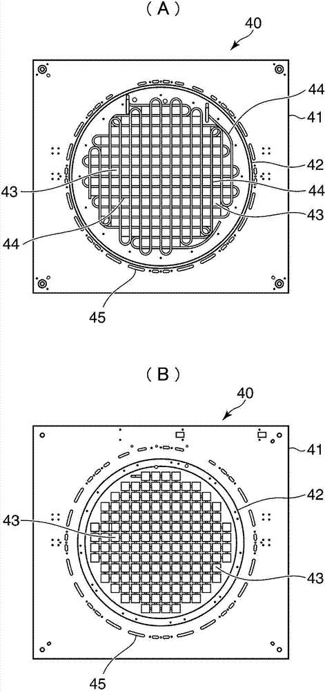
图4是表示图3的弹簧框架40的图,图4(A)是表示表面的俯视图,图4(B)是表示背面的仰视图。FIG. 4 is a view showing the
在图4(A)、(B)中,弹簧框架40主要包括:框架主体41;抵接区域42,其形成于该框架主体41的中央部,与探针卡20抵接;和设置于该抵接区域42的多个贯通孔43。弹簧框架主体41例如为因瓦合金(invar)等的低热膨胀材料制成,呈450mm×500mm的长方形的板状体,其厚度例如为10mm。中央部的抵接区域42为300mmφ的圆形区域,例如一个边长为16.5mm的正方形的贯通孔43有规律地形成有多个。贯通孔43用于使弹簧针嵌入。In Fig. 4 (A), (B), the
在图4(A)中,以沿着正方形的贯通孔43的各边的方式呈格子状地配置有作为加热装置的线状加热器44。作为线状加热器44,例如能够适当使用护套加热器(sheath heater)。护套加热器是将发热线圈插入金属、例如不锈钢制的截面2mmφ的管的中心,用MgO粉末填充固定管与发热线圈的间隙而形成的直管状的加热器,是能够进行弯曲加工,寿命长的加热器。In FIG. 4(A) ,
在抵接区域42的周围,为了降低热损失而形成有多个隔热用的贯通孔45。贯通孔45在弹簧框架主体41的厚度方向上贯通该弹簧框架主体41,降低热传导导致的热损失。A plurality of through-
设置于弹簧框架40的线状加热器(以下称为“护套加热器”)44用于对与弹簧框架40抵接的探针卡20进行加热,在其截面图中,优选设置于靠近弹簧框架40与探针卡20的抵接面的位置。由此,护套加热器44的导热效率提高,以短时间将探针卡20加热到例如与晶片W的电特性检查温度相同的温度,能够使形成于晶片W的半导体器件的电极位置、与设置与探针卡20的各探针25的位置匹配。The linear heater (hereinafter referred to as "sheath heater") 44 provided on the
图5是表示图3的晶片检查用接口装置的部分放大截面图。FIG. 5 is a partially enlarged cross-sectional view showing the interface device for wafer inspection in FIG. 3 .
在图5中,晶片检查用接口装置18主要包括:在与晶片W相对的面具备多个探针25的探针卡20;夹着晶片W与探针卡20相对配置的台状的吸盘头23;和弹簧框架40,其与探针卡20的与晶片W相对的面的相反侧的面抵接支承该探针卡20。In FIG. 5 , the
在弹簧框架40的弹簧框架主体41,设置有多个弹簧针用的贯通孔43。弹簧针用的贯通孔43例如为截面正方形的贯通孔,沿着该贯通孔43的各边例如呈格子状地设置有护套加热器44(参照图4)。如图6所示,在各贯通孔43分别嵌入有弹簧针45的凸部45A,该弹簧针45包括截面为正方形的四棱柱状的凸部45A和形成在该凸部45A的周围的台阶部45B。弹簧针45将探针卡20和设置于封头19上的省略图示的检查装置电连接。The spring frame
返回图5,探针卡20,在与晶片W相对的面具有与形成于晶片W的各半导体器件的电极对应配置的多个探针(检查针)25。另外,固定环21以包围探针卡20的形成有探针25的抵接区域42的方式形成,将探针卡20固定于弹簧框架40。Returning to FIG. 5 , the
此外,在探针卡20与晶片W之间形成有内侧空间28,在吸盘头23与固定环21之间形成有包含内侧空间28的外侧空间27。内侧空间28和外侧空间27分别通过密封材料26和24被密封(参照图3)。Furthermore, an
以下,对于利用具备上述这样的结构的晶片检查用接口装置的晶片检查装置进行的形成于晶片的半导体器件的电特性检查加以说明。Hereinafter, an electrical characteristic inspection of a semiconductor device formed on a wafer using a wafer inspection apparatus including the wafer inspection interface device having the above-mentioned structure will be described.
图7和图8是利用具备图5的晶片检查用接口装置的晶片检查装置进行的形成于晶片的半导体器件的电特性检查的工序图。7 and 8 are process diagrams of inspection of electrical characteristics of semiconductor devices formed on a wafer by the wafer inspection apparatus including the interface device for wafer inspection of FIG. 5 .
首先,作为将晶片W搬入检查室14的前处理,利用设置于弹簧框架40的护套加热器44,将与该弹簧框架40抵接的探针卡20预先加热到晶片W的特性检查温度、例如90℃。护套加热器44沿着弹簧框架40的贯通孔43的各边设置为格子状,并且设置在弹簧框架40与探针卡20的抵接面的附近,因此高效率地对探针卡20进行加热。First, as a pre-processing for carrying the wafer W into the
接着,通过晶片搬送机构13将晶片W搬入检查室14内。即,晶片搬送机构13相对于该晶片搬送机构13的拾取器13B进行校准,并且将通过内置于拾取器13B的导热加热器13C被加热到特性检查温度、例如90℃的晶片W向检查室14内搬入,并使其与探针卡20相对。这时,晶片搬送机构13使臂13A微小地移动,进行拾取器13B与探针卡20的校准(图7(A))。由此,进行晶片W与探针卡20的校准。Next, the wafer W is carried into the
接着,晶片搬送机构13使拾取器13B朝向探针卡20移动,将晶片W向探针卡20抵接。这时,已经进行了晶片W与探针卡20的校准,并且晶片W和探针卡20均被调整到晶片W的特性检查温度、即例如90℃,因此,使探针卡20的各探针25与形成于晶片W的各半导体器件的电极准确地抵接(图7(B))。在探针卡20的与晶片相对面设置的各探针25,在常温下被预先偏置地配置,使得例如在90℃探针卡20热膨胀时,分别与该被加热到90℃的热膨胀的晶片W的半导体器件的对应电极抵接。Next, the
接着,对形成于探针卡20与晶片W之间的内侧空间28进行减压,将晶片W向探针卡20吸引并临时固定,然后,拾取器13B从晶片W分离,通过晶片搬送机构13从检查室14退出(图7(C))。Next, the
接着,支承吸盘头23的升降杆22使吸盘头23向上方移动使吸盘头23与固定环21抵接。这时,吸盘头23的凸部23A从台阶部23B向上方突出,因此作为该凸部23A的上部平面的晶片载置面23C与被向探针卡20临时固定的晶片W抵接,结果是,晶片W位于晶片载置面23C上(图8(A))。Next, the lifting
接着,吸盘头23被向固定环21抵接,对吸盘头23与固定环21之间形成的外侧空间27减压,将吸盘头23向固定环21吸引,吸盘头23通过固定环21被间接地保持。这时,被向固定环21吸引的吸盘头23将位于晶片载置面23C上的晶片W向探针卡20按压,由于吸盘头23具有比晶片W高的刚性,所以能够将晶片W向探针卡20均匀地按压。然后,升降杆22向图中下方移动与吸盘头23分离(图8(B))。Then, the
接着,规定值的电流从探针卡20的各探针25向各半导体器件的电极流动,各半导体器件的电特性检查被一并进行,然后结束本检查。Next, a predetermined value of current flows from each
依据本实施方式,由于在与探针卡20的与晶片W相对的面的相反侧的面抵接而支承该探针卡20的弹簧框架40,设置有护套加热器44,因此预先利用护套加热器44将探针卡20加热到半导体器件的电特性检查温度,由此,通过使用具备多个探针25的探针卡20,该多个探针25以当被加热到该热性检查温度时,分别与被加热到该特性检查温度的晶片的半导体器件的各电极抵接的方式被配置,能够准确地将晶片W的半导体器件的电极位置与探针卡20的各探针位置对位,进而能够对形成于晶片W的半导体器件进行适当的电特性检查。另外,由于在探针卡20与晶片W抵接之前预先将晶片W向特性检查温度加热,因此当探针卡20的探针25与形成于晶片W的半导体器件抵接之后,能够防止进一步被加热而移动到电极位置,能够防止不良产品的产生。According to the present embodiment, since the
另外,依据本实施方式,由于护套加热器44为线状加热器,因此能够将该护套加热器44沿着贯通孔43的各边均匀地配置为格子状。因此,能够将探针卡20均匀地加热。In addition, according to the present embodiment, since the
在本实施方式中,设置于晶片W的半导体器件的电特性检查温度例如为50℃~150℃,优选为60~90℃。如果温度过高,则存在密封部件等中不能保持耐热性的情况。另外,如果温度过低,则不能得到作为加热部件的护套加热器44的实际效力。In this embodiment, the electrical characteristic inspection temperature of the semiconductor device provided on the wafer W is, for example, 50°C to 150°C, preferably 60 to 90°C. If the temperature is too high, heat resistance may not be maintained in sealing members and the like. In addition, if the temperature is too low, the actual effectiveness of the
在本实施方式中,使探针卡20的各探针25一并与各自对应的晶片W的全部半导体器件的对应的全部电极抵接,进行电特性检查。由此提高半导体器件的生产性。In the present embodiment, each
此外,本实施方式的晶片检查装置,由于在检查室14以外的场所进行晶片W的校准,所以晶片W和与该晶片W抵接的探针卡20的温度管理变得重要,通过设置于弹簧框架40的护套加热器44能够将探针卡20加热到任意的温度,能够进行适当的温度管理。In addition, in the wafer inspection apparatus of this embodiment, since the alignment of the wafer W is performed in a place other than the
以上,关于本发明使用上述实施方式进行了说明,但本发明并不被限定于上述的实施方式。As mentioned above, although this invention was demonstrated using the said embodiment, this invention is not limited to the said embodiment.
Claims (9)
Applications Claiming Priority (2)
| Application Number | Priority Date | Filing Date | Title |
|---|---|---|---|
| JP2012-052914 | 2012-03-09 | ||
| JP2012052914A JP6031238B2 (en) | 2012-03-09 | 2012-03-09 | Wafer inspection interface and wafer inspection apparatus |
Publications (2)
| Publication Number | Publication Date |
|---|---|
| CN103308845A true CN103308845A (en) | 2013-09-18 |
| CN103308845B CN103308845B (en) | 2015-12-02 |
Family
ID=49113545
Family Applications (1)
| Application Number | Title | Priority Date | Filing Date |
|---|---|---|---|
| CN201310074078.3A Active CN103308845B (en) | 2012-03-09 | 2013-03-08 | Wafer inspection interface arrangement and wafer inspector |
Country Status (5)
| Country | Link |
|---|---|
| US (1) | US9395405B2 (en) |
| JP (1) | JP6031238B2 (en) |
| KR (1) | KR101394354B1 (en) |
| CN (1) | CN103308845B (en) |
| TW (1) | TWI567399B (en) |
Cited By (2)
| Publication number | Priority date | Publication date | Assignee | Title |
|---|---|---|---|---|
| CN107526018A (en) * | 2016-06-21 | 2017-12-29 | 日本麦可罗尼克斯股份有限公司 | Probe card, check device and inspection method using the probe card |
| CN114487789A (en) * | 2022-04-02 | 2022-05-13 | 浙江清华柔性电子技术研究院 | Wafer detection probe and wafer detection system |
Families Citing this family (10)
| Publication number | Priority date | Publication date | Assignee | Title |
|---|---|---|---|---|
| DE602006019230D1 (en) | 2006-07-20 | 2011-02-10 | Research In Motion Ltd | Apparatus and method for supplying equipment certificates |
| JP2015529964A (en) * | 2013-04-22 | 2015-10-08 | ▲華▼▲為▼▲終▼端有限公司 | Device for preventing deformation of communication card |
| US11175309B2 (en) * | 2014-12-24 | 2021-11-16 | Qualitau, Inc. | Semi-automatic prober |
| TWI603096B (en) * | 2015-06-19 | 2017-10-21 | Seiko Epson Corp | Electronic parts conveying apparatus and electronic parts inspection apparatus |
| JP6625423B2 (en) * | 2015-12-17 | 2019-12-25 | 東京エレクトロン株式会社 | Wafer inspection apparatus and its maintenance method |
| US11280827B2 (en) * | 2016-02-29 | 2022-03-22 | Teradyne, Inc. | Thermal control of a probe card assembly |
| US11075129B2 (en) * | 2016-08-08 | 2021-07-27 | Semiconductor Components Industries, Llc | Substrate processing carrier |
| US11366156B2 (en) * | 2019-01-24 | 2022-06-21 | Stmicroelectronics Pte Ltd | Crack detection integrity check |
| JP2020074496A (en) * | 2020-02-17 | 2020-05-14 | 株式会社東京精密 | Prober |
| KR102798294B1 (en) * | 2022-09-14 | 2025-04-23 | (주)보다솔루션 | Apparatus for inspecting stiffeners for flexible displays |
Citations (6)
| Publication number | Priority date | Publication date | Assignee | Title |
|---|---|---|---|---|
| US6580282B1 (en) * | 1998-07-03 | 2003-06-17 | Stmicroelectronics S.A. | Machine for testing electronic chips |
| CN1575514A (en) * | 2001-11-30 | 2005-02-02 | 东京毅力科创株式会社 | Reliability evaluation test device, reliability evaluation test system, contactor, and reliability evaluation test method |
| JP2007208138A (en) * | 2006-02-03 | 2007-08-16 | Mitsumi Electric Co Ltd | Inspection method of semiconductor device |
| TW200823472A (en) * | 2006-11-21 | 2008-06-01 | Shinko Electric Ind Co | Probe device |
| CN101276771A (en) * | 2007-03-29 | 2008-10-01 | 东京毅力科创株式会社 | Conveyor and inspection device for the object to be inspected |
| CN102301462A (en) * | 2009-02-12 | 2011-12-28 | 株式会社爱德万测试 | Semiconductor Wafer Testing Apparatus |
Family Cites Families (11)
| Publication number | Priority date | Publication date | Assignee | Title |
|---|---|---|---|---|
| JPH06349909A (en) * | 1993-06-14 | 1994-12-22 | Hitachi Ltd | Probe inspection equipment |
| JP2000138268A (en) * | 1998-11-04 | 2000-05-16 | Hitachi Chem Co Ltd | Inspection method and inspection device of semiconductor circuit |
| JP4548817B2 (en) | 2002-10-18 | 2010-09-22 | 東京エレクトロン株式会社 | Probe device |
| JP2004363085A (en) * | 2003-05-09 | 2004-12-24 | Ebara Corp | Inspection apparatus by charged particle beam and method for manufacturing device using inspection apparatus |
| JP4308749B2 (en) * | 2004-12-08 | 2009-08-05 | 株式会社日本マイクロニクス | Prober |
| US7285968B2 (en) * | 2005-04-19 | 2007-10-23 | Formfactor, Inc. | Apparatus and method for managing thermally induced motion of a probe card assembly |
| JP5377915B2 (en) * | 2008-09-30 | 2013-12-25 | 東京エレクトロン株式会社 | Inspection apparatus and inspection method |
| JP5535492B2 (en) * | 2009-02-12 | 2014-07-02 | ラピスセミコンダクタ株式会社 | Semiconductor integrated circuit inspection apparatus and semiconductor integrated circuit inspection method |
| JP5294954B2 (en) * | 2009-04-07 | 2013-09-18 | 株式会社日本マイクロニクス | Probe card manufacturing method |
| US8400173B2 (en) * | 2009-06-26 | 2013-03-19 | Formfactor, Inc. | Method and apparatus for thermally conditioning probe cards |
| JP5629545B2 (en) * | 2009-12-18 | 2014-11-19 | 株式会社日本マイクロニクス | Probe card and inspection device |
-
2012
- 2012-03-09 JP JP2012052914A patent/JP6031238B2/en active Active
-
2013
- 2013-03-05 KR KR1020130023287A patent/KR101394354B1/en active Active
- 2013-03-07 US US13/787,956 patent/US9395405B2/en active Active
- 2013-03-08 CN CN201310074078.3A patent/CN103308845B/en active Active
- 2013-03-08 TW TW102108222A patent/TWI567399B/en not_active IP Right Cessation
Patent Citations (6)
| Publication number | Priority date | Publication date | Assignee | Title |
|---|---|---|---|---|
| US6580282B1 (en) * | 1998-07-03 | 2003-06-17 | Stmicroelectronics S.A. | Machine for testing electronic chips |
| CN1575514A (en) * | 2001-11-30 | 2005-02-02 | 东京毅力科创株式会社 | Reliability evaluation test device, reliability evaluation test system, contactor, and reliability evaluation test method |
| JP2007208138A (en) * | 2006-02-03 | 2007-08-16 | Mitsumi Electric Co Ltd | Inspection method of semiconductor device |
| TW200823472A (en) * | 2006-11-21 | 2008-06-01 | Shinko Electric Ind Co | Probe device |
| CN101276771A (en) * | 2007-03-29 | 2008-10-01 | 东京毅力科创株式会社 | Conveyor and inspection device for the object to be inspected |
| CN102301462A (en) * | 2009-02-12 | 2011-12-28 | 株式会社爱德万测试 | Semiconductor Wafer Testing Apparatus |
Cited By (2)
| Publication number | Priority date | Publication date | Assignee | Title |
|---|---|---|---|---|
| CN107526018A (en) * | 2016-06-21 | 2017-12-29 | 日本麦可罗尼克斯股份有限公司 | Probe card, check device and inspection method using the probe card |
| CN114487789A (en) * | 2022-04-02 | 2022-05-13 | 浙江清华柔性电子技术研究院 | Wafer detection probe and wafer detection system |
Also Published As
| Publication number | Publication date |
|---|---|
| US9395405B2 (en) | 2016-07-19 |
| CN103308845B (en) | 2015-12-02 |
| TW201403089A (en) | 2014-01-16 |
| KR20130103379A (en) | 2013-09-23 |
| KR101394354B1 (en) | 2014-05-13 |
| TWI567399B (en) | 2017-01-21 |
| JP2013187457A (en) | 2013-09-19 |
| US20130234745A1 (en) | 2013-09-12 |
| JP6031238B2 (en) | 2016-11-24 |
Similar Documents
| Publication | Publication Date | Title |
|---|---|---|
| CN103308845B (en) | Wafer inspection interface arrangement and wafer inspector | |
| JP5489356B2 (en) | Semiconductor measuring equipment | |
| US20130241588A1 (en) | Wafer inspection apparatus | |
| JP6782103B2 (en) | Probe card, inspection equipment and inspection method | |
| CN104181449B (en) | Test equipment and correlation technique | |
| KR101406753B1 (en) | Wafer inspection interface and wafer inspection apparatus | |
| TW200907359A (en) | Electrical signal connector | |
| KR102014334B1 (en) | Cartridge for inspecting substrates and manufacturing method thereof | |
| JP7153556B2 (en) | Temperature measurement member, inspection device and temperature measurement method | |
| CN108470690B (en) | detector | |
| JP5546328B2 (en) | Wafer test method and prober | |
| KR102268438B1 (en) | Inspection apparatus and inspection method | |
| CN110716123B (en) | Intermediate connecting member and inspection device | |
| JP6685526B1 (en) | Prober device and measuring jig | |
| JP2020047860A (en) | Inspection device and inspection method | |
| CN119856264A (en) | Temperature measurement substrate calibration method, substrate temperature measurement system and temperature measurement substrate |
Legal Events
| Date | Code | Title | Description |
|---|---|---|---|
| C06 | Publication | ||
| PB01 | Publication | ||
| C10 | Entry into substantive examination | ||
| SE01 | Entry into force of request for substantive examination | ||
| C14 | Grant of patent or utility model | ||
| GR01 | Patent grant |