CN103295629A - Method for improving write cycle speed of phase change memory unit - Google Patents
Method for improving write cycle speed of phase change memory unit Download PDFInfo
- Publication number
- CN103295629A CN103295629A CN 201210044892 CN201210044892A CN103295629A CN 103295629 A CN103295629 A CN 103295629A CN 201210044892 CN201210044892 CN 201210044892 CN 201210044892 A CN201210044892 A CN 201210044892A CN 103295629 A CN103295629 A CN 103295629A
- Authority
- CN
- China
- Prior art keywords
- set operation
- reset operation
- change memory
- reset
- write
- Prior art date
- Legal status (The legal status is an assumption and is not a legal conclusion. Google has not performed a legal analysis and makes no representation as to the accuracy of the status listed.)
- Pending
Links
- 238000000034 method Methods 0.000 title claims abstract description 51
- 230000008859 change Effects 0.000 title abstract description 4
- 230000008569 process Effects 0.000 claims abstract description 28
- 238000002425 crystallisation Methods 0.000 abstract description 7
- 230000008025 crystallization Effects 0.000 abstract description 7
- 238000002679 ablation Methods 0.000 description 17
- 230000007704 transition Effects 0.000 description 9
- 238000010586 diagram Methods 0.000 description 6
- 230000008901 benefit Effects 0.000 description 3
- 239000000463 material Substances 0.000 description 3
- 239000012782 phase change material Substances 0.000 description 3
- 238000010438 heat treatment Methods 0.000 description 2
- 230000004048 modification Effects 0.000 description 2
- 238000012986 modification Methods 0.000 description 2
- 230000007423 decrease Effects 0.000 description 1
- 230000006870 function Effects 0.000 description 1
- 230000000155 isotopic effect Effects 0.000 description 1
- 239000004065 semiconductor Substances 0.000 description 1
Images


Landscapes
- Semiconductor Memories (AREA)
Abstract
The invention provides a method for improving write cycle speed of a phase change memory unit. The method comprises the following steps of: determining number m of setting operations and number n of resetting operations, wherein m and n are natural numbers; and dividing into three different write modes according to the condition whether the number m of setting operations and number n of resetting operations are 0. According to the characteristic that the crystallization period of the setting operations is long, the resetting operations with proper number are inserted into the crystallization period of the setting operations, rapid data write can be realized through the method for overlapping the setting operations and the resetting operations, the overall write operation time is shortened, the speed of the write process is improved, the write cycle is shortened, the current stability in the write process is improved, the maximum current is controlled, the maximum allowed current in the write process is reduced, and the power consumption in the overall write operation is reduced.
Description
Technical field
The present invention relates to storer and write technical field, relate to a kind of method that improves phase-change memory cell speed write cycle especially.
Background technology
Phase transition storage (PCM) can be realized one of business-like storer of future generation at first by the prediction of international semiconductor federation.Phase transition storage with present other dynamic storagies (DRAM), flash memory (Flash) is compared has following clear superiority: one, volume is little; Two, driving voltage is low; Three, power consumption is little; Four, read or write speed is fast.In addition, phase transition storage is applicable to extreme environment, radioresistance, anti-vibration.Therefore phase transition storage has many irreplaceable application and important meaning in fields such as Aero-Space and national defence.
The principle of work of phase transition storage mainly is by applying dissimilar pulses at phase-change material, making the phase-change material regional area produce the difference of amorphous state and crystalline state because of different temperatures.Yet phase-change material is to temperature, heating current, and heat time heating time is very responsive.These several factors all may cause the ablation process of phase transition storage to consume more multiple current, expend more write times, thereby cause the slow of ablation process.Therefore improve writing speed, control writes electric current that very important meaning is arranged.
At present, Chang Yong phase transition storage ablation process as shown in Figure 1.Generally speaking, in phase transition storage, for increasing the bit that writes of data, can put into a plurality of write driver circuits, be used for carrying out the not operation of isotopic number.Therefore, the situation that set operation and reset operation carry out simultaneously can appear.Because in traditional method, set operation or reset operation all are continuous execution, so that maximum current can control in lower scope, thereby save power consumption.Because the crystallization time that the process need of set operation is long, therefore the decline process of electric current is slower, be several times of reset operation required time, therefore set operation is more many, then the write time also can be more long, simultaneously, owing to can not effectively utilize during this period of time, cause write cycle longer at interval, reduced the efficient that writes of phase transition storage.If but there are set and reset operation to carry out simultaneously, then overall current can be bigger, and power consumption raises.
Summary of the invention
The present invention is intended to solve at least the technical matters that exists in the prior art, has proposed to special innovation a kind of method that improves phase-change memory cell speed write cycle.
In order to realize above-mentioned purpose of the present invention, the invention provides a kind of method that improves phase-change memory cell speed write cycle, it comprises the steps:
S1: determine the number m of set operation and the number n of reset operation, described m, n are natural number;
S2: the numerical value according to the number n of the number m of set operation and reset operation carries out set operation and reset operation, is specially:
S21: if the number n of the number m of set operation and reset operation is 0, then finish write operation;
S22: if the number m of set operation is not 0, the number n of reset operation is 0, then carries out the set operation of a position simultaneously, and described a is positive integer, after the execution, makes m=m-a, continues to return execution in step S22, is 0 until m, finishes write operation;
S23: if the number m of set operation is 0, the number n of reset operation is not 0, then carries out the reset operation of b position continuously, and described b is positive integer, after the execution, makes n=n-b, continues to return execution in step S23, is 0 until n, finishes write operation;
S24: if the number m of set operation is not 0, the number n of reset operation is not 0 yet, then carry out the set operation of c position simultaneously, in the process of set operation, carry out the reset operation of d position continuously, described c and d are positive integer, after the execution, make m=m-c, make n=n-d, continue to return execution in step S24, have one to be 0 in m or n, when the number m of set operation is not 0, the number n of reset operation is 0 o'clock, return step S22, when the number m of set operation is 0, the number n of reset operation is not 0 o'clock, returns step S23.
Whether the present invention is 0 to carry out different write modes by detecting set operation number and reset operation number, the characteristics long according to the set operation crystallization time, the reset operation of proper number is inserted into the crystallization time of set operation, the overlapping method of this set operation and reset operation can realize that rapid data writes, realize the minimizing of whole write operation time, improve the speed of ablation process, shorten write cycle, and can improve the stability of electric current in the ablation process, realization is to the control of maximum current, reduce maximum allowed current in the ablation process, reduce the power consumption of whole write operation.The present invention has avoided can reducing the fluctuation of ablation process electric current to writing the wait that electric current falls after rise, the maximum current of fixing whole ablation process; Reduce the overall power of ablation process; Improve the whole efficient that writes.
Additional aspect of the present invention and advantage part in the following description provide, and part will become obviously from the following description, or recognize by practice of the present invention.
Description of drawings
Above-mentioned and/or additional aspect of the present invention and advantage are from obviously and easily understanding becoming the description of embodiment in conjunction with following accompanying drawing, wherein:
Fig. 1 is three kinds of situations that set operation and reset operation may occur in the ablation process of prior art phase-change memory cell;
Fig. 2 improves the specific implementation process flow diagram of ablation process in the method for phase-change memory cell speed write cycle for the present invention;
Fig. 3 improves electric current and the time relation synoptic diagram of ablation process in a kind of embodiment of method of phase-change memory cell speed write cycle for the present invention;
Fig. 4 improves the write mode mode of operation in a kind of embodiment of method of phase-change memory cell speed write cycle and writes the total current synoptic diagram for the present invention.
Embodiment
Describe embodiments of the invention below in detail, the example of described embodiment is shown in the drawings, and wherein identical or similar label is represented identical or similar elements or the element with identical or similar functions from start to finish.Be exemplary below by the embodiment that is described with reference to the drawings, only be used for explaining the present invention, and can not be interpreted as limitation of the present invention.
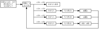
Fig. 2 is the specific implementation process flow diagram of ablation process of the present invention, and as seen from the figure, the method for this raising phase-change memory cell speed write cycle comprises the steps:
S1: determine the number m of set operation and the number n of reset operation, described m, n are natural number;
S2: the numerical value according to the number n of the number m of set operation and reset operation carries out set operation and reset operation, is specially:
S21: if the number n of the number m of set operation and reset operation is 0, then finish write operation;
S22: if the number m of set operation is not 0, the number n of reset operation is 0, then carries out write mode A, namely, carry out the set operation of a position simultaneously, described a is positive integer, after the execution, makes m=m-a, continuing to return execution in step S22, is 0 until m, finishes write operation;
S23: if the number m of set operation is 0, the number n of reset operation is not 0, then carries out write mode B, namely, carry out the reset operation of b position continuously, described b is positive integer, after the execution, makes n=n-b, continuing to return execution in step S23, is 0 until n, finishes write operation;
S24: if the number m of set operation is not 0, the number n of reset operation is not 0 yet, then carry out write mode C, that is, carry out the set operation of c position simultaneously, in the process of set operation, carry out the reset operation of d position continuously, described c and d are positive integer, after the execution, make m=m-c, make n=n-d, continue to return execution in step S 24, have one to be 0 in m or n, when the number m of set operation is not 0, the number n of reset operation is 0 o'clock, return step S22, when the number m of set operation is 0, the number n of reset operation is not 0 o'clock, returns step S23.
In the present embodiment, determine the number m of set operation and the number n of reset operation by the data that detect FPDP.
According to the characteristic of phase-change memory material, the electric current of reset operation is greater than the electric current of set operation, and the time of reset operation is shorter, and set operation is owing to the very long crystallization time of needs, so the time is longer.The electric current I of reset operation of the present invention
ResetIt is the electric current I of set operation
SetK doubly, the maximum allowed current I that phase-change memory cell writes
MaxIt is the electric current I of set operation
SetP doubly, wherein, K, P are positive number, and K≤P is arranged, in the set operation fall time of electric current be the reset operation time Q doubly, wherein, Q is the positive number greater than 1.In ablation process, the set operation figure place a≤P that carries out simultaneously, c≤P.
In a kind of preferred implementation of the present invention, in step S24, namely among the write mode C, when the electric current of set operation drops to (P-K) * I
SetCarry out reset operation when following.In a kind of embodiment that is more preferably of the present invention, when the electric current of set operation just drops to (P-K) * I
SetThe time, carry out reset operation immediately.
In the present invention, get the maximum allowed current I that phase-change memory cell writes
MaxElectric current I for set operation
SetTwice at least, i.e. P 〉=2, P neither be infinitely great certainly, reaches the standard grade for it with the maximum current that phase-change memory cell can bear.In the present embodiment, P is taken as 2, then a can get 1 or 2, c also can get 1 or 2, in the present embodiment, get a=2, c=2.
In the present embodiment, get electric current in the reset operation and be electric current in the set operation 1.5 times, i.e. K=1.5, be 6 times of set operation time the fall time of electric current in the reset operation, be Q=6, the electric current of concrete ablation process and time relationship synoptic diagram are as shown in Figure 3.Fig. 4 shows the mode of operation of three kinds of write modes and writes the total current synoptic diagram.As seen from the figure, ablation process needs at first to determine the number m of set operation and the number n of reset operation, numerical value according to the number n of the number m of set operation and reset operation carries out three kinds of write modes then, if detect and do not have reset operation, be n=0, and m set operation arranged, then enter write mode A, namely carry out the set operation of 2 positions simultaneously, because the set operation of 2 positions is carried out simultaneously, the set operation of 2 positions overlaps in Fig. 4 (a), and the maximum current that carries out the set operation generation of 2 positions shown in Fig. 4 (b) simultaneously is 2 times set operation electric current I
Set, the set operation number becomes m-2 then, continues execution pattern A, is 0 until m, finishes write operation.There is not set operation if detect, i.e. m=0, and n reset operation arranged, and then enter write mode B, carry out the reset operation of b position continuously, described b is positive integer, and in the present embodiment, b is taken as 3, and the maximum current of generation is 1.5 times set operation electric current I
Set, the reset operation number becomes n-3 then, continues execution pattern B, is 0 until n, finishes write operation.If detect m set and n reset operation are arranged simultaneously, then enter write mode C, namely carry out 2 set operation simultaneously, carry out the reset operation of d position continuously in the process of set operation, in the present embodiment, d is taken as 3.In the present embodiment, the electric current when set operation drops to 0.5 * I
SetCarry out reset operation when following.In a kind of embodiment that is more preferably of the present invention, when the electric current of set operation has just dropped to 0.5 * I
SetThe time, carry out reset operation immediately.After the execution, make m=m-2, make n=n-3, continue to carry out write mode C, in m or n, have one to be 0, when the number m of set operation is not 0, the number n of reset operation is 0 o'clock, carries out write mode A, when the number m of set operation is 0, the number n of reset operation is not 0 o'clock, carries out write mode B.
The present invention is by the switching of three kinds of write modes, and the maximum current that produces in the ablation process is 2 times set operation electric current I
SetBut in traditional method, maximum current then is 2.5 times set operation electric current I
Set, and the write time can prolong along with the increased frequency of set operation.So method of the present invention has not only effectively reduced to write in the unit interval power consumption of electric current, and be 2 times set operation electric current with the maximum current limit of integral body, improved whole writing speed, shortened write cycle.In the present invention, control different write circuits by current detector and corresponding logical circuit and carry out different write modes respectively, change by different write modes, can take full advantage of crystallization time long in the set operation, reduce whole writing current power dissipation and raising writes efficient.
The present invention is according to the maximum current that allows in the phase-change memory cell design, performed set operation and the parameter a in the reset operation among write mode A, B, the C, b, c, d can change accordingly, the numerical value that is not limited to adopt in the embodiment of the invention, by set operation and the reasonably switching of overlapping and different write modes of reset operation, to adapt to the demand of different designs, can improve the whole efficient that writes, the whole maximum of control writes strength of current and shortens write cycle.
In addition, the present invention is not only applicable to the writing of single storage unit, and is same for writing of logical memory blocks yet, and this also should be included within protection scope of the present invention.
In the description of this instructions, concrete feature, structure, material or characteristics that the description of reference term " embodiment ", " some embodiment ", " example ", " concrete example " or " some examples " etc. means in conjunction with this embodiment or example description are contained at least one embodiment of the present invention or the example.In this manual, the schematic statement to above-mentioned term not necessarily refers to identical embodiment or example.And concrete feature, structure, material or the characteristics of description can be with the suitable manner combination in any one or more embodiment or example.
Although illustrated and described embodiments of the invention, those having ordinary skill in the art will appreciate that: can carry out multiple variation, modification, replacement and modification to these embodiment under the situation that does not break away from principle of the present invention and aim, scope of the present invention is limited by claim and equivalent thereof.
Claims (7)
1. a method that improves phase-change memory cell speed write cycle is characterized in that, comprises the steps:
S1: determine the number m of set operation and the number n of reset operation, described m, n are natural number;
S2: the numerical value according to the number n of the number m of set operation and reset operation carries out set operation and reset operation, is specially:
S21: if the number n of the number m of set operation and reset operation is 0, then finish write operation;
S22: if the number m of set operation is not 0, the number n of reset operation is 0, then carries out the set operation of a position simultaneously, and described a is positive integer, after the execution, makes m=m-a, continues to return execution in step S22, is 0 until m, finishes write operation;
S23: if the number m of set operation is 0, the number n of reset operation is not 0, then carries out the reset operation of b position continuously, and described b is positive integer, after the execution, makes n=n-b, continues to return execution in step S23, is 0 until n, finishes write operation;
S24: if the number m of set operation is not 0, the number n of reset operation is not 0 yet, then carry out the set operation of c position simultaneously, in the process of set operation, carry out the reset operation of d position continuously, described c and d are positive integer, after the execution, make m=m-c, make n=n-d, continue to return execution in step S24, have one to be 0 in m or n, when the number m of set operation is not 0, the number n of reset operation is 0 o'clock, return step S22, when the number m of set operation is 0, the number n of reset operation is not 0 o'clock, returns step S23.
2. the method for raising phase-change memory cell speed write cycle as claimed in claim 1 is characterized in that, the electric current I of described reset operation
ResetIt is the electric current I of set operation
SetK doubly, the maximum allowed current I that described phase-change memory cell writes
MaxElectric current I for set operation
SetP doubly, described K, P are positive number, described K≤P.
3. the method for raising phase-change memory cell speed write cycle as claimed in claim 1 or 2 is characterized in that, described a≤P, described c≤P.
4. the method for raising phase-change memory cell speed write cycle as claimed in claim 1 or 2 is characterized in that, in step S24, when the electric current of set operation drops to (P-K) * I
SetCarry out reset operation when following.
5. as the method for claim 1,2, one of 4 described raising phase-change memory cell speed write cycle, it is characterized in that, in step S24, when the electric current of set operation drops to (P-K) * I
SetThe Shi Jinhang reset operation.
6. as the method for claim 2,3,4, one of 5 described raising phase-change memory cell speed write cycle, it is characterized in that described P 〉=2.
7. the method for raising phase-change memory cell speed write cycle as claimed in claim 1 is characterized in that, in the described set operation fall time of electric current be the reset operation time Q doubly, described Q is the positive number greater than 1.
Priority Applications (1)
| Application Number | Priority Date | Filing Date | Title |
|---|---|---|---|
| CN 201210044892 CN103295629A (en) | 2012-02-22 | 2012-02-22 | Method for improving write cycle speed of phase change memory unit |
Applications Claiming Priority (1)
| Application Number | Priority Date | Filing Date | Title |
|---|---|---|---|
| CN 201210044892 CN103295629A (en) | 2012-02-22 | 2012-02-22 | Method for improving write cycle speed of phase change memory unit |
Publications (1)
| Publication Number | Publication Date |
|---|---|
| CN103295629A true CN103295629A (en) | 2013-09-11 |
Family
ID=49096358
Family Applications (1)
| Application Number | Title | Priority Date | Filing Date |
|---|---|---|---|
| CN 201210044892 Pending CN103295629A (en) | 2012-02-22 | 2012-02-22 | Method for improving write cycle speed of phase change memory unit |
Country Status (1)
| Country | Link |
|---|---|
| CN (1) | CN103295629A (en) |
Cited By (2)
| Publication number | Priority date | Publication date | Assignee | Title |
|---|---|---|---|---|
| CN104882161A (en) * | 2014-02-28 | 2015-09-02 | 复旦大学 | Resistive random access memory and write operation method thereof |
| CN105304128A (en) * | 2014-07-15 | 2016-02-03 | 旺宏电子股份有限公司 | Method for storing data value in memory cell and memory |
-
2012
- 2012-02-22 CN CN 201210044892 patent/CN103295629A/en active Pending
Cited By (3)
| Publication number | Priority date | Publication date | Assignee | Title |
|---|---|---|---|---|
| CN104882161A (en) * | 2014-02-28 | 2015-09-02 | 复旦大学 | Resistive random access memory and write operation method thereof |
| CN104882161B (en) * | 2014-02-28 | 2017-07-11 | 复旦大学 | A kind of resistor-type random-access memory and its write operation method |
| CN105304128A (en) * | 2014-07-15 | 2016-02-03 | 旺宏电子股份有限公司 | Method for storing data value in memory cell and memory |
Similar Documents
| Publication | Publication Date | Title |
|---|---|---|
| CN103915110B (en) | Refreshing method of volatile memory and related controller of volatile memory | |
| US8644061B2 (en) | Variable resistance memory device performing program and verification operation | |
| US9142263B2 (en) | Power management control and controlling memory refresh operations | |
| US8917568B2 (en) | Method of operating PSRAM and related memory device | |
| US9984737B2 (en) | Reduction of power consumption in memory devices during refresh modes | |
| KR102011796B1 (en) | Memory device and memory system including the same | |
| KR100909630B1 (en) | Address counter circuit | |
| KR20170045795A (en) | Memory device and memory system including the same | |
| JP2013524401A (en) | How to program memory using variable data width | |
| US9460778B2 (en) | Static random access memory with bitline boost | |
| CN103544987B (en) | Semiconductor memory element with self-refresh sequential circuit | |
| EP3063767B1 (en) | Write pulse width scheme in a resistive memory | |
| CN102270505A (en) | Phase change storage unit and phase change memory | |
| US7746718B2 (en) | Semiconductor memory, operating method of semiconductor memory, memory controller, and system | |
| CN102592665A (en) | High-speed data writing structure and writing method for phase change memory | |
| CN101471130B (en) | Phase change memory and control method of phase change memory | |
| WO2015088740A1 (en) | Refresh scheme for memory cells with next bit table | |
| WO2009061532A1 (en) | Voltage-stepped low-power memory device | |
| CN103295629A (en) | Method for improving write cycle speed of phase change memory unit | |
| US9666297B1 (en) | Memory device, memory system including the same and operation method of the memory system | |
| US8266464B2 (en) | Power controller, a method of operating the power controller and a semiconductor memory system employing the same | |
| US20150316971A1 (en) | Method and apparatus to reduce power consumption of mobile and portable devices with non-volatile memories | |
| CN105632546A (en) | MRAM (Magnetic Random Access Memory) chip and self-refreshing operation method thereof | |
| KR20240173350A (en) | Semiconductor device | |
| CN102592672A (en) | Flash electrically erasable programmable read-only memory (EEPROM) dynamic reference resource circuit structure |
Legal Events
| Date | Code | Title | Description |
|---|---|---|---|
| C06 | Publication | ||
| PB01 | Publication | ||
| C10 | Entry into substantive examination | ||
| SE01 | Entry into force of request for substantive examination | ||
| C02 | Deemed withdrawal of patent application after publication (patent law 2001) | ||
| WD01 | Invention patent application deemed withdrawn after publication |
Application publication date: 20130911 |