CN103014644A - ITO (indium tin oxide) film for touch screen and preparation method thereof - Google Patents
ITO (indium tin oxide) film for touch screen and preparation method thereof Download PDFInfo
- Publication number
- CN103014644A CN103014644A CN2012105650971A CN201210565097A CN103014644A CN 103014644 A CN103014644 A CN 103014644A CN 2012105650971 A CN2012105650971 A CN 2012105650971A CN 201210565097 A CN201210565097 A CN 201210565097A CN 103014644 A CN103014644 A CN 103014644A
- Authority
- CN
- China
- Prior art keywords
- preparation
- film
- touch
- ito film
- magnetron sputtering
- Prior art date
- Legal status (The legal status is an assumption and is not a legal conclusion. Google has not performed a legal analysis and makes no representation as to the accuracy of the status listed.)
- Pending
Links
- 238000002360 preparation method Methods 0.000 title claims abstract description 19
- AMGQUBHHOARCQH-UHFFFAOYSA-N indium;oxotin Chemical compound [In].[Sn]=O AMGQUBHHOARCQH-UHFFFAOYSA-N 0.000 title abstract description 4
- 238000001755 magnetron sputter deposition Methods 0.000 claims abstract description 32
- 239000010410 layer Substances 0.000 claims abstract description 31
- XKRFYHLGVUSROY-UHFFFAOYSA-N Argon Chemical compound [Ar] XKRFYHLGVUSROY-UHFFFAOYSA-N 0.000 claims abstract description 24
- 239000002344 surface layer Substances 0.000 claims abstract description 21
- IJGRMHOSHXDMSA-UHFFFAOYSA-N Atomic nitrogen Chemical compound N#N IJGRMHOSHXDMSA-UHFFFAOYSA-N 0.000 claims abstract description 14
- 229910052786 argon Inorganic materials 0.000 claims abstract description 12
- 239000013077 target material Substances 0.000 claims abstract description 11
- QVGXLLKOCUKJST-UHFFFAOYSA-N atomic oxygen Chemical compound [O] QVGXLLKOCUKJST-UHFFFAOYSA-N 0.000 claims abstract description 9
- 239000001301 oxygen Substances 0.000 claims abstract description 9
- 229910052760 oxygen Inorganic materials 0.000 claims abstract description 9
- 229910052757 nitrogen Inorganic materials 0.000 claims abstract description 7
- 239000007789 gas Substances 0.000 claims description 26
- 230000015572 biosynthetic process Effects 0.000 claims description 21
- 238000004544 sputter deposition Methods 0.000 claims description 18
- 239000011159 matrix material Substances 0.000 claims description 9
- 239000000203 mixture Substances 0.000 claims description 8
- PJXISJQVUVHSOJ-UHFFFAOYSA-N indium(iii) oxide Chemical compound [O-2].[O-2].[O-2].[In+3].[In+3] PJXISJQVUVHSOJ-UHFFFAOYSA-N 0.000 claims description 6
- 238000000034 method Methods 0.000 claims description 6
- XOLBLPGZBRYERU-UHFFFAOYSA-N tin dioxide Chemical compound O=[Sn]=O XOLBLPGZBRYERU-UHFFFAOYSA-N 0.000 claims description 6
- MRNHPUHPBOKKQT-UHFFFAOYSA-N indium;tin;hydrate Chemical group O.[In].[Sn] MRNHPUHPBOKKQT-UHFFFAOYSA-N 0.000 claims description 4
- -1 polyethylene terephthalate Polymers 0.000 claims description 4
- 229910004298 SiO 2 Inorganic materials 0.000 claims description 3
- 150000002466 imines Chemical class 0.000 claims description 3
- 229920000139 polyethylene terephthalate Polymers 0.000 claims description 3
- 239000005020 polyethylene terephthalate Substances 0.000 claims description 3
- 239000002356 single layer Substances 0.000 claims description 3
- 239000000758 substrate Substances 0.000 abstract description 6
- 238000005516 engineering process Methods 0.000 abstract description 3
- 238000004519 manufacturing process Methods 0.000 abstract description 3
- 238000010924 continuous production Methods 0.000 abstract 1
- 238000009776 industrial production Methods 0.000 abstract 1
- 239000013076 target substance Substances 0.000 abstract 1
- 239000010408 film Substances 0.000 description 21
- 239000010409 thin film Substances 0.000 description 6
- 238000000576 coating method Methods 0.000 description 5
- XUIMIQQOPSSXEZ-UHFFFAOYSA-N Silicon Chemical compound [Si] XUIMIQQOPSSXEZ-UHFFFAOYSA-N 0.000 description 4
- XLOMVQKBTHCTTD-UHFFFAOYSA-N Zinc monoxide Chemical compound [Zn]=O XLOMVQKBTHCTTD-UHFFFAOYSA-N 0.000 description 4
- 239000011248 coating agent Substances 0.000 description 4
- 239000000463 material Substances 0.000 description 4
- 239000010703 silicon Substances 0.000 description 4
- 238000004804 winding Methods 0.000 description 4
- 238000005452 bending Methods 0.000 description 3
- 238000010438 heat treatment Methods 0.000 description 3
- 238000005096 rolling process Methods 0.000 description 3
- 229910052710 silicon Inorganic materials 0.000 description 3
- VVTSZOCINPYFDP-UHFFFAOYSA-N [O].[Ar] Chemical compound [O].[Ar] VVTSZOCINPYFDP-UHFFFAOYSA-N 0.000 description 2
- 238000001514 detection method Methods 0.000 description 2
- 229910001882 dioxygen Inorganic materials 0.000 description 2
- 238000005530 etching Methods 0.000 description 2
- 239000010955 niobium Substances 0.000 description 2
- 229910000484 niobium oxide Inorganic materials 0.000 description 2
- URLJKFSTXLNXLG-UHFFFAOYSA-N niobium(5+);oxygen(2-) Chemical group [O-2].[O-2].[O-2].[O-2].[O-2].[Nb+5].[Nb+5] URLJKFSTXLNXLG-UHFFFAOYSA-N 0.000 description 2
- TWNQGVIAIRXVLR-UHFFFAOYSA-N oxo(oxoalumanyloxy)alumane Chemical compound O=[Al]O[Al]=O TWNQGVIAIRXVLR-UHFFFAOYSA-N 0.000 description 2
- 238000005057 refrigeration Methods 0.000 description 2
- 238000012360 testing method Methods 0.000 description 2
- XLYOFNOQVPJJNP-UHFFFAOYSA-N water Substances O XLYOFNOQVPJJNP-UHFFFAOYSA-N 0.000 description 2
- 239000011787 zinc oxide Substances 0.000 description 2
- 241000863032 Trieres Species 0.000 description 1
- 239000002390 adhesive tape Substances 0.000 description 1
- 230000009286 beneficial effect Effects 0.000 description 1
- 230000005540 biological transmission Effects 0.000 description 1
- 238000002425 crystallisation Methods 0.000 description 1
- 230000008025 crystallization Effects 0.000 description 1
- 230000007547 defect Effects 0.000 description 1
- 238000005137 deposition process Methods 0.000 description 1
- 238000010586 diagram Methods 0.000 description 1
- 230000004907 flux Effects 0.000 description 1
- 239000011521 glass Substances 0.000 description 1
- RHZWSUVWRRXEJF-UHFFFAOYSA-N indium tin Chemical compound [In].[Sn] RHZWSUVWRRXEJF-UHFFFAOYSA-N 0.000 description 1
- 238000009413 insulation Methods 0.000 description 1
- 238000007733 ion plating Methods 0.000 description 1
- 229910052751 metal Inorganic materials 0.000 description 1
- 239000002184 metal Substances 0.000 description 1
- 229910044991 metal oxide Inorganic materials 0.000 description 1
- 238000011056 performance test Methods 0.000 description 1
- 239000000843 powder Substances 0.000 description 1
- 238000002203 pretreatment Methods 0.000 description 1
- 238000002310 reflectometry Methods 0.000 description 1
- 239000004065 semiconductor Substances 0.000 description 1
- 229910052814 silicon oxide Inorganic materials 0.000 description 1
- 238000004381 surface treatment Methods 0.000 description 1
- 238000002834 transmittance Methods 0.000 description 1
- MEYZYGMYMLNUHJ-UHFFFAOYSA-N tunicamycin Natural products CC(C)CCCCCCCCCC=CC(=O)NC1C(O)C(O)C(CC(O)C2OC(C(O)C2O)N3C=CC(=O)NC3=O)OC1OC4OC(CO)C(O)C(O)C4NC(=O)C MEYZYGMYMLNUHJ-UHFFFAOYSA-N 0.000 description 1
Landscapes
- Physical Vapour Deposition (AREA)
Abstract
The invention relates to an ITO (indium tin oxide) film for a touch screen and a preparation method thereof, and belongs to the technical field of electronic screens. The preparation method comprises the following step: under a magnetron sputtering condition, applying a power supply to a magnetron target to sputter and deposit a target substance on a magnetron target material on a transparent substrate so as to form a film layer on the substrate, wherein the film layer comprises a bottom layer, a middle layer and a first surface layer which are sequentially arranged upwardly from the upper surface of the transparent substrate; and the film layer is formed in an argon, nitrogen and/ or oxygen atmosphere. By the preparation method, a flexible ITO film is prepared through vacuum magnetron sputtering for the first time; and the ITO film is deposited on a flexible substrate through magnetron sputtering, and then adhered to the substrate by an adhering technology and the like; therefore, the ITO film prepared by the preparation method is good in adhesion and excellent in performance, the preparation method is convenient for industrial continuous production, the production efficiency is greatly improved, and the preparation method is a first choice for industrial production.
Description
Technical field
The present invention relates to a kind of ITO film for touch-screen and preparation method thereof, belong to the technical field of electronic curtain.
Background technology
ITO(Indium Tin Oxides, indium tin metal oxide compound), be used in widely the fields such as mobile phone, MP3, MP4, digital camera as a kind of typical N-type oxide semiconductor.
The method for preparing the ITO plated film has a lot, is generally the ITO powder and ITO is deposited to the matrix surfaces such as glass, metal by vapour deposition process, forms a thin film layer.
Summary of the invention
In order to overcome defects, the object of the present invention is to provide a kind of ITO film that is used for touch-screen that is conducive to the needs that industrialization, serialization produce and preparation method thereof.
To achieve these goals, the present invention adopts following technical scheme:
A kind of ITO film for touch-screen, this film comprise transparent base and the rete that is plated on the described transparent base, and described rete comprises bottom, middle layer and the first surface layer that the self-induced transparency body upper surface is upwards arranged successively.
Described bottom, middle layer and the first surface layer are single layer structure.
The thickness of described transparent base is 50-188 μ m, and described transparent base is polyethylene terephthalate or poly-imines.
Described bottom is SiO
2Or Al
2O
3Described middle layer is Si
3N
4Or Nb
2O
5Described the first surface layer is the ITO layer.
The method is included under the magnetron sputtering condition, applying power supply at magnetic controlling target makes the target material sputter on the magnetic control target and deposits on the transparent base, to form rete at matrix, described rete comprises bottom, middle layer and the first surface layer that the self-induced transparency body upper surface is upwards arranged successively; Forming as mentioned above, rete all carries out under argon gas, nitrogen and/or oxygen atmosphere.
Wherein, under the magnetron sputtering condition, described formation underlayer thickness is 12-60nm, and described formation intermediate layer thickness is 7-10nm, and described formation first surface layer thickness is 18-29nm.
Described magnetic control target is tin indium oxide target material, and composition is the Indium sesquioxide of 95wt% and the stannic oxide of 5wt%.
The sputtering condition of described formation bottom film comprises that the power of power supply is 12-30kw, and the vacuum tightness of magnetron sputtering is 9.0E-04--1.6E-03mbar, and the flow of working gas is 260-320sccm, and sputter rate is 0.8-1.4m/min.
The sputtering condition of described formation intermediate layer film comprises the power 6-8kw of power supply, and the vacuum tightness of magnetron sputtering is 1.2E-03-1.4E-03mbar, and the flow of working gas is 90-170sccm, and sputter rate is 0.8-1.4m/min.
The sputtering condition of described formation first surface layer film comprises that the power of power supply is 4.3-7kw, and the vacuum tightness of magnetron sputtering is 2.0E-03-2.9E-03mbar, and the flow of working gas is 255-325sccm, and sputter rate is 0.8-1.4m/min.
Beneficial effect of the present invention:
The present invention takes the lead in adopting the standby flexible ito thin film of vacuum magnetic-control sputtering legal system, by magnetron sputtering ito thin film is deposited on the flexible substrate, again by technology such as applyings to matrix.Ito thin film prepared by this method not only sticking power is good, excellent performance, and be conducive to industrialization and produce continuously, greatly improved production efficiency, be the first-selection of suitability for industrialized production.
Description of drawings
Fig. 1 is structural representation of the present invention;
Fig. 2 is coating equipment device synoptic diagram.
Embodiment
Below in conjunction with accompanying drawing 1,2 the present invention is described in detail: a kind of ITO film for touch-screen, this film comprises transparent base 1 and the rete that is plated on the described transparent base, and described rete comprises bottom 2, middle layer 3 and the first surface layer 4 that self-induced transparency matrix 1 upper surface is upwards arranged successively.
Described bottom 2, middle layer 3 and the first surface layer 4 are single layer structure.
The thickness of described transparent base 1 is 50-188 μ m, and described transparent base 1 is polyethylene terephthalate or poly-imines.
Described bottom 2 is SiO
2Or Al
2O
3Described middle layer 3 is Si
3N
4Or Nb
2O
5Described the first surface layer 4 is the ITO layer.
The method is included under the magnetron sputtering condition, applying power supply at magnetic controlling target makes the target material sputter on the magnetic control target and deposits on the transparent base 1, to form rete at matrix, described rete comprises bottom 2, middle layer 3 and the first surface layer 4 that self-induced transparency matrix 1 upper surface is upwards arranged successively; Forming as mentioned above, rete all carries out under argon gas, nitrogen and/or oxygen atmosphere.
Wherein, under the magnetron sputtering condition, described formation bottom 2 thickness are 12-60nm, and described formation middle layer 3 thickness are 7-10nm, and described formation the first surface layer 4 thickness are 18-29nm.
Described magnetic control target is tin indium oxide target material, and composition is the Indium sesquioxide of 95wt% and the stannic oxide of 5wt%.
The sputtering condition of described formation bottom 2 films comprises that the power of power supply is 12-30kw, and the vacuum tightness of magnetron sputtering is 9.0E-04--1.6E-03mbar, and the flow of working gas is 260-320sccm, and sputter rate is 0.8-1.4m/min.
The sputtering condition of described formation middle layer 3 films comprises the power 6-8kw of power supply, and the vacuum tightness of magnetron sputtering is 1.2E-03-1.4E-03mbar, and the flow of working gas is 90-170sccm, and sputter rate is 0.8-1.4m/min.
The sputtering condition of described formation the first surface layer 4 films comprises that the power of power supply is 4.3-7kw, and the vacuum tightness of magnetron sputtering is 2.0E-03-2.9E-03mbar, and the flow of working gas is 255-325sccm, and sputter rate is 0.8-1.4m/min.
The method is under sputtering condition, applying voltage at magnetic controlling target makes the target material sputter on the magnetic controlling target and is deposited on the transparent base to form film at transparent base, wherein formed film comprises bottom, middle layer and the first surface layer that is arranged in order, the target material that forms bottom contains silicon or aluminum oxide, the target material that forms the middle layer is niobium oxides, silicon or zinc oxide.The target material that forms the first surface layer is that indium tin is than being the tin indium oxide mixture of 95wt%:5wt%.
Form above-mentioned rete and adopt magnetic controlled sputtering ion plating equipment to carry out, preferably adopt the winding magnetic control sputtering filming equipment.Described winding magnetic control sputtering filming equipment mainly comprises, water circulation system, refrigeration system, heating unit, power supply, material fixed placement to be coated unreel chamber, magnetron sputtering 1-6 chamber, breather, rolling chamber, target car, leak detection assembly.
According to preparation method provided by the invention, in the preferred case, the magnetron sputtering condition of described formation bottom rete is, the power of power supply is 12-30kw, and the vacuum tightness of magnetron sputtering is 9.0E-04--1.6E-03mbar, and working gas is argon gas, argon oxygen gas mixture, purity is preferred more than 99.9%, its total flux is 260-320sccm, and sputter rate is 0.8-1.4m/min, preferred 1.0m/min.Described target is a kind of in silicon target or the aluminum oxide target.
According to preparation method provided by the invention, in the preferred case, the magnetron sputtering condition of described formation middle layer rete is, the power 6-8kw of power supply, the vacuum tightness of magnetron sputtering is 1.2E-03-1.4E-03mbar, working gas is the mixture of argon gas, oxygen and/or nitrogen, purity is preferred more than 99.9%, the flow of working gas is 90-170sccm, and sputter rate is 0.8-1.4m/min, preferred 1.0m/min.Described target is a kind of in silicon target, niobium oxides target or the zinc oxide target.
According to preparation method provided by the invention, in the preferred case, the magnetron sputtering condition of described formation first surface tunic layer is, the power of power supply is 4.3-7kw, and the vacuum tightness of magnetron sputtering is 2.0E-03-2.9E-03mbar, and working gas is the mixture of argon gas, argon gas and/or oxygen, purity is preferred more than 99.9%, the flow of working gas is 90-170sccm, and sputter rate is 0.8-1.4m/min, preferred 1.0m/min.Described target is indium tin oxide (ITO) target.
Adopt winding magnetic control sputtering filming equipment (winding magnetic control sputtering coating equipment, Applied Materials corporation, Germany, SmartWeb 6/1400), this magnetic-controlled sputtering coating equipment comprises, water circulation system, refrigeration system, heating unit, power supply, material fixed placement to be coated unreel chamber, magnetron sputtering 1-6 chamber, breather, rolling chamber, target car, leak detection assembly etc.
The specific works step:
Open coating equipment, first vacuum chamber is evacuated to about 1.5x10⁻⁶mbar, then being filled with argon gas, oxygen and/or nitrogen to pressure in the vacuum chamber is about 3.0x10⁻³mbar.The rotating speed of adjusting the plated film drum is 1m/min, regulates simultaneously plated film drum temperature and is-10 ℃, opens heating unit and is set as 300 ℃.Open pre treatment power supply, power is 2.5Kw, and the transparent base material is carried out surface treatment.
Open the magnetron sputtering chamber power supply behind the several minutes 3,4,5, No. 6, simultaneously in 3, No. 4 magnetron sputtering chambers, pass into argon gas, oxygen and argon oxygen gas mixture, in No. 5 magnetron sputtering chambers, pass into argon gas and nitrogen, pass into argon gas and oxygen in No. 6, adjusting gas flow also keeps the pressure of Room 3,4,5,6 to be respectively 1.7x10⁻³mbar, 1.3 x10⁻³mbar, 1.4x10⁻³mbar and 2.9x10⁻³mbar, and magnetron sputtering speed is 1m/min.In coating process, can adjust according to the variation of online reflectivity curve the watt level of each magnetron sputtering chamber, until show required curve.
After plated film is finished, close each sputtering chamber power supply, open breather valve to normal atmosphere, the rolling chamber obtains required ito thin film product.
The product performance test:
The ito thin film product that obtains is got some samples, and part places 150 ℃ of lower insulation 30min of the holy and pure clean baking box of will (BCO-8WS), with the performance after the testing film baking crystallization.For convenient properties of sample is compared, the sample before the baking is designated as R0, the sample after the baking is designated as R1.
(1) transmitance is measured:
Employing OLYMPUS Corporation USPM-LH(model SNo 11A1002) transmitance of mensuration sample after baking, sweep limit is 380nm-780nm.
| ? | R0 before the baking | R1 after the baking |
| Average transmittances (%) | 85.80 | 87.18 |
| Maximum transmission (%) | 91.29 | 92.74 |
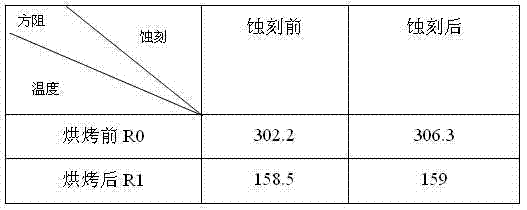
(2) sheet resistance is measured:
Adopt the impedance of Mitsubishi MCP-T360 working sample.
| ? | R0 before the baking | R1 after the baking |
| Sheet resistance (Ω/) | 302.2 | 158.5 |
(3) sticking power is measured
Adopt ZEHNTNER hundred lattice cuttves to mark the lattice 100 that is spaced apart 1 millimeter of uniform size at sample surfaces, firmly stick on specific adhesive tape and draw on the lattice surface, firmly tear, the lattice number that the statistics film comes off.
| ? | R0 before the baking | R1 after the baking |
| After tearing/before tearing (%) | 〉98% | 〉99% |
(4) bending is measured
Adopt HYCHTECH Testing Machine Corporation bending fatigue trier to measure the sample bending is Φ 10mm, the variation of sheet resistance after 20 times
(1) acidproof mensuration
Take out after sample placed standard etching solution solution 20min fully, measure etching before and after the sample sheet resistance have unchanged.
Claims (10)
1. ITO film that is used for touch-screen, this film comprises transparent base (1) and is plated on rete on the described transparent base, it is characterized in that: described rete comprises bottom (2), middle layer (3) and the first surface layer (4) that self-induced transparency matrix (1) upper surface is upwards arranged successively.
2. the ITO film for touch-screen according to claim 1, it is characterized in that: described bottom (2), middle layer (3) and the first surface layer (4) are single layer structure.
3. the ITO film for touch-screen according to claim 1, it is characterized in that: the thickness of described transparent base (1) is 50-188 μ m, described transparent base (1) is polyethylene terephthalate or poly-imines.
4. the ITO film for touch-screen according to claim 1, it is characterized in that: described bottom (2) is SiO
2Or Al
2O
3Described middle layer (3) is Si
3N
4Or Nb
2O
5Described the first surface layer (4) is the ITO layer.
5. preparation method such as the described ITO film for touch-screen of claim 1 to 4, it is characterized in that: the method is included under the magnetron sputtering condition, applying power supply at magnetic controlling target makes the target material sputter on the magnetic control target and deposits on the transparent base (1), to form rete at matrix, described rete comprises bottom (2), middle layer (3) and the first surface layer (4) that self-induced transparency matrix (1) upper surface is upwards arranged successively; Forming as mentioned above, rete all carries out under argon gas, nitrogen and/or oxygen atmosphere.
6. the preparation method of the ITO film for touch-screen according to claim 4, it is characterized in that: wherein, under the magnetron sputtering condition, described formation bottom (2) thickness is 12-60nm, described formation middle layer (3) thickness is 7-10nm, and described formation the first surface layer (4) thickness is 18-29nm.
7. the preparation method of the ITO film for touch-screen according to claim 4, it is characterized in that: described magnetic control target is tin indium oxide target material, composition is the Indium sesquioxide of 95wt% and the stannic oxide of 5wt%.
8. the preparation method of the ITO film for touch-screen according to claim 4, it is characterized in that: the sputtering condition of described formation bottom (2) film comprises that the power of power supply is 12-30kw, the vacuum tightness of magnetron sputtering is 9.0E-04--1.6E-03mbar, the flow of working gas is 260-320sccm, and sputter rate is 0.8-1.4m/min.
9. the preparation method of the ITO film for touch-screen according to claim 4, it is characterized in that: the sputtering condition of described formation middle layer (3) film comprises the power 6-8kw of power supply, the vacuum tightness of magnetron sputtering is 1.2E-03-1.4E-03mbar, the flow of working gas is 90-170sccm, and sputter rate is 0.8-1.4m/min.
10. the preparation method of the ITO film for touch-screen according to claim 4, it is characterized in that: the sputtering condition of described formation the first surface layer (4) film comprises that the power of power supply is 4.3-7kw, the vacuum tightness of magnetron sputtering is 2.0E-03-2.9E-03mbar, the flow of working gas is 255-325sccm, and sputter rate is 0.8-1.4m/min.
Priority Applications (1)
| Application Number | Priority Date | Filing Date | Title |
|---|---|---|---|
| CN2012105650971A CN103014644A (en) | 2012-12-24 | 2012-12-24 | ITO (indium tin oxide) film for touch screen and preparation method thereof |
Applications Claiming Priority (1)
| Application Number | Priority Date | Filing Date | Title |
|---|---|---|---|
| CN2012105650971A CN103014644A (en) | 2012-12-24 | 2012-12-24 | ITO (indium tin oxide) film for touch screen and preparation method thereof |
Publications (1)
| Publication Number | Publication Date |
|---|---|
| CN103014644A true CN103014644A (en) | 2013-04-03 |
Family
ID=47963752
Family Applications (1)
| Application Number | Title | Priority Date | Filing Date |
|---|---|---|---|
| CN2012105650971A Pending CN103014644A (en) | 2012-12-24 | 2012-12-24 | ITO (indium tin oxide) film for touch screen and preparation method thereof |
Country Status (1)
| Country | Link |
|---|---|
| CN (1) | CN103014644A (en) |
Cited By (7)
| Publication number | Priority date | Publication date | Assignee | Title |
|---|---|---|---|---|
| CN104651791A (en) * | 2015-02-18 | 2015-05-27 | 南京汇金锦元光电材料有限公司 | Energy-saving flexible transparent conducting film and preparation method thereof |
| CN104978075A (en) * | 2015-08-01 | 2015-10-14 | 安徽省蚌埠华益导电膜玻璃有限公司 | Touch screen and preparation method thereof |
| CN111560586A (en) * | 2020-04-30 | 2020-08-21 | 豪威星科薄膜视窗(深圳)有限公司 | Capacitive touch screen coating process and touch screen |
| CN112965148A (en) * | 2021-04-15 | 2021-06-15 | 信阳舜宇光学有限公司 | Optical material with ITO film layer and manufacturing method thereof |
| US11177447B2 (en) | 2017-08-17 | 2021-11-16 | Asustek Computer Inc. | Flexible display and manufacturing method thereof |
| CN117352582A (en) * | 2023-09-22 | 2024-01-05 | 福建金石能源有限公司 | A method for film formation of heterojunction cells |
| CN117865505A (en) * | 2023-12-28 | 2024-04-12 | 天津南玻节能玻璃有限公司 | Preparation method of ITO conductive glass and ITO conductive glass |
Citations (2)
| Publication number | Priority date | Publication date | Assignee | Title |
|---|---|---|---|---|
| DE102005015631A1 (en) * | 2005-04-05 | 2006-10-12 | Von Ardenne Anlagentechnik Gmbh | Large surface application of dielectric reflection decreasing scratch resistant layer system useful for synthetic plastic camera lenses and CD players and autoradio displays involves removal (sic) of layers |
| CN102324271A (en) * | 2011-10-14 | 2012-01-18 | 南昌欧菲光科技有限公司 | Crystallized type ITO (Indium Tin Oxide) transparent conductive film and preparation method thereof |
-
2012
- 2012-12-24 CN CN2012105650971A patent/CN103014644A/en active Pending
Patent Citations (2)
| Publication number | Priority date | Publication date | Assignee | Title |
|---|---|---|---|---|
| DE102005015631A1 (en) * | 2005-04-05 | 2006-10-12 | Von Ardenne Anlagentechnik Gmbh | Large surface application of dielectric reflection decreasing scratch resistant layer system useful for synthetic plastic camera lenses and CD players and autoradio displays involves removal (sic) of layers |
| CN102324271A (en) * | 2011-10-14 | 2012-01-18 | 南昌欧菲光科技有限公司 | Crystallized type ITO (Indium Tin Oxide) transparent conductive film and preparation method thereof |
Cited By (7)
| Publication number | Priority date | Publication date | Assignee | Title |
|---|---|---|---|---|
| CN104651791A (en) * | 2015-02-18 | 2015-05-27 | 南京汇金锦元光电材料有限公司 | Energy-saving flexible transparent conducting film and preparation method thereof |
| CN104978075A (en) * | 2015-08-01 | 2015-10-14 | 安徽省蚌埠华益导电膜玻璃有限公司 | Touch screen and preparation method thereof |
| US11177447B2 (en) | 2017-08-17 | 2021-11-16 | Asustek Computer Inc. | Flexible display and manufacturing method thereof |
| CN111560586A (en) * | 2020-04-30 | 2020-08-21 | 豪威星科薄膜视窗(深圳)有限公司 | Capacitive touch screen coating process and touch screen |
| CN112965148A (en) * | 2021-04-15 | 2021-06-15 | 信阳舜宇光学有限公司 | Optical material with ITO film layer and manufacturing method thereof |
| CN117352582A (en) * | 2023-09-22 | 2024-01-05 | 福建金石能源有限公司 | A method for film formation of heterojunction cells |
| CN117865505A (en) * | 2023-12-28 | 2024-04-12 | 天津南玻节能玻璃有限公司 | Preparation method of ITO conductive glass and ITO conductive glass |
Similar Documents
| Publication | Publication Date | Title |
|---|---|---|
| CN104651791B (en) | Energy-saving flexible transparent conductive film and preparation method thereof | |
| CN103014644A (en) | ITO (indium tin oxide) film for touch screen and preparation method thereof | |
| CN105951053B (en) | A kind of preparation method of titania-doped transparent conductive film of niobium and the titania-doped transparent conductive film of niobium | |
| CN204490985U (en) | Flexible transparent conductive film and preparation facilities thereof | |
| CN105821378B (en) | A kind of niobium-doped tin dioxide transparent conductive film and preparation method thereof | |
| CN101465172A (en) | Composite structure transparent conductive film and preparation method thereof | |
| CN106086789B (en) | Interfacial Layer Method for Deposition of Transparent Conductive Thin Films on Polyester Surfaces by Magnetron Sputtering | |
| CN101294272A (en) | Method for room temperature sputtering deposition of indium tin oxide transparent conductive film on flexible substrate | |
| CN102174689A (en) | FZO/metal/FZO transparent conductive film and preparation method thereof | |
| CN107245701A (en) | A kind of many target material magnetic sputtering winding film coating machines and film plating process | |
| TW201422836A (en) | Method for producing substrate with transparent electrode, and substrate with transparent electrode | |
| CN103436844A (en) | Coating device and method for depositing flexible substrate ITO film at low temperature | |
| CN107731352B (en) | Flexible electronic glass transparent conductive oxide film circuit preparation method | |
| CN101555589A (en) | Continuous winding magnetron sputtering double-surface ceramics high barrier film device | |
| CN102945694B (en) | ITO (indium tin oxide) base plate and preparation method of ITO base plate | |
| CN103924191A (en) | Method for plating ITO thin film on substrate | |
| CN202954086U (en) | Film plating device and target materials | |
| CN203487223U (en) | Coating device for depositing flexible base material ITO (Indium Tin Oxides) film at low temperature | |
| CN103489505B (en) | A kind of touch-screen ITO conducting film and preparation method thereof | |
| CN114231903B (en) | Niobium oxide/silver nanowire double-layer structure flexible transparent conductive film and preparation method thereof | |
| CN103000637A (en) | Coated thin film transistor (TFT) substrate, preparation method thereof and TFT | |
| CN206872938U (en) | Fexible film gap winds magnetic control sputtering vacuum coating machine | |
| CN207468716U (en) | A kind of double-face vacuum plated film up- coiler | |
| CN101748371B (en) | Method for preparing insulating film attached to touch screen | |
| CN104213090A (en) | A method for preparing molybdenum-doped zinc oxide thin film by magnetron sputtering |
Legal Events
| Date | Code | Title | Description |
|---|---|---|---|
| C06 | Publication | ||
| PB01 | Publication | ||
| C10 | Entry into substantive examination | ||
| SE01 | Entry into force of request for substantive examination | ||
| C02 | Deemed withdrawal of patent application after publication (patent law 2001) | ||
| WD01 | Invention patent application deemed withdrawn after publication |
Application publication date: 20130403 |