[go: up one dir, main page]

CN102812519A - Composite semiconductor memory device with error correction - Google Patents

Composite semiconductor memory device with error correction Download PDF

Info

Publication number
CN102812519A
CN102812519A CN201180014974XA CN201180014974A CN102812519A CN 102812519 A CN102812519 A CN 102812519A CN 201180014974X A CN201180014974X A CN 201180014974XA CN 201180014974 A CN201180014974 A CN 201180014974A CN 102812519 A CN102812519 A CN 102812519A
Authority
CN
China
Prior art keywords
compound semiconductor
semiconductor memory
memory device
interface
data
Prior art date
Legal status (The legal status is an assumption and is not a legal conclusion. Google has not performed a legal analysis and makes no representation as to the accuracy of the status listed.)
Pending
Application number
CN201180014974XA
Other languages
Chinese (zh)
Inventor
金镇祺
Current Assignee (The listed assignees may be inaccurate. Google has not performed a legal analysis and makes no representation or warranty as to the accuracy of the list.)
Mosaid Technologies Inc
Original Assignee
Mosaid Technologies Inc
Priority date (The priority date is an assumption and is not a legal conclusion. Google has not performed a legal analysis and makes no representation as to the accuracy of the date listed.)
Filing date
Publication date
Application filed by Mosaid Technologies Inc filed Critical Mosaid Technologies Inc
Publication of CN102812519A publication Critical patent/CN102812519A/en
Pending legal-status Critical Current

Links

Images

Classifications

    • GPHYSICS
    • G06COMPUTING OR CALCULATING; COUNTING
    • G06FELECTRIC DIGITAL DATA PROCESSING
    • G06F11/00Error detection; Error correction; Monitoring
    • G06F11/07Responding to the occurrence of a fault, e.g. fault tolerance
    • G06F11/08Error detection or correction by redundancy in data representation, e.g. by using checking codes
    • G06F11/10Adding special bits or symbols to the coded information, e.g. parity check, casting out 9's or 11's
    • G06F11/1008Adding special bits or symbols to the coded information, e.g. parity check, casting out 9's or 11's in individual solid state devices
    • G06F11/1044Adding special bits or symbols to the coded information, e.g. parity check, casting out 9's or 11's in individual solid state devices with specific ECC/EDC distribution
    • GPHYSICS
    • G11INFORMATION STORAGE
    • G11CSTATIC STORES
    • G11C29/00Checking stores for correct operation ; Subsequent repair; Testing stores during standby or offline operation
    • G11C29/04Detection or location of defective memory elements, e.g. cell constructio details, timing of test signals
    • G11C29/08Functional testing, e.g. testing during refresh, power-on self testing [POST] or distributed testing
    • G11C29/12Built-in arrangements for testing, e.g. built-in self testing [BIST] or interconnection details
    • G11C29/38Response verification devices
    • G11C29/42Response verification devices using error correcting codes [ECC] or parity check
    • GPHYSICS
    • G06COMPUTING OR CALCULATING; COUNTING
    • G06FELECTRIC DIGITAL DATA PROCESSING
    • G06F11/00Error detection; Error correction; Monitoring
    • G06F11/07Responding to the occurrence of a fault, e.g. fault tolerance
    • G06F11/08Error detection or correction by redundancy in data representation, e.g. by using checking codes
    • G06F11/10Adding special bits or symbols to the coded information, e.g. parity check, casting out 9's or 11's
    • G06F11/1008Adding special bits or symbols to the coded information, e.g. parity check, casting out 9's or 11's in individual solid state devices
    • G06F11/1048Adding special bits or symbols to the coded information, e.g. parity check, casting out 9's or 11's in individual solid state devices using arrangements adapted for a specific error detection or correction feature
    • HELECTRICITY
    • H03ELECTRONIC CIRCUITRY
    • H03MCODING; DECODING; CODE CONVERSION IN GENERAL
    • H03M13/00Coding, decoding or code conversion, for error detection or error correction; Coding theory basic assumptions; Coding bounds; Error probability evaluation methods; Channel models; Simulation or testing of codes
    • H03M13/03Error detection or forward error correction by redundancy in data representation, i.e. code words containing more digits than the source words
    • H03M13/05Error detection or forward error correction by redundancy in data representation, i.e. code words containing more digits than the source words using block codes, i.e. a predetermined number of check bits joined to a predetermined number of information bits
    • HELECTRICITY
    • H03ELECTRONIC CIRCUITRY
    • H03MCODING; DECODING; CODE CONVERSION IN GENERAL
    • H03M13/00Coding, decoding or code conversion, for error detection or error correction; Coding theory basic assumptions; Coding bounds; Error probability evaluation methods; Channel models; Simulation or testing of codes
    • H03M13/61Aspects and characteristics of methods and arrangements for error correction or error detection, not provided for otherwise
    • H03M13/611Specific encoding aspects, e.g. encoding by means of decoding
    • GPHYSICS
    • G11INFORMATION STORAGE
    • G11CSTATIC STORES
    • G11C29/00Checking stores for correct operation ; Subsequent repair; Testing stores during standby or offline operation
    • G11C29/04Detection or location of defective memory elements, e.g. cell constructio details, timing of test signals
    • G11C2029/0411Online error correction

Landscapes

  • Engineering & Computer Science (AREA)
  • Theoretical Computer Science (AREA)
  • Physics & Mathematics (AREA)
  • Quality & Reliability (AREA)
  • General Engineering & Computer Science (AREA)
  • General Physics & Mathematics (AREA)
  • Probability & Statistics with Applications (AREA)
  • Techniques For Improving Reliability Of Storages (AREA)
  • Read Only Memory (AREA)
  • For Increasing The Reliability Of Semiconductor Memories (AREA)

Abstract

A composite semiconductor memory device, comprising: a plurality of nonvolatile memory devices; and an interface device connected to the plurality of nonvolatile memory devices and for connection to a memory controller, the interface device comprising an error correction coding (ECC) engine. Also, a memory system, comprising: a memory controller; and at least one composite semiconductor memory device configured for being written to and read from by the memory controller and comprising a built-in error correction coding (ECC) engine. Also, a memory system, comprising: a composite semiconductor memory device comprising a plurality of nonvolatile memory devices; and a memory controller connected to the at least one composite semiconductor memory device, for issuing read and write commands to the composite semiconductor memory device to cause data to be written to or read from individual ones of the nonvolatile memory devices; the composite semiconductor memory device providing error-free writing and reading of the data.

Description

具有错误校正的复合半导体存储设备Compound semiconductor memory device with error correction

背景技术 Background technique

诸如数字音频/视频播放器、蜂窝电话、便携式通用串行总线(USB)驱动和固态驱动(SSD)之类的消费者电子设备的数据存储需要已经明显增长了。结合了闪存(一般称为闪存设备)的非易失性半导体存储设备能够以相对低的成本来满足该密度需求。目前,有两种主要类型的闪存,即NOR闪存和NAND闪存,而且在这两种闪存中,NAND闪存已经被证明尤其受欢迎。The data storage needs of consumer electronic devices such as digital audio/video players, cellular phones, portable Universal Serial Bus (USB) drives and solid-state drives (SSDs) have increased significantly. Non-volatile semiconductor memory devices incorporating flash memory (commonly referred to as flash memory devices) can meet this density requirement at relatively low cost. Currently, there are two main types of flash memory, NOR flash memory and NAND flash memory, and of the two, NAND flash memory has proven particularly popular.

然而,随着闪存设备变得更密集和更便宜,期望它们提供的存储量进一步增加。该期望继而施加了进一步的压力以便以甚至更低的成本来使得这些设备更为密集。However, as flash memory devices become denser and cheaper, the amount of storage they provide is expected to increase further. This expectation in turn exerts further pressure to make these devices more dense at even lower cost.

发明内容 Contents of the invention

根据本发明的一个方面,提供一种复合半导体存储设备,包括:多个非易失性存储设备;以及接口设备,其连接到所述多个非易失性存储设备并用于连接到存储控制器,该接口设备包括纠错编码(ECC)引擎。According to an aspect of the present invention, there is provided a composite semiconductor storage device including: a plurality of nonvolatile storage devices; and an interface device connected to the plurality of nonvolatile storage devices for connection to a storage controller , the interface device includes an error correction coding (ECC) engine.

根据本发明的另一方面,提供一种存储系统,包括:存储控制器;以及至少一个复合半导体存储设备,其被配置为由所述存储控制器写入和读取并包括内置的纠错编码(ECC)引擎。According to another aspect of the present invention, there is provided a memory system comprising: a memory controller; and at least one compound semiconductor memory device configured to be written to and read by the memory controller and including a built-in error correction code (ECC) engine.

根据本发明的另一方面,提供一种存储系统,包括:复合半导体存储设备,其包括多个非易失性存储设备;以及存储控制器,其连接到至少一个复合半导体存储设备,用于向所述复合半导体存储设备发布读取和写入命令以促使数据被写入所述非易失性存储设备中的特定一些非易失性存储设备或者被从所述非易失性存储设备中的特定一些非易失性存储设备中读取;从存储控制器的角度,该复合半导体存储设备提供数据的无错误写入和读取。According to another aspect of the present invention, there is provided a storage system comprising: a composite semiconductor storage device including a plurality of nonvolatile storage devices; and a storage controller connected to at least one composite semiconductor storage device for providing The compound semiconductor memory device issues read and write commands to cause data to be written into specific ones of the nonvolatile memory devices or to be read from Read from certain non-volatile memory devices; from the perspective of the memory controller, the compound semiconductor memory device provides error-free writing and reading of data.

在阅读了下面结合附图对本发明具体实施方式的描述之后,本发明的其他方面和特征对本领域普通技术人员而言将变得显而易见。Other aspects and features of the present invention will become apparent to those of ordinary skill in the art after reading the following description of specific embodiments of the present invention in conjunction with the accompanying drawings.

附图说明 Description of drawings

现在将参照附图、仅通过示例的方式描述本发明的实施方式,其中:Embodiments of the invention will now be described, by way of example only, with reference to the accompanying drawings, in which:

图1是示出了根据非限制性实施方式的非易失性存储系统的框图;Figure 1 is a block diagram illustrating a non-volatile storage system according to a non-limiting embodiment;

图2是示出了根据非限制性实施方式的使用单个复合半导体存储设备的非易失性存储系统的框图;2 is a block diagram illustrating a non-volatile memory system using a single composite semiconductor memory device according to a non-limiting embodiment;

图3-5是示出了根据非限制性实施方式的使用多个复合半导体存储设备的非易失性存储系统的框图;3-5 are block diagrams illustrating non-volatile memory systems using multiple composite semiconductor memory devices according to non-limiting embodiments;

图6是示出了根据非限制性实施方式的复合半导体存储设备的某些部件的框图;6 is a block diagram illustrating certain components of a compound semiconductor memory device according to a non-limiting embodiment;

图7A、7B、8A和8B描绘了根据非限制性实施方式的复合半导体存储设备的截面视图;7A, 7B, 8A and 8B depict cross-sectional views of compound semiconductor memory devices according to non-limiting embodiments;

图9是示出了NAND闪存功能块的框图;Fig. 9 is a block diagram showing NAND flash memory functional blocks;

图10是示出了NAND闪存单元阵列结构的框图;Figure 10 is a block diagram showing the structure of a NAND flash memory cell array;

图11是示出了NAND闪存块结构的框图;Fig. 11 is a block diagram showing the block structure of NAND flash memory;

图12是示出了NAND闪存页结构的框图;Figure 12 is a block diagram showing the NAND flash page structure;

图13是示出了NAND闪存中的基于页的读取操作的框图;13 is a block diagram illustrating a page-based read operation in NAND flash memory;

图14是示出了NAND闪存中的基于页的编程操作的框图;14 is a block diagram illustrating a page-based programming operation in NAND flash memory;

图15是示出了NAND闪存中的基于块的擦除操作的框图;FIG. 15 is a block diagram illustrating block-based erase operations in NAND flash memory;

图16是示出了根据非限制性实施方式的复合半导体存储设备的内部功能架构的框图,其中多个非易失性半导体存储设备以多分支(multi-drop)的方式互连;16 is a block diagram illustrating an internal functional architecture of a compound semiconductor memory device in which a plurality of nonvolatile semiconductor memory devices are interconnected in a multi-drop manner according to a non-limiting embodiment;

图17是示出了图16中的到多个非易失性半导体存储设备的多分支互连的更多细节的框图;FIG. 17 is a block diagram showing more details of the multi-drop interconnection to a plurality of non-volatile semiconductor memory devices in FIG. 16;

图18是示出了根据非限制性实施方式的复合半导体存储设备的内部功能架构的框图,其中多个非易失性存储设备使用专用接口通道进行互连;18 is a block diagram illustrating the internal functional architecture of a composite semiconductor memory device in which multiple non-volatile memory devices are interconnected using dedicated interface channels, according to a non-limiting embodiment;

图19是示出了根据非限制性实施方式的复合半导体存储设备的内部功能架构的框图,其中多个非易失性存储设备使用基于组的接口通道进行互连;19 is a block diagram illustrating the internal functional architecture of a compound semiconductor memory device in which multiple non-volatile memory devices are interconnected using group-based interface channels, according to a non-limiting embodiment;

图20、21和22是示出了根据非限制性实施方式的复合半导体存储设备的不同内部配置的框图;20, 21 and 22 are block diagrams showing different internal configurations of a compound semiconductor memory device according to a non-limiting embodiment;

图23是示出了纠错编码过程的框图;Figure 23 is a block diagram illustrating an error correction encoding process;

图24是示出了纠错解码过程的框图;FIG. 24 is a block diagram illustrating an error correction decoding process;

图25-26突出显示了根据非限制性实施方式的被写入接口设备的数据与由接口设备写入非易失性存储设备的数据之间的差异;以及25-26 highlight differences between data written to an interface device and data written by an interface device to a non-volatile storage device, according to non-limiting embodiments; and

图27是根据非限制性实施方式的存储控制器的功能框图。Figure 27 is a functional block diagram of a memory controller according to a non-limiting embodiment.

具体实施方式 Detailed ways

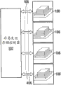
图1示出了根据非限制性实施方式的非易失性存储系统100的框图。非易失性存储系统100包括存储控制器102,该存储控制器102用于经由通信链路104与主系统或处理器98通信。非易失性存储系统100还包括经由通信链路108连接到存储控制器102的至少一个复合半导体存储设备106。存储控制器102可以是闪存控制器。FIG. 1 shows a block diagram of a non-volatile storage system 100 according to a non-limiting embodiment. Non-volatile storage system 100 includes a storage controller 102 for communicating with a host system or processor 98 via a communication link 104 . Non-volatile memory system 100 also includes at least one compound semiconductor memory device 106 connected to memory controller 102 via communication link 108 . Storage controller 102 may be a flash memory controller.

在非限制性实施方式中,如图2所示,在非易失性存储系统100中可以存在单个复合半导体存储设备106。在其他非限制性实施方式中,如图3、4和5所示,在非易失性存储系统100中可以存在多个半导体存储设备106。虽然示出了四个(4)半导体存储设备106,但是应当理解,对能够被包括在非易失性存储系统100中的复合半导体设备106的数量没有特别的限制。In a non-limiting implementation, as shown in FIG. 2 , there may be a single composite semiconductor memory device 106 in the non-volatile memory system 100 . In other non-limiting implementations, as shown in FIGS. 3 , 4 and 5 , there may be multiple semiconductor storage devices 106 in the non-volatile storage system 100 . Although four (4) semiconductor memory devices 106 are shown, it should be understood that there is no particular limit to the number of compound semiconductor devices 106 that can be included in the nonvolatile memory system 100 .

在在非易失性存储系统100中有多个复合半导体设备106的实施方式中,通信链路108可以采取各种形式。特别地,根据图3中所示的非限制性实施方式,通信链路108可以包括公共接口通道(例如,多分支并行总线)302。另外,专用芯片使能信号304能够被提供给各个复合半导体存储设备106。能够通过断言(assert)相应的专用芯片使能信号304来选择单独的复合半导体存储设备106。根据图4中所示的非限制性实施方式,通信链路108能够在存储控制器102与复合半导体存储设备106之间应用多个专用接口通道406。在这种情况中,每个复合半导体存储设备106具有其自己的专用接口通道406。根据图5中所示的非限制性实施方式,通信链路108能够在存储控制器102与复合半导体存储设备106之间应用多个专用接口通道506。在这种情况中,每个公共接口通道506由一组两个(2)或更多个复合半导体存储设备106所共享。In implementations in which there are multiple compound semiconductor devices 106 in the non-volatile storage system 100, the communication link 108 may take various forms. In particular, according to the non-limiting implementation shown in FIG. 3 , the communication link 108 may include a common interface channel (eg, a multi-drop parallel bus) 302 . In addition, a dedicated chip enable signal 304 can be provided to each compound semiconductor memory device 106 . Individual compound semiconductor memory devices 106 can be selected by asserting corresponding dedicated chip enable signals 304 . According to a non-limiting embodiment shown in FIG. 4 , communication link 108 is capable of employing a plurality of dedicated interface channels 406 between memory controller 102 and compound semiconductor memory device 106 . In this case, each compound semiconductor memory device 106 has its own dedicated interface channel 406 . According to a non-limiting embodiment shown in FIG. 5 , the communication link 108 is capable of employing a plurality of dedicated interface channels 506 between the memory controller 102 and the compound semiconductor memory device 106 . In this case, each common interface channel 506 is shared by a group of two (2) or more compound semiconductor memory devices 106 .

在非限制性实施方式中并参照图6,复合半导体存储设备106包括多个非易失性存储设备602A、602B、602C、602D和接口设备604。虽然示出了四个(4)非易失性存储设备602A、602B、602C、602D,但是应当理解,对可以连接到接口设备604的非易失性存储设备602A、602B、602C、602D的数量没有特别限制。通过使用接口通道来实现接口设备604与非易失性存储设备602A、602B、602C、602D之间的通信,这将在后面参照图16-19来描述。接口设备604能够包括纠错编码(ECC)引擎606。ECC引擎606允许复合存储设备106呈现向非易失性存储设备602A、602B、602C、602D的无错误数据写入(如从存储控制器102的角度所判断的)以及从非易失性存储设备602A、602B、602C、602D的无错误数据读取(如从存储控制器102的角度所判断的)。In a non-limiting embodiment and referring to FIG. 6 , the composite semiconductor memory device 106 includes a plurality of non-volatile memory devices 602A, 602B, 602C, 602D and an interface device 604 . Although four (4) non-volatile storage devices 602A, 602B, 602C, 602D are shown, it should be understood that the number of non-volatile storage devices 602A, 602B, 602C, 602D that can be connected to the interface device There are no particular restrictions. The communication between the interface device 604 and the non-volatile storage devices 602A, 602B, 602C, 602D is realized by using an interface channel, which will be described later with reference to FIGS. 16-19 . Interface device 604 can include an error correction coding (ECC) engine 606 . ECC engine 606 allows composite storage device 106 to exhibit error-free data writes to nonvolatile storage devices 602A, 602B, 602C, 602D (as judged from the perspective of storage controller 102) Error-free data reads of 602A, 602B, 602C, 602D (as judged from the perspective of the storage controller 102).

参照图7A、7B、8A和8B,接口设备604和非易失性存储设备602A、602B、602C、602D能够被封装在单个壳体704中,诸如多芯片封装(MCP)。具体地,非易失性存储设备602A、602B、602C、602D一起堆叠到基底706上。在图7A和8A中,接口设备604被示为放置在非易失性存储设备602D的顶部,而在图7B和8B中,接口设备604被示为位于非易失性存储设备的堆叠的底部。在不背离本发明的范围的情况下,其他配置也是可能的。还示出了附设到基底706上以允许复合半导体存储设备106与其外部的其他部件之间的电连接的焊盘708。也提供在接口设备604与非易失性存储设备602A、602B、602C、602D中的每个非易失性存储设备之间的连接。而且,在图7A和7B的实施方式中,通过基底706在接口设备604与非易失性存储设备602A、602B、602C、602D中的每个非易失性存储设备之间建立引线键合702。相反地,在图8A和8B的实施方式中,在接口设备604与非易失性存储设备602A、602B、602C、602D中的每个非易失性存储设备之间建立直接连接802。将接口设备604与非易失性存储设备602A、602B、602C、602D中的每个非易失性存储设备互连的其他方式也是可能的。而且,虽然示出了堆叠的管芯(die)配置,但是这不应被解释为是限制性的。Referring to Figures 7A, 7B, 8A and 8B, the interface device 604 and the non-volatile storage devices 602A, 602B, 602C, 602D can be packaged in a single housing 704, such as a multi-chip package (MCP). Specifically, the non-volatile storage devices 602A, 602B, 602C, 602D are stacked together onto the substrate 706 . In FIGS. 7A and 8A, the interface device 604 is shown placed on top of the non-volatile storage device 602D, while in FIGS. 7B and 8B, the interface device 604 is shown at the bottom of the stack of non-volatile storage devices. . Other configurations are also possible without departing from the scope of the present invention. Also shown are pads 708 attached to the substrate 706 to allow electrical connection between the composite semiconductor memory device 106 and other components external thereto. Connections between the interface device 604 and each of the non-volatile storage devices 602A, 602B, 602C, 602D are also provided. Moreover, in the embodiment of FIGS. 7A and 7B , wire bonds 702 are established between the interface device 604 and each of the non-volatile storage devices 602A, 602B, 602C, 602D through the substrate 706. . In contrast, in the embodiment of Figures 8A and 8B, a direct connection 802 is established between the interface device 604 and each of the non-volatile storage devices 602A, 602B, 602C, 602D. Other ways of interconnecting the interface device 604 with each of the non-volatile storage devices 602A, 602B, 602C, 602D are also possible. Also, while a stacked die configuration is shown, this should not be construed as limiting.

非易失性存储设备602A、602B、602C、602DNon-volatile storage devices 602A, 602B, 602C, 602D

非易失性存储设备602A、602B、602C、602D可以是NAND闪存设备、NOR闪存设备或相变存储设备,这仅给出了几个非限制性的可能性。非易失性存储设备602A、602B、602C、602D能够异步或同步地操作,这仅给出了几个非限制性的可能性。而且,非易失性存储设备602A、602B、602C、602D能够作为单数据速率(SDR)设备或双数据速率(DDR)设备进行操作,这仅给出了几个非限制性的可能性。在特定的非限制性实施方式中,非易失性存储设备602A、602B、602C、602D能够遵守工业规范,诸如三星的针对产品K9GAG08U0D、K9LBG08U1D、K9HCG08U5D的16Gb多级别单元NAND闪存规范(其在能够从三星电子获得的名称为“2Gx8Bit/4Gx8Bit/8Gx8BitNAND Flash Memory”的文档中描述),其提供了设备操作和时序细节且通过引用而被合并到本文。当然,可获得的闪存的其他制备或模型能够用作非易失性存储设备602A、602B、602C、602D。The non-volatile memory devices 602A, 602B, 602C, 602D may be NAND flash devices, NOR flash devices or phase change memory devices, just to give a few non-limiting possibilities. The non-volatile storage devices 602A, 602B, 602C, 602D can operate asynchronously or synchronously, just to give a few non-limiting possibilities. Also, the non-volatile memory devices 602A, 602B, 602C, 602D can operate as single data rate (SDR) devices or double data rate (DDR) devices, just to give a few non-limiting possibilities. In a particular non-limiting embodiment, the non-volatile memory devices 602A, 602B, 602C, 602D are capable of complying with industry specifications, such as Samsung's 16Gb multi-level cell NAND flash memory specification for products K9GAG08U0D, K9LBG08U1D, K9HCG08U5D (which can be Described in a document titled "2Gx8Bit/4Gx8Bit/8Gx8BitNAND Flash Memory" obtained from Samsung Electronics), which provides device operation and timing details and is incorporated herein by reference. Of course, other preparations or models of flash memory available can be used as non-volatile storage devices 602A, 602B, 602C, 602D.

图9概念性地示出了被实现为NAND闪存设备的非易失性存储设备(诸如,在该示例中,设备602A)的各种功能部件。Figure 9 conceptually illustrates various functional components of a non-volatile storage device, such as, in this example, device 602A, implemented as a NAND flash memory device.

设备602A使用下面的端口和信号:Device 602A uses the following ports and signals:

·输入/输出(I/O)端口(I/O0至I/O7):I/O端口被用于传输去向和来自设备602A的地址、命令和输入/输出数据。特别地,要被写入设备602A的数据到达I/O端口I/O0至I/O7并在被存储到存储单元阵列902之前被临时放置在一组全局缓冲器916中。要从设备602A中读取的数据被从存储单元阵列902中提取,并在在I/O端口I/O0至I/O7上被释放之前被放置在这组全局缓冲器916中。• Input/Output (I/O) Ports (I/O0 to I/O7): I/O ports are used to transmit addresses, commands, and input/output data to and from device 602A. In particular, data to be written to device 602A arrives at I/O ports I/O0 through I/O7 and is temporarily placed in a set of global buffers 916 before being stored in memory cell array 902 . Data to be read from device 602A is fetched from memory cell array 902 and placed in set of global buffers 916 before being freed on I/O ports I/O0 through I/O7.

·写使能端口(WE#):该WE#端口接收WE#信号,该WE#信号用于控制从I/O端口的数据的获取;Write enable port (WE#): The WE# port receives the WE# signal, which is used to control the acquisition of data from the I/O port;

·命令锁存使能(CLE)端口:该CLE端口接收CLE信号,该CLE信号用于控制操作模式命令向命令寄存器910的加载。在CLE信号被断言时,该命令在WE#信号的上升沿被从I/O端口锁存到命令寄存器910中;• Command Latch Enable (CLE) Port: The CLE port receives the CLE signal, which is used to control the loading of the operating mode commands to the command register 910 . When the CLE signal is asserted, the command is latched from the I/O port into the command register 910 on the rising edge of the WE# signal;

·地址锁存使能(ALE)端口:该ALE端口接收ALE信号,该ALE信号用于控制地址信息向内部地址寄存器912的加载。在ALE信号被断言时,该地址信息在WE#信号的上升沿被从I/O端口锁存到地址寄存器912中;• Address Latch Enable (ALE) port: The ALE port receives the ALE signal, which is used to control the loading of address information into the internal address register 912 . When the ALE signal is asserted, the address information is latched from the I/O port into the address register 912 at the rising edge of the WE# signal;

·准备就绪/忙(R/B#)端口:该R/B#端口是开漏引脚而且输出R/B#信号由设备602用来指示其操作状态。具体地,该R/B#信号指示该设备是准备就绪还是忙。设备602A中的R/B#电路914将在设备602A处于忙状态(诸如在读取、编程和擦除操作期间)中时解除断言(de-assert)该R/B#信号。在操作完成之后,该R/B#电路914将重新断言R/B#信号,从而指示设备602A处于准备就绪状态中。• Ready/Busy (R/B#) Port: The R/B# port is an open-drain pin and the output R/B# signal is used by the device 602 to indicate its operating status. Specifically, the R/B# signal indicates whether the device is ready or busy. R/B# circuitry 914 in device 602A will de-assert the R/B# signal when device 602A is in a busy state, such as during read, program, and erase operations. After the operation is complete, the R/B# circuit 914 will re-assert the R/B# signal, indicating that the device 602A is in a ready state.

·芯片使能(CE#)端口:该CE#端口接收CE#信号。当CE#信号在设备602A处于准备就绪状态中(当R/B#信号被断言时)被解除断言时,设备602A进入低功率待机模式。然而,当设备602A处于忙状态中时(当R/B#信号被解除断言时),诸如在读取、编程或擦除操作期间,该CE#信号被忽略。也就是说,如果设备602A处于忙状态,则设备602A不会进入待机模式,而不管CE#信号是否被解除断言。·Chip enable (CE#) port: The CE# port receives CE# signal. When the CE# signal is deasserted while the device 602A is in the ready state (when the R/B# signal is asserted), the device 602A enters a low power standby mode. However, the CE# signal is ignored when device 602A is in a busy state (when the R/B# signal is deasserted), such as during a read, program, or erase operation. That is, if device 602A is in a busy state, device 602A will not enter standby mode regardless of whether the CE# signal is deasserted.

·读使能(RE#)端口:该RE#端口接收用于控制串行数据输出的RE#信号。具体地,在RE#信号的下降沿之后(即当RE#信号被断言时),将由设备602A输出的数据放置在I/O端口I/O0至I/O7上。内部列地址计数器也在RE#信号的下降沿处被递增(地址=地址+1)。• Read Enable (RE#) Port: The RE# port receives the RE# signal used to control serial data output. Specifically, data output by device 602A is placed on I/O ports I/O0 through I/O7 after the falling edge of the RE# signal (ie, when the RE# signal is asserted). The internal column address counter is also incremented on the falling edge of the RE# signal (address = address + 1).

·写保护(WP#)端口:该WP#端口接收用于避免设备602A意外编程或擦除的WP#信号。内部电压调节器(高电压生成器918,其在读取、编程和擦除操作期间提供必要的高电压和参考电压)在WP#信号被断言时被复位。WP#信号能够用于在输入信号无效的加电/断电序列期间保护存储在存储单元阵列902中的数据。• Write Protect (WP#) Port: The WP# port receives the WP# signal used to prevent accidental programming or erasing of the device 602A. The internal voltage regulator (high voltage generator 918, which provides the necessary high voltage and reference voltage during read, program and erase operations) is reset when the WP# signal is asserted. The WP# signal can be used to protect data stored in the memory cell array 902 during a power up/down sequence where the input signal is inactive.

图10示出了存储单元阵列902的单元阵列结构,该单元阵列结构包括n个可擦除块1002-0至1002-(n-1)。每个块被再分成m个可编程页1102-0至1102-(m-1),如图11所示。继而,每个页被再分成(j+k)个8比特的字节,如图12所示。具体地,每页的字节被划分成j字节的数据存储区域(数据字段1202)和k字节的数据存储区域(备用字段1204)。因此,存储单元阵列902的总大小是n个块,这对应于(n*m)个页并因此等于(n*m*(j+k))个字节。FIG. 10 shows a cell array structure of a memory cell array 902 including n erasable blocks 1002 - 0 to 1002 -(n−1). Each block is subdivided into m programmable pages 1102 - 0 to 1102 -(m-1), as shown in FIG. 11 . Then, each page is subdivided into (j+k) 8-bit bytes, as shown in FIG. 12 . Specifically, the bytes of each page are divided into a data storage area of j bytes (data field 1202 ) and a data storage area of k bytes (spare field 1204 ). Thus, the total size of the memory cell array 902 is n blocks, which corresponds to (n*m) pages and thus equals (n*m*(j+k)) bytes.

备用字段1204能够用于错误管理功能(例如,存储错误控制编码奇偶校验位)。而且,依赖于实施方式,每一页和/或块的元数据(诸如擦除周期的数量、地址信息、坏块信息等)能够存储在数据字段1202中或备用字段1204中。Spare field 1204 can be used for error management functions (eg, storing error control coded parity bits). Also, metadata for each page and/or block (such as number of erase cycles, address information, bad block information, etc.) can be stored in the data field 1202 or in the spare field 1204, depending on the implementation.

NAND闪存中的备用字段1204的所需要的大小取决于页大小、工艺技术、每单元比特的数量(即每单元一个比特、每单元两个比特、每单元三个比特等等)和误码率。早期时代的NAND闪存中的页大小对于数据字段1202而言是512字节以及对于备用字段1204而言是16字节。随着工艺技术的演进,页大小已经增长了,这允许实现更大的存储密度。然而,该增长也带来了更高的误码率,因此需要使用更强的纠错编码。当前的页大小的示例对于数据字段1202而言是8K字节以及对于备用字段1204而言是436字节。而且,数据字段1202和备用字段1204的大小在闪存的制造商之间也会不同。然而,本领域技术人员应当意识到,本发明的实施方式并没有对数据字段1202的绝对或相对大小或对备用字段1204施加特定的限制。The required size of the spare field 1204 in NAND flash depends on the page size, process technology, number of bits per cell (i.e. one bit per cell, two bits per cell, three bits per cell, etc.) and bit error rate . The page size in early era NAND flash was 512 bytes for the data field 1202 and 16 bytes for the spare field 1204 . As process technology has evolved, page sizes have grown, allowing greater storage densities to be achieved. However, this increase also brings with it a higher bit error rate, requiring the use of stronger error correction codes. An example of a current page size is 8K bytes for the data field 1202 and 436 bytes for the spare field 1204 . Also, the size of the data field 1202 and the spare field 1204 may vary between manufacturers of flash memory. However, those skilled in the art should appreciate that the embodiments of the present invention impose no specific restrictions on the absolute or relative size of the data field 1202 or on the spare field 1204 .

再次参照图9,除了存储单元阵列902之外,设备602A的存储器核还包括行解码器920、读出放大器/页缓冲器904和列解码器922。行解码器920用于为读取操作或编程操作选择页,或者用于为擦除操作选择块。Referring again to FIG. 9 , in addition to memory cell array 902 , the memory core of device 602A includes row decoder 920 , sense amplifier/page buffer 904 and column decoder 922 . The row decoder 920 is used to select a page for a read operation or a program operation, or to select a block for an erase operation.

更具体地,在读取操作期间,存储单元阵列902中所选页上的数据被感测并锁存到读出放大器/页缓冲器904中。之后,通过列解码器922和全局缓冲器916顺序地读出存储在读出放大器/页缓冲器904中的数据。在编程操作期间,来自全局缓冲器916的输入数据经由列解码器922被顺序地加载到读出放大器/页缓冲器904中。被锁存到读出放大器/页缓冲器904中的输入数据之后被编程到存储单元阵列902的所选页中。More specifically, during a read operation, data on a selected page in memory cell array 902 is sensed and latched into sense amplifier/page buffer 904 . Thereafter, the data stored in the sense amplifier/page buffer 904 is sequentially read out through the column decoder 922 and the global buffer 916 . During a program operation, input data from global buffer 916 is sequentially loaded into sense amplifier/page buffer 904 via column decoder 922 . The input data latched into sense amplifier/page buffer 904 is then programmed into a selected page of memory cell array 902 .

设备602A还包括状态寄存器928,该状态寄存器在读取、编程或擦除操作期间跟踪设备602A的状态。该状态能够被编码以反映操作是已经通过还是失败以及设备602A是忙还是准备就绪。Device 602A also includes a status register 928 that tracks the status of device 602A during a read, program, or erase operation. The status can be coded to reflect whether the operation has passed or failed and whether the device 602A is busy or ready.

设备602A进一步包括控制电路930,该控制电路是具有状态机的中央单元,该状态机用于在各种操作模式期间控制设备602A。例如,前述的命令寄存器910解码来自全局缓冲器916的输入命令,并且解码后的命令被输入到控制电路930。The device 602A further includes a control circuit 930, which is a central unit having a state machine for controlling the device 602A during various modes of operation. For example, the aforementioned command register 910 decodes an input command from the global buffer 916 , and the decoded command is input to the control circuit 930 .

另外,设备602A包括控制缓冲器932,该控制缓冲器基于输入端口即CE#、CLE、ALE、WE#、RE#和WP#端口上的当前信号组合来确定当前的操作模式(诸如命令输入、地址输入、数据输入、数据输出和状态输出)。Additionally, device 602A includes a control buffer 932 that determines the current mode of operation based on the current combination of signals on the input ports, CE#, CLE, ALE, WE#, RE#, and WP# ports (such as command input, address input, data input, data output, and status output).

而且,设备602A包括前述的地址寄存器912,该地址寄存器存储多路复用后的列地址和行地址。该地址由地址寄存器解复用并被传输到行预解码器934和列预解码器936中。Furthermore, the device 602A includes the aforementioned address register 912, which stores the multiplexed column address and row address. The address is demultiplexed by the address register and passed into row predecoder 934 and column predecoder 936 .

在操作时,读取、编程和擦除操作由命令驱动。读取和编程操作以页为基础执行,而擦除操作以块为基础执行。对于本示例,假设j=4096(=4K)、k=218、m=128和n=4096。因此,页、块、平面(plane)和设备的容量如下给出:In operation, read, program and erase operations are command driven. Read and program operations are performed on a page basis, while erase operations are performed on a block basis. For this example, assume j=4096(=4K), k=218, m=128, and n=4096. Thus, the capacities of pages, blocks, planes, and devices are given by:

1页=(4K+218)字节;1 page = (4K+218) bytes;

1块=128页=(4K+218)字节x128=(512K+27.25K)字节;1 block = 128 pages = (4K+218) bytes x 128 = (512K+27.25K) bytes;

1平面=2048块=(512K+27.25K)字节x2048=(8G+436M)比特;1 plane = 2048 blocks = (512K+27.25K) bytes x 2048 = (8G+436M) bits;

1设备=2平面=(8G+436M)比特*2=(16G+872M)比特。1 device = 2 planes = (8G+436M) bits * 2 = (16G+872M) bits.

现在考虑以页为基础(每页具有(4K+218)字节=4314字节的大小)执行的读取操作。该操作在将经由公共I/O引脚(I/O0至I/O7)到达的读取命令锁存到命令寄存器910之后开始,然后将经由公共I/O引脚(I/O0至I/O7)到达的地址锁存到地址寄存器912。参照图13,所识别页中的4314字节的数据被感测并在少于tR(数据传输时间)的时间内被传输到读出放大器/页缓冲器904中。一旦4314字节的数据被感测并从存储单元阵列902中的所选页传输到读出放大器/页缓冲器904,读出放大器/页缓冲器904中的数据就能够从设备602A中顺序地读取。Now consider a read operation performed on a page basis (each page has a size of (4K+218) bytes=4314 bytes). The operation begins after latching a read command arriving via the common I/O pins (I/O0 to I/O7) into the command register 910, and then O7) The arrived address is latched into the address register 912. Referring to FIG. 13 , the 4314 bytes of data in the identified page are sensed and transferred into the sense amplifier/page buffer 904 in less than tR (data transfer time). Once 4314 bytes of data are sensed and transferred from a selected page in memory cell array 902 to sense amplifier/page buffer 904, the data in sense amplifier/page buffer 904 can be sequentially transferred from device 602A read.

接下来,考虑也是以页为基础执行的编程操作。该操作在将经由公共I/O引脚(I/O0至I/O7)到达的编程命令锁存到命令寄存器910之后开始,然后将经由公共I/O引脚(I/O0至I/O7)到达的地址锁存到地址寄存器912,再然后将经由公共I/O引脚(I/O0至I/O7)到达的4314字节的数据锁存到读出放大器/页缓冲器904。参照图14,这4314字节的数据在少于tPROG(页编程时间)的时间内被编程到存储单元阵列902的所选页中。Next, consider a program operation that is also performed on a page basis. The operation begins after latching the programming command arriving via the common I/O pins (I/O0 to I/O7) into the command register 910, and then ) are latched into the address register 912, which then latches 4314 bytes of data arriving via the common I/O pins (I/O0 to I/O7) into the sense amplifier/page buffer 904. Referring to FIG. 14, the 4314 bytes of data are programmed into the selected page of the memory cell array 902 in less than tPROG (page programming time).

现在考虑以块为基础执行的擦除操作。该操作在将经由公共I/O引脚(I/O0至I/O7)到达的擦除命令锁存到命令寄存器910之后开始,然后将经由公共I/O引脚(I/O0至I/O7)到达的地址锁存到地址寄存器912。参照图15,在少于tBERS(块擦除时间)的时间内擦除了(512K+27.25K)字节的数据。Now consider an erase operation performed on a block basis. The operation begins after latching the erase command arriving via the common I/O pins (I/O0 to I/O7) into the command register 910, and then O7) The arrived address is latched into the address register 912. Referring to FIG. 15, (512K+27.25K) bytes of data are erased in less than tBERS (block erase time).

与设备602A、602B、602C、602D的通信Communication with devices 602A, 602B, 602C, 602D

现在参照图16和17,复合半导体存储设备106能够采用公共内部接口通道1602来支持在接口设备604与非易失性存储设备602A、602B、602C、602D之间的通信。公共接口通道1602可以被实现为用于所有信号CLE、ALE、WE#、RE#、WP#、R/B#和公共I/O引脚I/O0至I/O7的多分支并行总线。另外,专用芯片使能信号CE#_1604A、CE#_1604B、CE#_1604C、CE#_1604D被分别提供给非易失性存储设备602A、602B、602C、602D,从而允许选择要在其上执行读取、编程或擦除操作的单独非易失性存储设备。例如,通过断言CE#_1604A能够选择和访问非易失性半导体设备602A。通过解除断言CE#_1604B、CE#_1604C和CE#_1604D,剩余设备(即设备602B、602C、602D)没有被选择,这使得来自存储控制器102的任意输入(命令、地址或数据)被忽略。而且,未被选择的设备的输出信号处于高阻(即Hi-Z)状态。Referring now to FIGS. 16 and 17 , the compound semiconductor memory device 106 can employ a common internal interface channel 1602 to support communication between the interface device 604 and the non-volatile memory devices 602A, 602B, 602C, 602D. Common interface channel 1602 may be implemented as a multi-drop parallel bus for all signals CLE, ALE, WE#, RE#, WP#, R/B# and common I/O pins I/O0 through I/O7. Additionally, dedicated chip enable signals CE#_1604A, CE#_1604B, CE#_1604C, CE#_1604D are provided to the non-volatile storage devices 602A, 602B, 602C, 602D, respectively, allowing selection of read , Program or Erase operation of a separate non-volatile storage device. For example, non-volatile semiconductor device 602A can be selected and accessed by asserting CE#_1 604A. By deasserting CE#_1604B, CE#_1604C, and CE#_1604D, the remaining devices (ie, devices 602B, 602C, 602D) are not selected, which causes any input (command, address, or data) from memory controller 102 to be ignored. Also, the output signals of unselected devices are in a high-impedance (ie, Hi-Z) state.

参照图18,复合半导体存储设备106能够采用多个专用接口通道1802A、1802B、1802C、1802D,它们分别连接到非易失性存储设备602A、602B、602C、602D。Referring to FIG. 18, the compound semiconductor memory device 106 can employ a plurality of dedicated interface channels 1802A, 1802B, 1802C, 1802D that connect to non-volatile memory devices 602A, 602B, 602C, 602D, respectively.

参照图19,复合半导体存储设备106能够采用多个专用接口通道1902、1904来支持接口设备604与非易失性存储设备602A、602B、602C、602D之间的通信。在这种情况中,第一组两个非易失性存储设备(例如,设备602A和602B)共享公共接口通道1902,而第二组两个非易失性存储设备(例如,设备602C、602D)共享公共接口通道1904。然而,应当理解,组的数量(以及因此公共接口通道的数量)以及每个公共接口通道的非易失性存储设备的数量并不受到特别限制。Referring to FIG. 19, the compound semiconductor storage device 106 can employ multiple dedicated interface channels 1902, 1904 to support communication between the interface device 604 and the non-volatile storage devices 602A, 602B, 602C, 602D. In this case, a first set of two nonvolatile storage devices (eg, devices 602A and 602B) share common interface channel 1902, while a second set of two nonvolatile storage devices (eg, devices 602C, 602D ) share the common interface channel 1904. However, it should be understood that the number of groups (and thus the number of public interface channels) and the number of non-volatile storage devices per public interface channel is not particularly limited.

图20示出了根据非限制性实施方式的接口设备604的某些功能元件。根据该非限制性实施方式,接口设备604可以包括外部接口块2004,该外部接口块通过之前描述的通信链路108与存储控制器102双向连接。除了其他功能之外,外部接口块2004缓冲/生成来自/用于存储控制器102的控制信号,以及来自/去向存储控制器102的输入/输出数据。外部接口块2004可以具有被表征为异步NAND闪存、异步双数据速率(DDR)或同步DDR的行为或功能,这仅举出了几个非限制性的可能性。接口设备604还可以包括内部接口块2002,该内部接口块通过一个或多个接口通道(即1602或1802A、1802B、1802C、1802D或1902、1904)与非易失性存储设备602A、602B、602C、602D双向连接,如之前已经描述的。除了其他功能之外,内部接口块2002缓冲/生成来自/用于非易失性存储设备602A、602B、602C、602D的控制信号以及来自/去向存储控制器102的输入/输出。内部接口块2002可以具有被表征为异步NAND闪存、异步双数据速率(DDR)或同步DDR的行为或功能,这仅举出了几个非限制性的可能性。Fig. 20 illustrates certain functional elements of an interface device 604, according to a non-limiting embodiment. According to this non-limiting embodiment, the interface device 604 may include an external interface block 2004 that is bi-directionally coupled with the storage controller 102 via the previously described communication link 108 . The external interface block 2004 buffers/generates control signals from/for the memory controller 102 and input/output data from/to the memory controller 102, among other functions. External interface block 2004 may have behavior or functionality characterized as asynchronous NAND flash, asynchronous double data rate (DDR), or synchronous DDR, just to name a few non-limiting possibilities. The interface device 604 may also include an internal interface block 2002 that communicates with the non-volatile storage devices 602A, 602B, 602C via one or more interface channels (i.e., 1602 or 1802A, 1802B, 1802C, 1802D or 1902, 1904) , 602D bidirectional connection, as already described before. The internal interface block 2002 buffers/generates control signals from/for the non-volatile storage devices 602A, 602B, 602C, 602D and input/output from/to the storage controller 102, among other functions. Internal interface block 2002 may have behavior or functionality characterized as asynchronous NAND flash, asynchronous double data rate (DDR), or synchronous DDR, just to name a few non-limiting possibilities.

另外,接口设备604包括前述的ECC引擎606。该ECC引擎606在接收自存储控制器102的数据被写入非易失性存储设备602A、602B、602C、602D中的任意一个中之前提供该数据的纠错编码,以及在从非易失性存储设备602A、602B、602C、602D中的任意一者中读取的数据被发送给存储控制器102之前提供该数据的纠错解码。In addition, the interface device 604 includes the aforementioned ECC engine 606 . The ECC engine 606 provides error correction encoding of data received from the storage controller 102 before it is written to any of the nonvolatile storage devices 602A, 602B, 602C, 602D, and Data read from any of the storage devices 602A, 602B, 602C, 602D provides error correction decoding of the data before being sent to the storage controller 102 .

另外,接口设备604可以包括缓冲存储器2006(诸如静态随机存取存储器-SRAM),该缓冲存储器在ECC编码之前临时存储来自存储控制器102的输入数据并在ECC解码之后向存储控制器102输出数据。Additionally, the interface device 604 may include a buffer memory 2006 (such as static random access memory - SRAM) that temporarily stores input data from the memory controller 102 before ECC encoding and outputs data to the memory controller 102 after ECC decoding .

接口设备604还包括控制块和时序控制信号生成器2008,其用于生成包括控制外部接口块2004、内部接口块2002、缓冲存储器2006和ECC引擎606所需的时序控制信号在内的各种控制信号。The interface device 604 also includes a control block and timing control signal generator 2008 for generating various control signals including timing control signals required for controlling the external interface block 2004, the internal interface block 2002, the buffer memory 2006, and the ECC engine 606. Signal.

图20的实施方式的变形如图21所示。这里,ECC引擎被实现为第一ECC引擎2102和第二ECC引擎2104,它们被配置为并行操作以分担错误控制编码和解码工作量。应当意识到,能够被实现以组合地执行ECC引擎606的总工作量的ECC引擎2102、2104的数量不受到特别限制。A variation of the embodiment of FIG. 20 is shown in FIG. 21 . Here, the ECC engines are implemented as a first ECC engine 2102 and a second ECC engine 2104, which are configured to operate in parallel to share error control encoding and decoding workloads. It should be appreciated that the number of ECC engines 2102, 2104 that can be implemented to perform the total workload of ECC engine 606 in combination is not particularly limited.

虽然在该非限制性实施方式中将ECC引擎2102、2104中的每个ECC引擎分配给非易失性存储设备602A、602B、602C、602D的各个预定子集是可能的,但是这不是必需的。特别地,借助于经由公共接口通道1602提供至所有非易失性存储设备602A、602B、602C、602D的访问的内部接口块2002,能够提供在需要时将ECC引擎2102、2104中的每个引擎动态地分配给非易失性存储设备602A、602B、602C、602D中的不同的一个设备的灵活性。While it is possible in this non-limiting embodiment to assign each of the ECC engines 2102, 2104 to respective predetermined subsets of the non-volatile storage devices 602A, 602B, 602C, 602D, this is not required. . In particular, by virtue of the internal interface block 2002 providing access to all non-volatile storage devices 602A, 602B, 602C, 602D via a common interface channel 1602, it is possible to provide for each of the ECC engines 2102, 2104 to Flexibility to dynamically allocate to a different one of the non-volatile storage devices 602A, 602B, 602C, 602D.

在图21的实施方式中,还应注意,缓冲存储器被实现为与第一ECC引擎2102相关联的第一存储贮存器2106和与第二ECC引擎2104相关联的第二存储贮存器2108。然而,使用在ECC引擎2102、2104之间共享的单个更大的存储贮存器也是可行的。In the embodiment of FIG. 21 , it should also be noted that the buffer storage is implemented as a first storage storage 2106 associated with the first ECC engine 2102 and a second storage storage 2108 associated with the second ECC engine 2104 . However, it is also feasible to use a single larger storage reservoir that is shared between the ECC engines 2102, 2104.

图20的实施方式的第二变形如图22所示。这里,ECC引擎被再次实现为第一ECC引擎2102和第二ECC引擎2104,它们被配置为并行操作以分担错误控制编码和解码工作量。而且,在图21的实施方式中,应注意,缓冲存储器被实现为与第一ECC引擎2102相关联的第一存储贮存器2106和与第二ECC引擎2104相关联的第二存储贮存器2108。再次,能够被实现以组合地执行ECC引擎606的总工作量的ECC引擎2102的数量不受到特别限制,而且如上文所述,使用在ECC引擎2102、2104之间共享的单个更大的存储贮存器是可行的。A second variant of the embodiment of FIG. 20 is shown in FIG. 22 . Here, the ECC engines are again implemented as a first ECC engine 2102 and a second ECC engine 2104, which are configured to operate in parallel to share error control encoding and decoding workloads. Also, in the embodiment of FIG. 21 , it should be noted that the buffer storage is implemented as a first storage storage 2106 associated with the first ECC engine 2102 and a second storage storage 2108 associated with the second ECC engine 2104 . Again, the number of ECC engines 2102 that can be implemented to collectively perform the total workload of the ECC engines 606 is not particularly limited, and as described above, using a single larger memory storage shared between the ECC engines 2102, 2104 device is feasible.

在该实施方式中,每个ECC引擎2102、2104被分配给非易失性存储设备602A、602B、602C、602D的各个预定子集。该分配由内部接口块的配置确定,所述内部接口块被实现为第一内部接口块2202(通过公共接口通道1902与非易失性存储设备602A、602B通信)和第二内部接口块2204(通过公共接口通道1904与非易失性存储设备602C、602D通信)。In this embodiment, each ECC engine 2102, 2104 is assigned to a respective predetermined subset of non-volatile storage devices 602A, 602B, 602C, 602D. This assignment is determined by the configuration of the internal interface blocks implemented as a first internal interface block 2202 (communicating with non-volatile storage devices 602A, 602B via a common interface channel 1902) and a second internal interface block 2204 ( communicate with the non-volatile storage devices 602C, 602D through the common interface channel 1904 ).

ECC引擎606ECC engine 606

在编程操作期间,ECC引擎606生成ECC控制数据,诸如对应于来自存储控制器102的输入数据的奇偶校验数据(下文中称为奇偶校验位),将该输入数据与ECC奇偶校验数据相组合并之后将两者编程到非易失性存储设备602A、602B、602C、602D中的所选择的一个。During a program operation, the ECC engine 606 generates ECC control data, such as parity data (hereinafter referred to as parity bits) corresponding to the input data from the memory controller 102, combining the input data with the ECC parity data Both are combined and then programmed to a selected one of the non-volatile storage devices 602A, 602B, 602C, 602D.

更具体地,参照图23且仅通过非限制性示例的方式,示出了使用BCH ECC码和4kB页大小的输入数据的ECC编码过程。ECC引擎606配备有奇偶校验生成器2304。该奇偶校验生成器2304使用以例如非易失性存储设备602A中的目标页为目的的4kB输入数据2302来生成奇偶校验数据2306。该奇偶校验数据2306可以由输入数据2302的片段(例如4kB中的1KB)或通过使用整个输入数据2302生成(请见Robert Pierce,“Mr.NAND's Wild Ride:Warning—Surprises Ahead”,Denali Software Inc.,2009年,其通过引用合并到本申请中)。输入数据2302被编程到目标页的数据字段1202中,而奇偶校验数据2306被编程到目标页的备用字段1204中。More specifically, referring to FIG. 23 and by way of non-limiting example only, an ECC encoding process using a BCH ECC code and 4kB page size of input data is shown. The ECC engine 606 is equipped with a parity generator 2304 . The parity generator 2304 generates parity data 2306 using 4 kB input data 2302 destined for, for example, a target page in the non-volatile storage device 602A. This parity data 2306 can be generated from segments of the input data 2302 (e.g., 1 KB out of 4 kB) or by using the entire input data 2302 (see Robert Pierce, "Mr. NAND's Wild Ride: Warning—Surprises Ahead," Denali Software Inc. ., 2009, which is incorporated by reference into this application). Input data 2302 is programmed into the data field 1202 of the target page, and parity data 2306 is programmed into the spare field 1204 of the target page.

在读取操作期间,ECC引擎606从非易失性存储设备602A、602B、602C、602D中所选的一个中读取具有奇偶校验数据的输出数据,并之后执行ECC操作以生成与该输出数据相对应的ECC奇偶校验数据。ECC引擎606之后将所提取的和所生成的ECC奇偶校验数据进行比较,并且如果需要的话,在将该输出数据提供给存储控制器102之前对其进行校正。During a read operation, the ECC engine 606 reads output data with parity data from a selected one of the non-volatile storage devices 602A, 602B, 602C, 602D, and then performs an ECC operation to generate The ECC parity data corresponding to the data. The ECC engine 606 then compares the extracted and generated ECC parity data and, if necessary, corrects the output data before providing it to the storage controller 102 .

更具体地,参照图24且仅通过非限制性示例的方式,示出了使用BCH ECC码和4kB页大小的输出数据的ECC解码过程。ECC引擎606配备有校正子生成器2406、伯利坎普(Berlekamp)块2408、Chien块2410和数据校正器2412。校正子生成器2406使用从例如非易失性存储设备602A中读出的4Kb的输出数据2402和奇偶校验数据2404来计算并生成校正子,以确定是否存在着任何错误。这些校正子被输入伯利坎普块2408中,该伯利坎普块确定错误定位多项式和错误的数量。Chien块2410找到由伯利坎普块2408输出的错误定位多项式中的多项式根(其是错误位置)。最后,如果基于Chien块2410的输出而确实找到任意错误,则输出数据2402由数据校正器块2412进行校正。数据校正器块2412的输出因此是之后被提供给存储控制器102的校正后数据2414。More specifically, referring to FIG. 24 and by way of non-limiting example only, an ECC decoding process using a BCH ECC code and output data of a 4kB page size is shown. The ECC engine 606 is equipped with a syndrome generator 2406 , a Berlekamp block 2408 , a Chien block 2410 and a data corrector 2412 . Syndrome generator 2406 calculates and generates a syndrome using 4Kb of output data 2402 and parity data 2404 read from, for example, non-volatile storage device 602A to determine whether there are any errors. These syndromes are input into the Berlekamp block 2408, which determines the error localization polynomial and the number of errors. Chien block 2410 finds the polynomial root (which is the error location) in the error location polynomial output by Berlekamp block 2408 . Finally, the output data 2402 is corrected by a data corrector block 2412 if any errors are indeed found based on the output of the Chien block 2410 . The output of data corrector block 2412 is thus corrected data 2414 which is then provided to storage controller 102 .

简单起见,上述的实施方式已经假设经历纠错编码和解码的输入数据和输出数据占据了整个数据字段1202。在期望包括元数据的情况下,该元数据能够被存储在备用字段1204中。在可替换的实施方式中,元数据能够占据数据字段1202的一部分,而且经历纠错编码/解码的输入数据/输出数据能够占据数据字段1202的不包括元数据的那部分。For the sake of simplicity, the above embodiments have assumed that the input data and output data undergoing error correction encoding and decoding occupy the entire data field 1202 . Where it is desired to include metadata, the metadata can be stored in spare field 1204 . In an alternative embodiment, metadata can occupy a portion of the data field 1202, and input data/output data subjected to error correction encoding/decoding can occupy the portion of the data field 1202 that does not include metadata.

应当意识到,上面描述的ECC操作被简化且不以任何方式进行限制。本领域技术人员将理解,存在着多种可能的方式来在读取数据和向非易失性存储设备中写入数据的环境中实现纠错编码和解码,而且这些可能的方式能够在本发明的环境中使用。纠错编码(ECC)算法校正强度(能够被校正的比特错误的数量)依赖于用于校正这些错误的ECC算法(这些算法可以以硬件或软件实现)。简单的汉明码能够校正单个比特错误。里德-索罗门码能够校正更多的错误且被广泛使用。BCH(Bose,Ray-Chaudhuri,Hocquenghem)码也能够校正多个比特错误且因它们优于里德-索罗门码的改进的效率而广受欢迎。还存在其他非限制性示例,诸如低密度奇偶校验码(LDPC)、turbo码、格雷(Golay)码以及各种其他的并置、卷积和块代码。It should be appreciated that the ECC operations described above are simplified and not limiting in any way. Those skilled in the art will understand that there are many possible ways to implement error correction encoding and decoding in the environment of reading data and writing data to non-volatile storage devices, and these possible ways can be described in the present invention used in the environment. Error Correcting Coding (ECC) Algorithms Correction strength (the number of bit errors that can be corrected) depends on the ECC algorithm used to correct these errors (these algorithms can be implemented in hardware or software). Simple Hamming codes are able to correct single bit errors. Reed-Solomon codes can correct more errors and are widely used. BCH (Bose, Ray-Chaudhuri, Hocquenghem) codes are also capable of correcting multiple bit errors and are popular for their improved efficiency over Reed-Solomon codes. Other non-limiting examples exist, such as Low Density Parity Check Codes (LDPC), turbo codes, Golay codes, and various other concatenated, convolutional and block codes.

从存储控制器102的角度来看,并参照图25中的非限制性实施方式,最终的页格式(即在存储控制器102与复合存储设备106之间交换的数据的大小)能够仅包括数据字段1202中的数据,而不管备用字段1204中的数据。也就是说,存储控制器102并不向备用字段1204写入数据或从备用字段1204读取数据。相反地,是接口设备604使用由ECC引擎606生成的奇偶校验位来填充备用字段1204。在这种实施方式中,备用字段1204对用户而言是隐藏的(而且对于存储控制器102而言实际也是如此),而且存储控制器102并不需要使自己关心纠错编码或解码。这允许存储控制器102在具有禁用的ECC功能或在根本没有任何ECC功能的情况下运行。From the perspective of storage controller 102, and with reference to the non-limiting embodiment in FIG. 25, the final page format (i.e., the size of the data exchanged between storage The data in field 1202, regardless of the data in spare field 1204. That is, the memory controller 102 does not write data to or read data from the spare field 1204 . Instead, it is the interface device 604 that populates the spare field 1204 with the parity bits generated by the ECC engine 606 . In such an embodiment, the spare field 1204 is hidden from the user (and indeed from the storage controller 102), and the storage controller 102 need not make itself concerned with error correction encoding or decoding. This allows the storage controller 102 to operate with disabled ECC functionality or without any ECC functionality at all.

在上面描述的图25的实施方式中,应当意识到,或者元数据没有由存储控制器102提供给复合半导体设备106,或者这些元数据已经被嵌入到了数据字段1202中。还存在着在数据字段1202外部单独提供元数据的实施方式。具体地,在图26中所示的非限制性实施方式中,最终的页格式(即在存储控制器102与复合存储设备106之间交换的数据的大小)能够不仅包括数据字段1202中的数据,而且包括一个小的添加的备用字段2602(例如,16或20字节,但不对此进行限制),该小的添加的备用字段2602小于备用字段1204的大小。所添加的备用字段2602能够用于存储针对页的元数据(诸如擦除周期的数量、地址信息、坏块信息等)。在该实施方式中,接口设备604向备用字段1204中填充:(i)由ECC引擎606生成的奇偶校验位;以及(ii)来自备用字段2602的元数据。在这种实施方式中,仅被添加的备用字段2602对用户是可见的,而备用字段1204仍然保持对用户以及对存储控制器102而言是隐藏的。这里再次地,存储控制器102并不需要使其自己考虑纠错编码或解码,从而允许存储控制器102在具有禁用的ECC功能的情况下或在根本没有任意ECC功能的情况下运行。In the embodiment of FIG. 25 described above, it should be appreciated that either metadata was not provided to compound semiconductor device 106 by storage controller 102 , or that metadata had been embedded in data field 1202 . There are also embodiments in which metadata is provided separately outside of the data field 1202 . Specifically, in the non-limiting embodiment shown in FIG. 26 , the final page format (i.e., the size of the data exchanged between storage controller 102 and composite storage device 106 ) can include not only the data in data field 1202 , and includes a small added spare field 2602 (eg, 16 or 20 bytes, without limitation) that is smaller than the size of the spare field 1204. The added spare field 2602 can be used to store metadata for the page (such as number of erase cycles, address information, bad block information, etc.). In this embodiment, interface device 604 populates spare field 1204 with: (i) parity bits generated by ECC engine 606 ; and (ii) metadata from spare field 2602 . In such an embodiment, only the added spare field 2602 is visible to the user, while the spare field 1204 remains hidden from the user as well as from the storage controller 102 . Here again, the memory controller 102 does not need to make itself account for error correction encoding or decoding, allowing the memory controller 102 to operate with disabled ECC functionality or without any ECC functionality at all.

存储控制器102storage controller 102

现在参照图27,其示出了根据非限制性实施方式的存储控制器102的功能框图。存储控制器102包括晶体2702,该晶体2702提供被馈送给时钟生成器与控制块2704的基础时钟信号。时钟生成器与控制块2704向中央处理单元(CPU)2706、设备管理块2710和物理层收发器2740(在该示例中,为串行ATA PHY)提供各种时钟信号。CPU 2706(其可以是微处理器控制器)通过公共总线2742与其他子系统通信。另外,可以提供包含随机存取存储器(RAM)和只读存储器(ROM)的存储贮存器2708;RAM被用作缓冲存储器以及ROM存储可由CPU 2706执行的计算机可读代码(指令)。Referring now to FIG. 27 , a functional block diagram of storage controller 102 is shown, in accordance with a non-limiting embodiment. The memory controller 102 includes a crystal 2702 that provides a base clock signal that is fed to a clock generator and control block 2704 . Clock generator and control block 2704 provides various clock signals to central processing unit (CPU) 2706, device management block 2710, and physical layer transceiver 2740 (in this example, a Serial ATA PHY). The CPU 2706 (which may be a microprocessor controller) communicates with other subsystems over a common bus 2742. Additionally, storage memory 2708 may be provided including random access memory (RAM) and read only memory (ROM); RAM is used as cache memory and ROM stores computer readable code (instructions) executable by CPU 2706.

设备管理块2710包括物理接口2714和文件与存储管理块2712。通过物理接口2714可以访问至少一个复合半导体存储设备106。文件与存储管理块2712提供逻辑到物理地址的转换并应用耗损均衡算法。Device management block 2710 includes physical interface 2714 and file and storage management block 2712 . At least one compound semiconductor memory device 106 may be accessed through physical interface 2714 . File and storage management block 2712 provides logical to physical address translation and applies wear leveling algorithms.

在一个非限制性实施方式中,设备管理块2710包括ECC(纠错码)引擎2716,在接收到来自CPU 2706的禁用信号2718时,该ECC引擎2716能够被可控地禁用。在另一非限制性实施方式中,ECC引擎2716以硬件方式被禁用。在再一非限制性实施方式中,设备存储控制器102不包括ECC引擎或纠错电路。如果提供了ECC引擎2716,则该ECC引擎2716能够检查和校正从至少一个复合半导体存储设备106访问的数据。In one non-limiting embodiment, the device management block 2710 includes an ECC (error correcting code) engine 2716 that can be controllably disabled upon receipt of a disable signal 2718 from the CPU 2706. In another non-limiting embodiment, the ECC engine 2716 is disabled in hardware. In yet another non-limiting embodiment, device memory controller 102 does not include an ECC engine or error correction circuitry. If provided, the ECC engine 2716 is capable of checking and correcting data accessed from at least one compound semiconductor memory device 106 .

应当意识到,日益更大数量的复合半导体存储设备106到存储控制器102的连接并不改变存储控制器102的ECC处理负载。这是因为ECC需求在复合半导体存储设备106之间分布。实际上,由于接口设备604中的ECC引擎606确保了非易失性存储设备602A、602B、602C、602D的无错误性能(从存储控制器102的角度来判断),因此根本不需要存储控制器102来执行任何纠错编码或解码。It should be appreciated that the connection of increasingly larger numbers of compound semiconductor memory devices 106 to the memory controller 102 does not change the ECC processing load of the memory controller 102 . This is because ECC requirements are distributed among compound semiconductor memory devices 106 . In fact, since the ECC engine 606 in the interface device 604 ensures the error-free performance of the non-volatile storage devices 602A, 602B, 602C, 602D (from the perspective of the storage controller 102), there is no need for a storage controller at all 102 to perform any error correction encoding or decoding.

而且,接口设备604能够被设计成针对并行的多个读取和/或写入来并行地执行ECC,从而导致潜在改善的存储访问时间。Furthermore, the interface device 604 can be designed to perform ECC in parallel for multiple reads and/or writes in parallel, resulting in potentially improved storage access times.

另外,由于每个复合半导体存储设备106具有其自己的ECC引擎606,所以存储控制器102在某一时刻并不限制于单个读取或写入。相反地,存储控制器102能够发布两个(或可能更多的)命令来促使与这些命令相关的数据(例如针对每个命令的读取数据或写入数据)同时流过存储控制器102。Additionally, since each compound semiconductor memory device 106 has its own ECC engine 606, the memory controller 102 is not limited to a single read or write at a time. Conversely, storage controller 102 can issue two (or possibly more) commands to cause data associated with these commands (eg, read data or write data for each command) to flow through storage controller 102 concurrently.

而且,应当意识到,由于ECC引擎606位于接口设备604中,所以将由接口设备604的设计发展来跟踪演进的ECC需求,但是同时同一存储控制器102能够继续被使用。有利地,存储控制器的同一存货的再次使用能够潜在地持续多个不同代的闪存设备而且还能够跨越多个制造商和工艺技术。另外,备用字段1204大小的改变(其能够由演进的ECC需求驱动)不会对存储控制器102的设计产生影响。Also, it should be appreciated that since the ECC engine 606 is located in the interface device 604, it will be up to the design development of the interface device 604 to keep track of evolving ECC requirements, but at the same time the same storage controller 102 can continue to be used. Advantageously, reuse of the same inventory of memory controllers can potentially persist across multiple different generations of flash memory devices and also across multiple manufacturers and process technologies. Additionally, changes in the size of the spare field 1204 , which can be driven by evolving ECC requirements, have no impact on the memory controller 102 design.

另外,从用户的角度,隐藏备用字段1204简化了在设计和使用存储控制器102时开发者的努力。而且,如果备用字段2602由用户使用,则其能够保持小的且具有恒定大小,从而存储用于页管理的必要元数据(例如,擦除周期的数量、地址信息、坏块信息等)。Additionally, hiding the spare field 1204 simplifies the developer's efforts in designing and using the memory controller 102 from a user's perspective. Also, if the spare field 2602 is used by the user, it can be kept small and of constant size, storing necessary metadata for page management (eg, number of erase cycles, address information, bad block information, etc.).

在上面描述的实施方式中,出于简单起见,设备元件和电路如图所示那样彼此连接。在本发明的实际应用中,元件、电路等可以直接彼此连接。而且,元件、电路等可以通过恰当操作所需的其他元件、电路等彼此间接连接。这样,在实际配置中,电路元件和电路彼此直接或间接耦合或连接。In the embodiments described above, for simplicity, device elements and circuits are connected to each other as shown. In the practical application of the present invention, elements, circuits, etc. may be directly connected to each other. Also, elements, circuits, etc. may be indirectly connected to each other through other elements, circuits, etc. that are required for proper operation. Thus, in actual configurations, circuit elements and circuits are directly or indirectly coupled or connected to each other.

本发明的上述实施方式旨在仅仅作为示例。在不背离由所附权利要求所唯一定义的本发明范围的情况下,本领域技术人员能够对特定实施方式进行替换、修改和变形。The above-described embodiments of the present invention are intended to be examples only. Alternatives, modifications and variations may be effected to the particular embodiments by those skilled in the art without departing from the scope of the present invention, which is defined solely by the appended claims.

Claims (58)

1.一种复合半导体存储设备,包括:1. A compound semiconductor memory device, comprising: 多个非易失性存储设备;以及multiple non-volatile storage devices; and 连接到所述多个非易失性存储设备并用于连接到存储控制器的接口设备,该接口设备包括纠错编码(ECC)引擎。An interface device connected to the plurality of non-volatile memory devices and for connecting to a memory controller includes an error correction coding (ECC) engine. 2.根据权利要求1所述的复合半导体存储设备,其中,在从所述存储控制器接收到的数据被写入任一所述非易失性存储设备之前所述ECC引擎提供该数据的纠错编码;并且其中,在从任一所述非易失性存储设备中读取的数据被发送给所述存储控制器之前所述ECC引擎还提供该数据的纠错解码。2. The compound semiconductor memory device according to claim 1 , wherein said ECC engine provides correction of data received from said memory controller before it is written into any of said nonvolatile memory devices. error encoding; and wherein said ECC engine also provides error correction decoding of data read from any of said non-volatile storage devices before the data is sent to said storage controller. 3.根据权利要求2所述的复合半导体存储设备,其中,所述接口设备包括:3. The compound semiconductor storage device according to claim 2, wherein the interface device comprises: 连接到所述ECC引擎的缓冲存储器;a buffer memory connected to the ECC engine; 连接在所述ECC引擎与所述非易失性存储设备之间的第一接口;a first interface connected between the ECC engine and the non-volatile storage device; 连接到所述缓冲存储器并用于连接到所述存储控制器的第二接口;以及a second interface connected to the cache memory and for connecting to the memory controller; and 用于控制所述ECC引擎、所述缓冲存储器、所述第一接口和所述第二接口的控制信号产生器。A control signal generator for controlling the ECC engine, the buffer memory, the first interface and the second interface. 4.根据权利要求3所述的复合半导体存储设备,还包括用于将所述第一接口连接到所述非易失性存储设备中的每个非易失性存储设备的并行总线。4. The compound semiconductor memory device according to claim 3, further comprising a parallel bus for connecting the first interface to each of the nonvolatile memory devices. 5.根据权利要求3所述的复合半导体存储设备,其中,所述第一接口包括第一内部接口电路和第二内部接口电路,其中所述复合半导体存储设备还包括用于将所述第一内部接口电路连接到所述非易失性存储设备的第一子集中的每个设备的第一并行总线,并且其中所述复合半导体存储设备还包括用于将所述第二内部接口电路连接到所述非易失性存储设备的第二子集中的每个设备的第二并行总线。5. The compound semiconductor memory device according to claim 3, wherein the first interface includes a first internal interface circuit and a second internal interface circuit, wherein the compound semiconductor memory device further includes a circuit for connecting the first an internal interface circuit connected to a first parallel bus of each device in the first subset of non-volatile memory devices, and wherein the compound semiconductor memory device further includes means for connecting the second internal interface circuit to A second parallel bus for each device in the second subset of non-volatile storage devices. 6.根据权利要求3所述的复合半导体存储设备,其中,所述复合半导体存储设备还包括在所述第一接口与所述非易失性存储设备中的每个非易失性存储设备之间的专用连接。6. The compound semiconductor memory device according to claim 3 , wherein the compound semiconductor memory device further comprises an interface between the first interface and each of the nonvolatile memory devices. dedicated connection between. 7.根据权利要求2所述的复合半导体存储设备,其中,所述ECC引擎包括第一ECC引擎和第二ECC引擎,所述第一ECC引擎和所述第二ECC引擎并行操作以提供所述纠错编码和所述纠错解码。7. The compound semiconductor memory device according to claim 2, wherein the ECC engine comprises a first ECC engine and a second ECC engine, the first ECC engine and the second ECC engine operate in parallel to provide the error correction encoding and said error correction decoding. 8.根据权利要求7所述的复合半导体存储设备,其中,所述接口设备包括:8. The compound semiconductor storage device according to claim 7, wherein the interface device comprises: 连接到所述ECC引擎的缓冲存储器;a buffer memory connected to the ECC engine; 连接在所述ECC引擎与所述非易失性存储设备之间的第一接口;以及a first interface connected between the ECC engine and the non-volatile storage device; and 连接到所述缓冲存储器并用于连接到所述存储控制器的第二接口;以及a second interface connected to the cache memory and for connecting to the memory controller; and 用于控制所述第一ECC引擎、所述第二ECC引擎、所述缓冲存储器、所述第一接口和所述第二接口的控制信号产生器。A control signal generator for controlling the first ECC engine, the second ECC engine, the buffer memory, the first interface and the second interface. 9.根据权利要求8所述的复合半导体存储设备,还包括用于将所述第一接口连接到所述非易失性存储设备中的每个非易失性存储设备的并行总线。9. The compound semiconductor memory device according to claim 8, further comprising a parallel bus for connecting the first interface to each of the nonvolatile memory devices. 10.根据权利要求8所述的复合半导体存储设备,其中,所述第一接口包括第一内部接口电路和第二内部接口电路,其中所述复合半导体存储设备还包括用于将所述第一内部接口电路连接到所述非易失性存储设备的第一子集中的每个设备的第一并行总线,并且其中所述复合半导体存储设备还包括用于将所述第二内部接口电路连接到所述非易失性存储设备的第二子集中的每个设备的第二并行总线。10. The compound semiconductor memory device according to claim 8, wherein the first interface includes a first internal interface circuit and a second internal interface circuit, wherein the compound semiconductor memory device further includes a circuit for connecting the first an internal interface circuit connected to a first parallel bus of each device in the first subset of non-volatile memory devices, and wherein the compound semiconductor memory device further includes means for connecting the second internal interface circuit to A second parallel bus for each device in the second subset of non-volatile storage devices. 11.根据权利要求8所述的复合半导体存储设备,其中,所述复合半导体存储设备还包括在所述第一接口与所述非易失性存储设备中的每个非易失性存储设备之间的专用连接。11. The compound semiconductor memory device according to claim 8, wherein the compound semiconductor memory device further comprises an interface between the first interface and each of the non-volatile memory devices. dedicated connection between. 12.根据权利要求2所述的复合半导体存储设备,其中,所述ECC引擎包括第一ECC引擎和第二ECC引擎,其中在从所述存储控制器接收到的写入数据被写入所述非易失性存储设备的第一子集中的任一设备之前所述第一ECC引擎提供该写入数据的纠错编码并且还在从所述非易失性存储设备的所述第一子集中的任一设备接收到的读取数据被发送给所述存储控制器之前提供该读取数据的纠错解码,并且其中在从所述存储控制器接收到的写入数据被写入所述非易失性存储设备的第二子集中的任一设备之前所述第二ECC引擎提供该写入数据的纠错编码并且还在从所述非易失性存储设备的所述第二子集中的任一设备接收到的读取数据被发送给所述存储控制器之前提供该读取数据的纠错解码。12. The compound semiconductor memory device according to claim 2, wherein the ECC engine includes a first ECC engine and a second ECC engine, wherein when write data received from the memory controller is written into the Any device in the first subset of non-volatile storage devices prior to said first ECC engine providing error correction encoding of the written data and also from said first subset of non-volatile storage devices Any device that provides error correction decoding of read data received before it is sent to the memory controller, and wherein write data received from the memory controller is written to the non- Any device in the second subset of volatile storage devices prior to said second ECC engine providing error correction encoding of the written data and also from any device in said second subset of said non-volatile storage devices Any device receives read data to provide error correction decoding of the read data before being sent to the memory controller. 13.根据权利要求12所述的复合半导体存储设备,其中,所述接口设备包括:13. The compound semiconductor memory device according to claim 12, wherein the interface device comprises: 连接到所述ECC引擎的缓冲存储器;a buffer memory connected to the ECC engine; 连接在所述ECC引擎与所述非易失性存储设备之间的第一接口;以及a first interface connected between the ECC engine and the non-volatile storage device; and 连接到所述缓冲存储器并用于连接到所述存储控制器的第二接口;以及a second interface connected to the cache memory and for connecting to the memory controller; and 用于控制所述第一ECC引擎、所述第二ECC引擎、所述缓冲存储器、所述第一接口和所述第二接口的控制信号产生器。A control signal generator for controlling the first ECC engine, the second ECC engine, the buffer memory, the first interface and the second interface. 14.根据权利要求13所述的复合半导体存储设备,还包括用于将所述第一接口连接到所述非易失性存储设备中的每个非易失性存储设备的并行总线。14. The compound semiconductor memory device according to claim 13, further comprising a parallel bus for connecting the first interface to each of the nonvolatile memory devices. 15.根据权利要求13所述的复合半导体存储设备,其中,所述第一接口包括第一内部接口电路和第二内部接口电路,其中所述复合半导体存储设备还包括用于将所述第一内部接口电路连接到所述非易失性存储设备的所述第一子集中的每个设备的第一并行总线,并且其中所述复合半导体存储设备还包括用于将所述第二内部接口电路连接到所述非易失性存储设备的所述第二子集中的每个设备的第二并行总线。15. The compound semiconductor memory device according to claim 13, wherein the first interface includes a first internal interface circuit and a second internal interface circuit, wherein the compound semiconductor memory device further includes a circuit for connecting the first an internal interface circuit connected to the first parallel bus of each device in the first subset of the non-volatile memory devices, and wherein the compound semiconductor memory device further includes a second internal interface circuit for connecting the A second parallel bus connected to each device in the second subset of the non-volatile storage devices. 16.根据权利要求13所述的复合半导体存储设备,其中,所述复合半导体存储设备还包括在所述第一接口与所述非易失性存储设备中的每个非易失性存储设备之间的专用连接。16. The compound semiconductor memory device according to claim 13 , wherein the compound semiconductor memory device further comprises an interface between the first interface and each of the nonvolatile memory devices. dedicated connection between. 17.根据权利要求13所述的复合半导体存储设备,其中,所述缓冲存储器包括连接在所述第一ECC引擎与所述第二接口之间的第一存储贮存器和连接在所述第二ECC引擎与所述第二接口之间的第二存储贮存器。17. The compound semiconductor memory device according to claim 13, wherein said buffer memory includes a first memory memory connected between said first ECC engine and said second interface and a memory memory connected between said second interface. A second storage reservoir between the ECC engine and the second interface. 18.根据权利要求2所述的复合半导体存储设备,其中,从所述存储控制器接收到的并以所述非易失性存储设备中的特定非易失性存储设备为目的地的某些数据的所述纠错编码产生控制数据,并且其中所述接口设备促使所述某些数据和所述控制数据被写入所述特定存储设备。18. The compound semiconductor memory device according to claim 2, wherein some of the nonvolatile memory devices received from the memory controller and destined for a specific one of the nonvolatile memory devices Said error correction encoding of data produces control data, and wherein said interface device causes said certain data and said control data to be written to said particular storage device. 19.根据权利要求18所述的复合半导体存储设备,其中,所述控制数据包括奇偶校验位。19. The compound semiconductor memory device according to claim 18, wherein the control data includes a parity bit. 20.根据权利要求18所述的复合半导体存储设备,其中,所述非易失性存储设备中的每个非易失性存储设备包括多个页,每个页具有数据字段和备用字段,其中所述接口设备促使所述某些数据被写入所述特定存储设备的特定页的所述数据字段中并促使所述控制数据被写入所述特定存储设备的所述特定页的所述备用字段中。20. The compound semiconductor memory device according to claim 18 , wherein each of the nonvolatile memory devices includes a plurality of pages, each page having a data field and a spare field, wherein said interface device causes said certain data to be written into said data field of said particular page of said particular memory device and causes said control data to be written into said spare of said particular page of said particular memory device field. 21.根据权利要求20所述的复合半导体存储设备,其中,从所述存储控制器接收到的所述某些数据伴随有元数据。21. The compound semiconductor memory device according to claim 20, wherein the certain data received from the memory controller is accompanied by metadata. 22.根据权利要求21所述的复合半导体存储设备,其中,所述元数据包括擦除周期的数量、地址信息和坏块信息中的至少一个。22. The compound semiconductor memory device of claim 21, wherein the metadata includes at least one of the number of erase cycles, address information, and bad block information. 23.根据权利要求21所述的复合半导体存储设备,其中,所述接口设备促使所述元数据被写入所述特定存储设备的所述特定页的所述数据字段中。23. The compound semiconductor memory device of claim 21, wherein the interface device causes the metadata to be written in the data field of the particular page of the particular memory device. 24.根据权利要求21所述的复合半导体存储设备,其中,所述接口设备促使所述元数据被写入所述特定存储设备的所述特定页的所述备用字段中。24. The compound semiconductor memory device of claim 21, wherein the interface device causes the metadata to be written in the spare field of the specific page of the specific memory device. 25.根据权利要求18所述的复合半导体存储设备,其中,从所述存储控制器接收到的所述某些数据不包括之前对所述某些数据的任一部分执行纠错编码所得到的控制数据。25. The compound semiconductor memory device according to claim 18, wherein said certain data received from said memory controller does not include control obtained by performing error correction encoding on any part of said certain data before. data. 26.根据权利要求2所述的复合半导体存储设备,其中,从所述非易失性存储设备中的特定非易失性存储设备中读取的某些数据的所述纠错解码包括:26. The compound semiconductor memory device according to claim 2, wherein said error correction decoding of certain data read from a specific one of said nonvolatile memory devices comprises: 根据所述某些数据产生控制数据;generating control data based on said certain data; 读取与所述某些数据相关联的之前生成的控制数据;以及reading previously generated control data associated with said certain data; and 在所产生的控制数据与之前生成的控制数据不匹配的情况下,在将所述某些数据传送给所述存储控制器之前修改所述某些数据。In the event that the generated control data does not match previously generated control data, the certain data is modified before being communicated to the memory controller. 27.根据权利要求26所述的复合半导体存储设备,其中,所述特定存储设备包括多个页,每个页具有数据字段和备用字段,其中所述某些数据驻留在所述页中的特定页的数据字段中,并且其中读取与所述某些数据相关联的之前生成的控制数据包括从所述特定页的所述备用字段中读取所述之前生成的控制数据。27. The compound semiconductor memory device according to claim 26, wherein said particular memory device comprises a plurality of pages each having a data field and a spare field, wherein said certain data resides in said page data field of a particular page, and wherein reading previously generated control data associated with said certain data includes reading said previously generated control data from said spare field of said particular page. 28.根据权利要求27所述的复合半导体存储设备,还包括从所述非易失性存储设备中的特定非易失性存储设备中读取元数据,并向所述存储控制器传送所述元数据。28. The composite semiconductor memory device according to claim 27, further comprising reading metadata from a specific one of said nonvolatile memory devices, and transmitting said memory controller to said memory controller. metadata. 29.根据权利要求28所述的复合半导体存储设备,其中,所述元数据包括擦除周期的数量、地址信息和坏块信息中的至少一个。29. The compound semiconductor memory device of claim 28, wherein the metadata includes at least one of the number of erase cycles, address information, and bad block information. 30.根据权利要求28所述的复合半导体存储设备,其中,所述元数据驻留在所述特定页的所述数据字段中。30. The compound semiconductor memory device of claim 28, wherein the metadata resides in the data field of the particular page. 31.根据权利要求28所述的复合半导体存储设备,其中,所述元数据驻留在所述特定页的所述备用字段中。31. The compound semiconductor memory device of claim 28, wherein the metadata resides in the spare field of the particular page. 32.根据权利要求2所述的复合半导体存储设备,其中,所述非易失性存储设备堆叠在一起。32. The compound semiconductor memory device according to claim 2, wherein the nonvolatile memory devices are stacked together. 33.根据权利要求2所述的复合半导体存储设备,其中,所述接口设备和所述非易失性存储设备一起堆叠在基底上。33. The compound semiconductor memory device according to claim 2, wherein the interface device and the nonvolatile memory device are stacked together on a substrate. 34.根据权利要求33所述的复合半导体存储设备,还包括在所述接口设备与所述非易失性存储设备中的每个非易失性存储设备之间的电气连接。34. The compound semiconductor memory device of claim 33, further comprising an electrical connection between the interface device and each of the non-volatile memory devices. 35.根据权利要求34所述的复合半导体存储设备,其中,所述连接通过所述基底实现。35. The compound semiconductor memory device according to claim 34, wherein the connection is made through the substrate. 36.根据权利要求2所述的复合半导体存储设备,其中,所述非易失性存储设备中的至少一个非易失性存储设备包括多芯片封装,该多芯片封装包括多个堆叠的非易失性存储设备。36. The compound semiconductor memory device of claim 2, wherein at least one of the non-volatile memory devices comprises a multi-chip package comprising a plurality of stacked non-volatile volatile storage device. 37.根据权利要求1所述的复合半导体存储设备,其中,所述非易失性存储设备是闪存设备。37. The compound semiconductor memory device according to claim 1, wherein the nonvolatile memory device is a flash memory device. 38.根据权利要求1所述的复合半导体存储设备,其中,所述非易失性存储设备是相变存储设备。38. The compound semiconductor memory device according to claim 1, wherein the nonvolatile memory device is a phase change memory device. 39.根据权利要求1所述的复合半导体存储设备,其中,所述ECC引擎促使所述复合半导体存储设备执行从所述存储控制器的角度所认为的无错误写入和读取。39. The compound semiconductor memory device according to claim 1, wherein the ECC engine causes the compound semiconductor memory device to perform error-free writing and reading from the viewpoint of the memory controller. 40.一种存储系统,包括:40. A storage system comprising: 存储控制器;以及storage controller; and 至少一个复合半导体存储设备,其被配置为由所述存储控制器写入和读取,并包括内置纠错编码(ECC)引擎。At least one compound semiconductor memory device configured to be written to and read by the memory controller and including a built-in error correction coding (ECC) engine. 41.根据权利要求40所述的存储系统,其中,所述存储控制器包括错误控制编码电路,该错误控制编码电路被配置为通过施加控制信号而被禁用。41. The memory system of claim 40, wherein the memory controller includes error control encoding circuitry configured to be disabled by application of a control signal. 42.根据权利要求40所述的存储系统,其中,所述存储控制器没有错误控制编码电路。42. The memory system of claim 40, wherein the memory controller is free of error control encoding circuitry. 43.根据权利要求40所述的存储系统,其中,所述至少一个复合半导体存储设备中的至少一个复合半导体存储设备包括:43. The memory system of claim 40, wherein at least one of the at least one compound semiconductor memory device comprises: 多个非易失性存储设备;以及multiple non-volatile storage devices; and 接口设备,用于连接在所述存储控制器与所述非易失性存储设备之间,所述接口设备包括所述内置ECC引擎。An interface device, configured to be connected between the storage controller and the non-volatile storage device, the interface device includes the built-in ECC engine. 44.根据权利要求43所述的存储系统,其中,在从所述存储控制器接收到的数据被写入任一所述非易失性存储设备之前所述内置ECC引擎提供该数据的纠错编码;并且其中,在从任一所述非易失性存储设备中读取的数据被发送给所述存储控制器之前所述内置ECC引擎还提供该数据的纠错解码。44. The memory system of claim 43, wherein said built-in ECC engine provides error correction of data received from said memory controller before it is written to any of said non-volatile memory devices encoding; and wherein said built-in ECC engine also provides error correction decoding of data read from any of said non-volatile memory devices before being sent to said memory controller. 45.根据权利要求43所述的存储系统,其中,所述多个非易失性存储设备和所述接口设备一起堆叠在基底上。45. The storage system of claim 43, wherein the plurality of non-volatile storage devices and the interface device are stacked together on a substrate. 46.根据权利要求45所述的存储系统,其中,所述多个非易失性存储设备是闪存设备。46. The storage system of claim 45, wherein the plurality of non-volatile storage devices are flash memory devices. 47.根据权利要求46所述的存储系统,其中,所述存储控制器是闪存控制器。47. The storage system of claim 46, wherein the storage controller is a flash memory controller. 48.根据权利要求40所述的存储系统,其中,所述至少一个复合半导体存储设备包括多个复合半导体存储设备,每个所述复合半导体存储设备被配置为由所述存储控制器写入和读取并包括各自的内置ECC引擎。48. The memory system according to claim 40, wherein said at least one compound semiconductor memory device comprises a plurality of compound semiconductor memory devices, each of said compound semiconductor memory devices configured to be written and Read and include the respective built-in ECC engines. 49.一种存储系统,包括:49. A storage system comprising: 复合半导体存储设备,其包括多个非易失性存储设备;以及a compound semiconductor memory device comprising a plurality of non-volatile memory devices; and 连接到所述复合半导体存储设备的存储控制器,其用于向所述复合半导体存储设备发布读取和写入命令,以促使数据被写入所述非易失性存储设备中的特定一些非易失性存储设备或者被从所述非易失性存储设备中的特定一些非易失性存储设备中读取;a memory controller connected to the compound semiconductor memory device for issuing read and write commands to the compound semiconductor memory device to cause data to be written to specific ones of the nonvolatile memory devices the volatile storage device or being read from specific ones of the non-volatile storage devices; 从所述存储控制器的角度,所述复合半导体存储设备提供所述数据的无错误写入和读取。From the perspective of the memory controller, the compound semiconductor memory device provides error-free writing and reading of the data. 50.根据权利要求49所述的存储系统,其中,所述存储控制器被配置为发布至少两个命令,用于促使与各个命令相关的数据同时流过所述存储控制器。50. The storage system of claim 49, wherein the storage controller is configured to issue at least two commands for causing data associated with each command to flow through the storage controller concurrently. 51.根据权利要求50所述的存储系统,其中,所述复合半导体存储设备包括:51. The memory system of claim 50, wherein the compound semiconductor memory device comprises: 多个非易失性存储设备;以及multiple non-volatile storage devices; and 接口设备,其用于连接在所述存储控制器与所述非易失性存储设备之间,所述接口设备包括ECC引擎。An interface device is used to connect between the storage controller and the non-volatile storage device, the interface device includes an ECC engine. 52.根据权利要求51所述的存储系统,其中,在从所述存储控制器接收到的数据被写入任一所述非易失性存储设备之前所述ECC引擎提供该数据的纠错编码;并且其中在从任一所述非易失性存储设备中读取的数据被发送给所述存储控制器之前所述ECC引擎还提供该数据的纠错解码。52. The storage system of claim 51 , wherein the ECC engine provides error correction encoding of data received from the storage controller before the data is written to any of the non-volatile storage devices. ; and wherein said ECC engine also provides error correction decoding of data read from any of said non-volatile memory devices before being sent to said memory controller. 53.根据权利要求51所述的存储系统,其中,所述至少两个命令包括(i)用于从所述非易失性存储设备中的给定的第一非易失性存储设备中读取数据或向该给定的第一非易失性存储设备中写入数据的第一命令以及(ii)用于从所述非易失性存储设备中的与所述非易失性存储设备中的所述给定的第一非易失性存储设备不同的给定的第二非易失性存储设备中读取数据或向该给定的第二非易失性存储设备中写入数据的第二命令。53. The storage system of claim 51 , wherein the at least two commands include (i) a command to read from a given first one of the non-volatile storage devices a first command to fetch data from or write data to the given first non-volatile storage device and (ii) a Reading data from a given second non-volatile storage device different from the given first non-volatile storage device or writing data to the given second non-volatile storage device of the second command. 54.根据权利要求51所述的存储系统,其中,所述多个非易失性存储设备和所述接口设备一起堆叠在基底上。54. The storage system of claim 51, wherein the plurality of non-volatile storage devices and the interface device are stacked together on a substrate. 55.根据权利要求51所述的存储系统,其中,所述多个非易失性存储设备是闪存设备。55. The storage system of claim 51 , wherein the plurality of non-volatile storage devices are flash memory devices. 56.根据权利要求55所述的存储系统,其中,所述存储控制器是闪存控制器。56. The storage system of claim 55, wherein the storage controller is a flash memory controller. 57.根据权利要求49所述的存储系统,其中,所述存储控制器包括错误控制编码电路,该错误控制编码电路被配置为通过施加控制信号而被禁用。57. The memory system of claim 49, wherein the memory controller includes error control encoding circuitry configured to be disabled by application of a control signal. 58.根据权利要求49所述的存储系统,其中,所述存储控制器没有错误控制编码电路。58. The memory system of claim 49, wherein the memory controller is free of error control encoding circuitry.
CN201180014974XA 2010-03-22 2011-03-02 Composite semiconductor memory device with error correction Pending CN102812519A (en)

Applications Claiming Priority (3)

Application Number Priority Date Filing Date Title
US31613810P 2010-03-22 2010-03-22
US61/316,138 2010-03-22
PCT/CA2011/000229 WO2011116454A1 (en) 2010-03-22 2011-03-02 Composite semiconductor memory device with error correction

Publications (1)

Publication Number Publication Date
CN102812519A true CN102812519A (en) 2012-12-05

Family

ID=44648192

Family Applications (1)

Application Number Title Priority Date Filing Date
CN201180014974XA Pending CN102812519A (en) 2010-03-22 2011-03-02 Composite semiconductor memory device with error correction

Country Status (8)

Country Link
US (2) US9098430B2 (en)
EP (1) EP2550661A4 (en)
JP (1) JP2013522779A (en)
KR (1) KR20120137416A (en)
CN (1) CN102812519A (en)
CA (1) CA2791931A1 (en)
TW (1) TW201201008A (en)
WO (1) WO2011116454A1 (en)

Cited By (11)

* Cited by examiner, † Cited by third party
Publication number Priority date Publication date Assignee Title
CN104217765A (en) * 2014-09-09 2014-12-17 武汉新芯集成电路制造有限公司 Measurement method of flash memory chip operation time
CN105378690A (en) * 2013-04-30 2016-03-02 惠普发展公司,有限责任合伙企业 Memory node error correction
CN105719703A (en) * 2014-12-17 2016-06-29 爱思开海力士有限公司 Memory System And Operating Method Thereof
CN106598499A (en) * 2016-12-14 2017-04-26 深圳市中博睿存科技有限公司 FPGA-based distributed file system architecture
US10141954B2 (en) 2013-12-30 2018-11-27 Sanechips Technology Co., Ltd. Data error correcting method and device, and computer storage medium
CN109582493A (en) * 2017-09-29 2019-04-05 英特尔公司 Method and apparatus for reducing the silence data mistake in Nonvolatile memory system
CN110858128A (en) * 2018-08-23 2020-03-03 慧荣科技股份有限公司 Data storage device and method for sharing memory in a controller
CN110942799A (en) * 2018-09-21 2020-03-31 三星电子株式会社 Memory device and memory system with multiple error correction functions and method of operation thereof
CN111052088A (en) * 2017-10-25 2020-04-21 英韧科技(上海)有限公司 System and method for fast access to non-volatile memory devices
CN111081308A (en) * 2018-10-19 2020-04-28 奈奎斯特半导体有限公司 System and method for hybrid non-volatile storage system
CN111382000A (en) * 2018-12-25 2020-07-07 瑞萨电子株式会社 Semiconductor device, memory controller, and memory access method

Families Citing this family (28)

* Cited by examiner, † Cited by third party
Publication number Priority date Publication date Assignee Title
CN102812519A (en) * 2010-03-22 2012-12-05 莫塞德技术公司 Composite semiconductor memory device with error correction
KR20130012737A (en) * 2011-07-26 2013-02-05 에스케이하이닉스 주식회사 Semiconductor memory apparatus and semiconductor system comprising the same
US8922243B2 (en) * 2012-12-23 2014-12-30 Advanced Micro Devices, Inc. Die-stacked memory device with reconfigurable logic
US9697147B2 (en) * 2012-08-06 2017-07-04 Advanced Micro Devices, Inc. Stacked memory device with metadata management
US8972826B2 (en) 2012-10-24 2015-03-03 Western Digital Technologies, Inc. Adaptive error correction codes for data storage systems
US9021339B2 (en) 2012-11-29 2015-04-28 Western Digital Technologies, Inc. Data reliability schemes for data storage systems
US9059736B2 (en) * 2012-12-03 2015-06-16 Western Digital Technologies, Inc. Methods, solid state drive controllers and data storage devices having a runtime variable raid protection scheme
US9026888B2 (en) * 2012-12-21 2015-05-05 Intel Corporation Method, system and apparatus for providing access to error correction information
US9214963B1 (en) 2012-12-21 2015-12-15 Western Digital Technologies, Inc. Method and system for monitoring data channel to enable use of dynamically adjustable LDPC coding parameters in a data storage system
US9065722B2 (en) 2012-12-23 2015-06-23 Advanced Micro Devices, Inc. Die-stacked device with partitioned multi-hop network
US9170948B2 (en) 2012-12-23 2015-10-27 Advanced Micro Devices, Inc. Cache coherency using die-stacked memory device with logic die
US9135185B2 (en) 2012-12-23 2015-09-15 Advanced Micro Devices, Inc. Die-stacked memory device providing data translation
US9201777B2 (en) 2012-12-23 2015-12-01 Advanced Micro Devices, Inc. Quality of service support using stacked memory device with logic die
KR102084553B1 (en) * 2013-01-03 2020-03-04 삼성전자주식회사 Memory system
US20150012801A1 (en) * 2013-07-03 2015-01-08 Chih-Nan YEN Method of detecting and correcting errors with bch and ldpc engines for flash storage systems
US9286948B2 (en) 2013-07-15 2016-03-15 Advanced Micro Devices, Inc. Query operations for stacked-die memory device
JP6131207B2 (en) 2014-03-14 2017-05-17 ウィンボンド エレクトロニクス コーポレーション Semiconductor memory device
KR102221752B1 (en) * 2014-03-20 2021-03-02 삼성전자주식회사 Method of programming memory device and method of reading data including the same
US20150311920A1 (en) * 2014-04-25 2015-10-29 Agency For Science, Technology And Research Decoder for a memory device, memory device and method of decoding a memory device
US10002043B2 (en) * 2014-08-19 2018-06-19 Samsung Electronics Co., Ltd. Memory devices and modules
KR102214556B1 (en) * 2014-08-19 2021-02-09 삼성전자주식회사 Memory devices and modules
US10002044B2 (en) 2014-08-19 2018-06-19 Samsung Electronics Co., Ltd. Memory devices and modules
US10209895B2 (en) 2016-02-18 2019-02-19 Toshiba Memory Corporation Memory system
KR102688433B1 (en) * 2017-05-07 2024-07-26 에스케이하이닉스 주식회사 Memory device, memory system including the same and operation method of the memory system
KR102688423B1 (en) * 2017-07-05 2024-07-26 에스케이하이닉스 주식회사 Memory device, memory system including the same and operation method of the memory system
US10545860B2 (en) * 2017-08-10 2020-01-28 Samsung Electronics Co., Ltd. Intelligent high bandwidth memory appliance
US11210167B2 (en) * 2019-10-28 2021-12-28 Intel Corporation Memory wordline isolation for improvement in reliability, availability, and scalability (RAS)
US11537326B2 (en) * 2020-09-10 2022-12-27 Western Digital Technologies, Inc. Relocation flow using CbA technology

Citations (4)

* Cited by examiner, † Cited by third party
Publication number Priority date Publication date Assignee Title
US20040064646A1 (en) * 2002-09-26 2004-04-01 Emerson Steven M. Multi-port memory controller having independent ECC encoders
US20040181733A1 (en) * 2003-03-06 2004-09-16 Hilton Richard L. Assisted memory system
CN101324867A (en) * 2007-06-16 2008-12-17 深圳市硅格半导体有限公司 Device and method for managing data based on semiconductor storage medium
CN101527171A (en) * 2009-04-17 2009-09-09 成都市华为赛门铁克科技有限公司 Method for controlling flash memory of multichannel parallel error correction and device

Family Cites Families (7)

* Cited by examiner, † Cited by third party
Publication number Priority date Publication date Assignee Title
JP3757204B2 (en) * 2002-12-06 2006-03-22 ファナック株式会社 Error detection / correction method and control device using the method
US8291295B2 (en) * 2005-09-26 2012-10-16 Sandisk Il Ltd. NAND flash memory controller exporting a NAND interface
KR100681429B1 (en) 2005-10-24 2007-02-15 삼성전자주식회사 Semiconductor memory device and bit error detection method thereof
TWI357733B (en) * 2008-03-25 2012-02-01 Ralink Technology Corp Method for error-correcting code selection for mim
US8356237B2 (en) * 2008-07-30 2013-01-15 Panasonic Corporation Controller with error correction function, storage device with error correction function, and system with error correction function
US8134852B2 (en) 2008-10-14 2012-03-13 Mosaid Technologies Incorporated Bridge device architecture for connecting discrete memory devices to a system
CN102812519A (en) * 2010-03-22 2012-12-05 莫塞德技术公司 Composite semiconductor memory device with error correction

Patent Citations (4)

* Cited by examiner, † Cited by third party
Publication number Priority date Publication date Assignee Title
US20040064646A1 (en) * 2002-09-26 2004-04-01 Emerson Steven M. Multi-port memory controller having independent ECC encoders
US20040181733A1 (en) * 2003-03-06 2004-09-16 Hilton Richard L. Assisted memory system
CN101324867A (en) * 2007-06-16 2008-12-17 深圳市硅格半导体有限公司 Device and method for managing data based on semiconductor storage medium
CN101527171A (en) * 2009-04-17 2009-09-09 成都市华为赛门铁克科技有限公司 Method for controlling flash memory of multichannel parallel error correction and device

Cited By (19)

* Cited by examiner, † Cited by third party
Publication number Priority date Publication date Assignee Title
CN105378690A (en) * 2013-04-30 2016-03-02 惠普发展公司,有限责任合伙企业 Memory node error correction
US9823986B2 (en) 2013-04-30 2017-11-21 Hewlett Packard Enterprise Development Lp Memory node error correction
CN105378690B (en) * 2013-04-30 2019-02-26 慧与发展有限责任合伙企业 Memory Node Error Correction
US10141954B2 (en) 2013-12-30 2018-11-27 Sanechips Technology Co., Ltd. Data error correcting method and device, and computer storage medium
CN104217765B (en) * 2014-09-09 2017-11-24 武汉新芯集成电路制造有限公司 The measuring method of flash chip operating time
CN104217765A (en) * 2014-09-09 2014-12-17 武汉新芯集成电路制造有限公司 Measurement method of flash memory chip operation time
CN105719703B (en) * 2014-12-17 2020-10-20 爱思开海力士有限公司 Storage system and operation method thereof
CN105719703A (en) * 2014-12-17 2016-06-29 爱思开海力士有限公司 Memory System And Operating Method Thereof
CN106598499A (en) * 2016-12-14 2017-04-26 深圳市中博睿存科技有限公司 FPGA-based distributed file system architecture
CN109582493A (en) * 2017-09-29 2019-04-05 英特尔公司 Method and apparatus for reducing the silence data mistake in Nonvolatile memory system
CN111052088A (en) * 2017-10-25 2020-04-21 英韧科技(上海)有限公司 System and method for fast access to non-volatile memory devices
CN111052088B (en) * 2017-10-25 2024-03-08 英韧科技股份有限公司 Systems and methods for rapid access to non-volatile memory devices
CN110858128A (en) * 2018-08-23 2020-03-03 慧荣科技股份有限公司 Data storage device and method for sharing memory in a controller
CN110858128B (en) * 2018-08-23 2023-04-18 慧荣科技股份有限公司 Data storage device and method for sharing memory in controller
CN110942799A (en) * 2018-09-21 2020-03-31 三星电子株式会社 Memory device and memory system with multiple error correction functions and method of operation thereof
CN111081308A (en) * 2018-10-19 2020-04-28 奈奎斯特半导体有限公司 System and method for hybrid non-volatile storage system
CN111081308B (en) * 2018-10-19 2023-08-15 英韧科技(上海)有限公司 System and method for hybrid non-volatile storage system
CN111382000A (en) * 2018-12-25 2020-07-07 瑞萨电子株式会社 Semiconductor device, memory controller, and memory access method
CN111382000B (en) * 2018-12-25 2024-01-12 瑞萨电子株式会社 Semiconductor device, memory controller and memory access method

Also Published As

Publication number Publication date
US9098430B2 (en) 2015-08-04
CA2791931A1 (en) 2011-09-29
US20110231739A1 (en) 2011-09-22
EP2550661A1 (en) 2013-01-30
EP2550661A4 (en) 2013-10-09
WO2011116454A1 (en) 2011-09-29
TW201201008A (en) 2012-01-01
KR20120137416A (en) 2012-12-20
US20150309867A1 (en) 2015-10-29
US9411680B2 (en) 2016-08-09
JP2013522779A (en) 2013-06-13

Similar Documents

Publication Publication Date Title
US9098430B2 (en) Composite semiconductor memory device with error correction
JP5776107B2 (en) Data integrity in memory controllers and methods
US8726140B2 (en) Dummy data padding and error code correcting memory controller, data processing method thereof, and memory system including the same
US8341332B2 (en) Multi-level controller with smart storage transfer manager for interleaving multiple single-chip flash memory devices
US8037234B2 (en) Command queuing smart storage transfer manager for striping data to raw-NAND flash modules
CN102782654B (en) Method and controller for performing a copy-back operation
US20090204872A1 (en) Command Queuing Smart Storage Transfer Manager for Striping Data to Raw-NAND Flash Modules
US20110213921A1 (en) Command Queuing Smart Storage Transfer Manager for Striping Data to Raw-NAND Flash Modules
CN101727976A (en) Multi-layer flash-memory device, a solid hard disk and a truncation non-volatile memory system
KR20150079492A (en) Flash memory controller having multimode pin-out
US11101822B1 (en) Data writing method, memory control circuit unit and memory storage apparatus
TWI588833B (en) Data programming method and memory storage device
TWI591643B (en) Data protecting method, memory control circuit unit and memory storage device
CN108664350A (en) Data protection method, memory storage device and memory control circuit unit
CN114077515B (en) Data writing method, memory control circuit unit and memory storage device
TWI596477B (en) Memory management method, memory control circuit unit and memory storage device
CN110008145B (en) Data protection method, memory control circuit unit, and memory storage device
TWI615713B (en) Memory management method, memory control circuit unit and memory storage device
TWI827138B (en) Semiconductor storage device
CN107239224B (en) Data protection method, memory control circuit unit, and memory storage device
CN107305476B (en) Data correction method, memory control circuit unit and memory storage device

Legal Events

Date Code Title Description
C06 Publication
PB01 Publication
C10 Entry into substantive examination
SE01 Entry into force of request for substantive examination
C53 Correction of patent of invention or patent application
CB02 Change of applicant information

Address after: Ontario, Canada

Applicant after: Examine Vincent Zhi Cai management company

Address before: Ontario, Canada

Applicant before: Mosaid Technologies Inc.

COR Change of bibliographic data

Free format text: CORRECT: APPLICANT; FROM: MOSAID TECHNOLOGIES INC. TO: CONVERSANT INTELLECTUAL PROPERTY MANAGEMENT INC.

C02 Deemed withdrawal of patent application after publication (patent law 2001)
WD01 Invention patent application deemed withdrawn after publication

Application publication date: 20121205